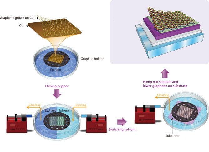
本所吳志毅教授研究團隊近期於ACS NANO 所發表的文章 (ACS Nano 2014, DOI: 10.1021/nn406170d),提出了一個全新轉印石墨烯的方法,獲得 C & EN (Chemical & Engineering News)雜誌專訪,專訪文章放於該雜誌的News of the Week,網址如下:
Cleaner Graphene Offers Better Device Performance
Web Date: February 10, 2014
Cleaner Graphene Offers Better Device Performance
News Channels: Materials SCENE, Nano SCENE
Keywords: graphene, chemical vapor deposition, copper, device fabrication
Graphene has a dirty little secret. When researchers build electronic devices with it, the standard process they use to move sheets of the delicate, single-atom-thick material into place can lead to contamination or damage that reduces device performance. But now, researchers in Taiwan have developed a simple and elegant way to transfer graphene
that keeps the material clean (ACS Nano 2014, DOI: 10.1021/nn406170d).
Scientists produce high-quality, large-area sheets of graphene by growing them on copper surfaces using a method called chemical vapor deposition.
These sheets often get used as electrodes in devices such as transistors, light-emitting diodes, and solar cells because of graphene’s excellent conductivity and transparency.
The first step in building these devices is to remove the graphene from the copper substrate. Unfortunately, this is where the contamination problems start, says Chih-I Wu, a professor of electrical engineering at National Taiwan University.
The most commonly used transfer method relies on placing a polymer-based material on the graphene to hold it in place while the metal below is etched away. The polymer, however, leaves behind an organic residue that contaminates the graphene. Some, but not all, of the residue can be removed with various solvents or heat treatments. Additionally, this cleaning stresses the material, resulting in a damaged sheet of graphene that doesn’t perform optimally, Wu says. Wu’s team reports a more direct, cleaner approach that starts with submerging a copper substrate and its attached graphene in a petri dish filled with a metal-etching solution. The solution frees the graphene, which then floats on the surface. The researchers then replace the etching solution with a mixture of isopropyl alcohol and water by using two syringes, one that slowly removes the etchant and another that injects the alcohol-water mixture.
Next, the researchers slip the device they’re building right below the floating graphene sheet. Using a syringe, the researchers remove the alcohol-water mixture completely, which lowers the graphene onto the device. Van der Waals forces between the graphene and the top of the device affix the two materials.
To test their new transfer method, the researchers made a series of devices, including a transparent organic solar cell.
The cell can absorb light on both sides by using graphene as electrodes on both the top and bottom of the device.
The researchers also made graphene-based transistors. Electrical charges could move 50% faster through the transistors than in those made with graphene transferred by polymer, demonstrating that the new method improved the quality of the transferred graphene.
Rodney S. Ruoff, a nanoengineer at the University of Texas, Austin, calls the approach “interesting and useful.” He suggests it could be used to make a type of extremely
low-power transistor with interesting quantum effects, called a BiSFET. Ideally, the graphene must be very clean to make such a device, Ruoff says.
The researchers plan to scale up their process. This demonstration used devices about an inch wide. To show the method is compatible with device manufacturing processes, the researchers hope to test the approach with 8-inch- or 12-inch-diameter silicon wafers.


