


June 2020 - August 2020
Publisher: Chairman Jian-Jang Huang
Editors: Professor Snow H. Tseng,
Ms. Hsiao-wen Lin | October 30, 2020
Editors: Professor Snow H. Tseng,
Ms. Hsiao-wen Lin | October 30, 2020

|
Congratulations to Prof. C. C. Yang for being granted with the status of “Nien Made - Ming Nien Chair Professor” by the National Taiwan University. Congratulations to Prof. Snow H. Tseng for being awarded “Presidential Excellent Teacher Award” by the Ministry of Education. |

Spatial Range of the Plasmonic Dicke Effect in an InGaN/GaN Multiple Quantum Well Structure
Professor C. C. Yang’s Lab.
Graduate Institute of Photonics and Optoelectronics, National Taiwan University
The plasmonic Dicke effect means a cooperative emission mechanism of multiple light emitters when they are simultaneously coupled with the same surface plasmon (SP) mode of a metal nanostructure to achieve a higher collective emission efficiency. Here, we compare the enhancements of emission efficiency among a series of SP-coupled InGaN/GaN quantum-well (QW) structures of different QW period numbers to show an emission behavior consistent with the plasmonic Dicke effect. The relative enhancement of overall emission efficiency increases with QW period number until it reaches a critical value, beyond which the enhancement starts to decrease. This critical QW period number corresponds to the effective depth range of the plasmonic Dicke effect in a multiple-QW system. It also represents an optimized QW structure for maximizing the SP coupling effect. Internal quantum efficiency (IQE) and time-resolved photoluminescence are measured for comparing the enhanced emission efficiencies of blue and green QW structures with different QW period numbers through SP coupling induced by surface Ag nanoparticles. Figure 1 below shows the structures of the 5 single-QW samples of different capping layer thicknesses and the 6 QW samples of different QW period numbers. Figure 2 shows the transmission spectra of those samples after Ag nanoparticles are placed on the top. The depressions correspond to the SP resonance feature. Figures 3 and 4 show the IQEs of those samples and their relative enhancements.

Fig. 1 (a): Structure of the 5 single-QW samples with different d. (b): Structure of the 6 QW samples with 1-6 QW period numbers.
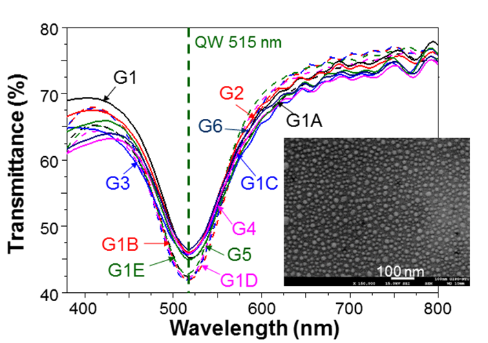
Fig. 2 Transmission spectra of the totally 11 samples shown in Fig. 1. The insert shows the SEM image of the Ag nanoparticles on the sample top to produce SP coupling.
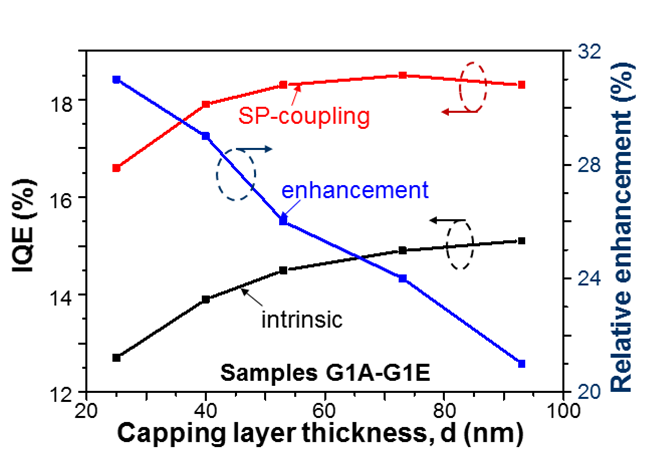
Fig. 3 Variations of the IQEs of the 5 single-QW samples and their relative enhancements.
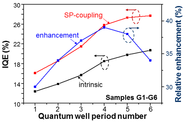
Fig. 4 Variations of the IQEs of the 6 QW samples of different QW numbers and their relative enhancements.
In0.53Ga0.47As/InP SAGCM avalanche photodetectors
Professor Hao-Hsiung Lin’s Lab.
Graduate Institute of Photonics and Optoelectronics, National Taiwan University
In this work, we report on the design and fabrication of In0.53Ga0.47As/InP avalanche photodetectors (APDs) with separated absorption, grading, charge sheet, and multiplication (SAGCM) structure. We used TCAD model to simulate 2D APD device structures with guard rings. The designed structures were realized on InP substrates by MOCVD growth and twice Zn diffusion processes. The depth of junction, thickness of the multiplication layer, and the depth of guard ring were controlled by the two diffusions. Fig. 1 shows the schematic diagram of the device structure and the fabricated APD devices. Fig. 2 shows the revise I-V of an APD in dark and under the illumination of a 1550 nm light source. Fitting results are also shown in the figure. Fig. 4 shows the measured external quantum efficiency of an APD with and without gain.
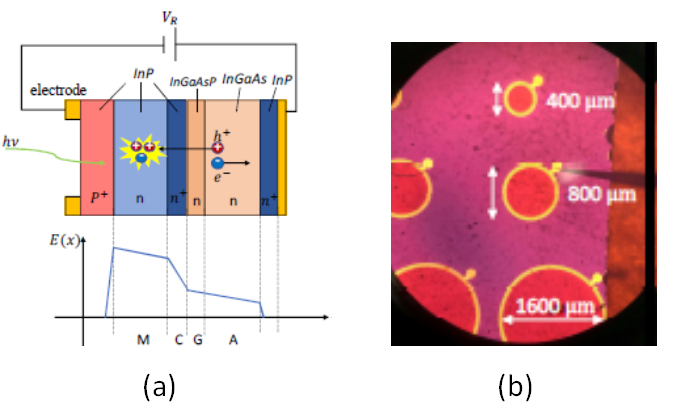
Fig. 1(a) Schematic diagrams showing the device structure and the electric field profile. (b) Microscope image showing APD devices.
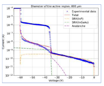
Fig. 2 Reverse dark and illuminated I-V curves of the APD devices. The 1550 nm light source induces the current jump at the punch through voltages. Fitting results from TCAD are also shown in the figure.
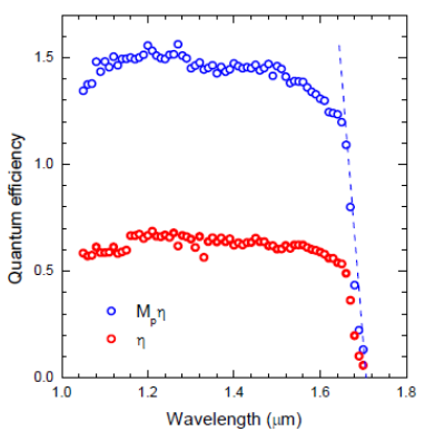
Fig. 3 External quantum efficiency of an APD device with gain (Mpη) and without gain (η).
Infrared broadband photodetector based on Schottky barrier of metal/Silicon
Professor Ching-Fuh Lin
Graduate Institute of Photonics and Optoelectronics, National Taiwan University
Generally speaking, silicon-based photodetectors are not suitable for the detection of 1550 nm, because the band gap of silicon is 1.12 eV, corresponding to the cut-off wavelength around 1100 nm. Therefore, the detection of infrared light is mainly based on III-V semiconductors or germanium, due to the low band gap. However, III-V materials and germanium are scarce and expensive relatively. In order to resolve above problems, we study the Schottky photodetector based on silicon. Since the silicon-based Schottky photodetector is associated with simple process, low cost and easy integration with electronic component, it has great potential for replacing III-V group and germanium.
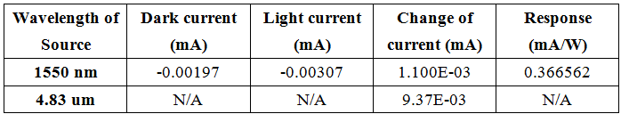
As an example, the Schottky photodetector of NiSi/n-Si/Au (Figure 1) has the response of about 0.37 mA/W for 1550 nm, as shown in Figure 2 and Table 1. This Schottky photodetector is applicable not only to 1550 nm, but also to MWIR of 4.83 um, also shown in Figure 2 and Table 1, the change of current for 4.83 um could be about 0.0094 mA.
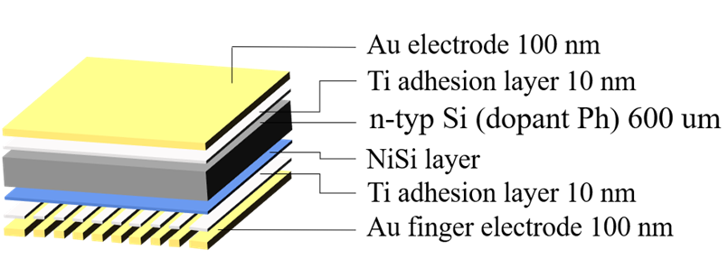
Fig. 1 The schematic diagram of Nisi/n-Si/Au Schottky photodetector.
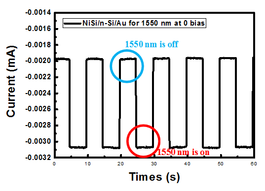
Fig. 2 Time–dependent photocurrents of NiSi/n-Si/Au for 1550 nm at 0 bias.
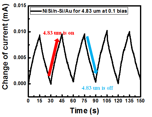
Fig. 3 Time–dependent photocurrents of NiSi/n-Si/Au for 4.83 um at +0.1 bias. (After fitting)
Table 1 The photovoltaic characteristics of NiSi/n-Si/Au for 1550 nm and 4.83 um.
Broadband Achromatic Metalenses at visible light
Professor Chieh-Hsiung Kuan
Graduate Institute of Photonics and Optoelectronics, National Taiwan University
Traditional bulky and heavy optical components usually use phase accumulation along optical path, spatial refractive-index distribution, or surface morphology to tailor the wavefront of electromagnetic waves. Novel metasurfaces have revolutionized the ways with which we design and engineer the wavefront shaping.With abrupt phase change at the surface, we can create the new wavefront with anomalous propagation by orderly arranging the nano-resonators on a metasurface that leads to functionalities that were impossible to realize in conventional devices are now made possible with such metasurfaces. Metalens is one application for the wavefront shaping of metasurfaces. In our E-beam lab, we have successfully developed a broadband achromatic metalens composed of GaN nano-rods that can eliminate chromatic aberration at visible light, showing a low-cost fabrication and high-efficiency platform, envisioning future optics.
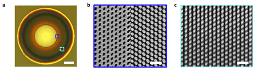
Fig. 1. (a) Optical image of the fabricated achromatic metalens. Scale bar: 10 μm. The dashed squares indicate the position of the zoomed-in SEM images shown in (b) and (c). Scale bars: 500 nm.
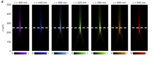
Fig. 2. Experimental light intensity profiles for the achromatic metalens. The white dashed line indicates the position of the focal plane.
Mobility Enhancement of Back-Channel-Etch Amorphous InGaZnO TFT with Double Layers
Professor Chee-Wee Liu
Graduate Institute of Photonics and Optoelectronics, National Taiwan University
The back-channel-etch amorphous InGaZnO (a-IGZO) double-layer thin-film transistor (DL-TFT) consists of an IGZO channel layer with no oxygen flow (NOF) and an IGZO barrier layer with oxygen flow (OF). The DL-TFT demonstrates the field-effect mobility of 19 cm2/ V-s, which is 1.6X of the NOF and the OF single-layer TFTs (SL-TFTs) at the overdrive voltage of 18V and the drain voltage of 0.1V. Several measurements are performed to obtain the band alignment between the NOF and the OF layer for further understandings of the mechanism of the improvement in the field-effect mobility. Tauc method, X-ray photoelectron spectroscopy (XPS), and Kelvin probe force microscopy (KPFM) measurements were used to extract the optical bandgaps, the Fermi level position, and the work function of the NOF and the OF, respectively. The conduction band difference of 0.28 eV between the NOF and the OF layer is obtained. The carriers in the DL-TFT are confined in the NOF layer by quantum confinement, where the OF layer serves as the barrier to reduce the Coulomb scattering between the channel electrons and oxide charge, and the surface roughness scattering from the IGZO/oxide interface. DL-TFT can achieve high mobility with manufacturing ability by the simple change of oxygen flow.
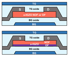 Fig. 1 Schematics of the cross-sectional diagrams (not scaled) of (a) SL-TFT and (b) DL-TFT. |
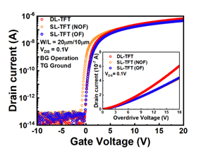 Fig. 2 Transfer characteristics of the SL-TFT with either NOF or OF channel, and the DL-TFT by bottom gate operation with top gate ground. The inset is the linear scale of drain current versus overdrive voltage. |
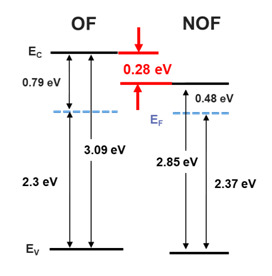 Fig. 3 The band alignment for NOF and OF a-IGZO. |
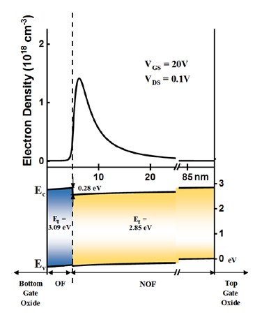 Fig. 4 Simulation of the electron density distribution and the band diagram of the DL-TFT. |
Copyright © Graduate Institute of Photonics and Optoelectronics, National Taiwan University
http://gipo.ntu.edu.tw/monthly
http://gipo.ntu.edu.tw/monthly