|
|
 |
| |
|
Publisher: Chairman Yuh-Renn Wu Editors: Professor Snow H. Tseng, Ms. Hsiao-wen
Lin December 30, 2024
|
| |
|
 |
|
Congratulations to Prof. Yuh-Renn Wu for the honor of achieving First Place in “University Faculty Softball Championship 2024.”
Congratulations to Prof. Yuh-Renn Wu and his PhD student Jun-Yu Huang for the honor of receiving the “IEEE RoC Branch PhD Thesis Award 2023.”
Congratulations to the following students for the honor of receiving the following awards:
| Student |
Award |
Advisor |
|
Sie-Beng Ting
(PhD)
Kuan-Chou Pu
(Master)
|
International Electron Devices & Materials Symposium 2024 (IEDMS 2024)
IEDMS Excellent Poster Award
Thesis Title: Effect of Device Architecture on the Charge Compensation and Ferroelectric Behavior in HfZrO2-Based Fe-TFTs with IGZO Channel
|
Prof. I-Chun Cheng
|
|
Lien-Chun Huang
(Master)
|
International Electron Devices & Materials Symposium 2024 (IEDMS 2024)
IEDMS Excellent Poster Award
Thesis Title: Anthracene-bidibenzofuran as host of blue organic light-emitting diode
|
Prof. Jiun-Haw Lee
|
|
Shao-An Chen
(Master)
|
International Electron Devices & Materials Symposium 2024 (IEDMS 2024)
IEDMS Outstanding Poster Award
Thesis Title: Green Thermally Activated Delayed Fluorescence Organic Light-Emitting Diode with Acridine Derivative emitter
|
Prof. Jiun-Haw Lee
|
|
Li-Hao Huang
(Master)
|
2024 Taiwan TFT Conference
Best Poster Award
Thesis Title: a-IGZO TFTs Made on Cellulose Nanopaper Substrates
|
Prof. I-Chun Cheng
|
|
|
|
|

|
|

|
|
| |
|
|
|
|
|
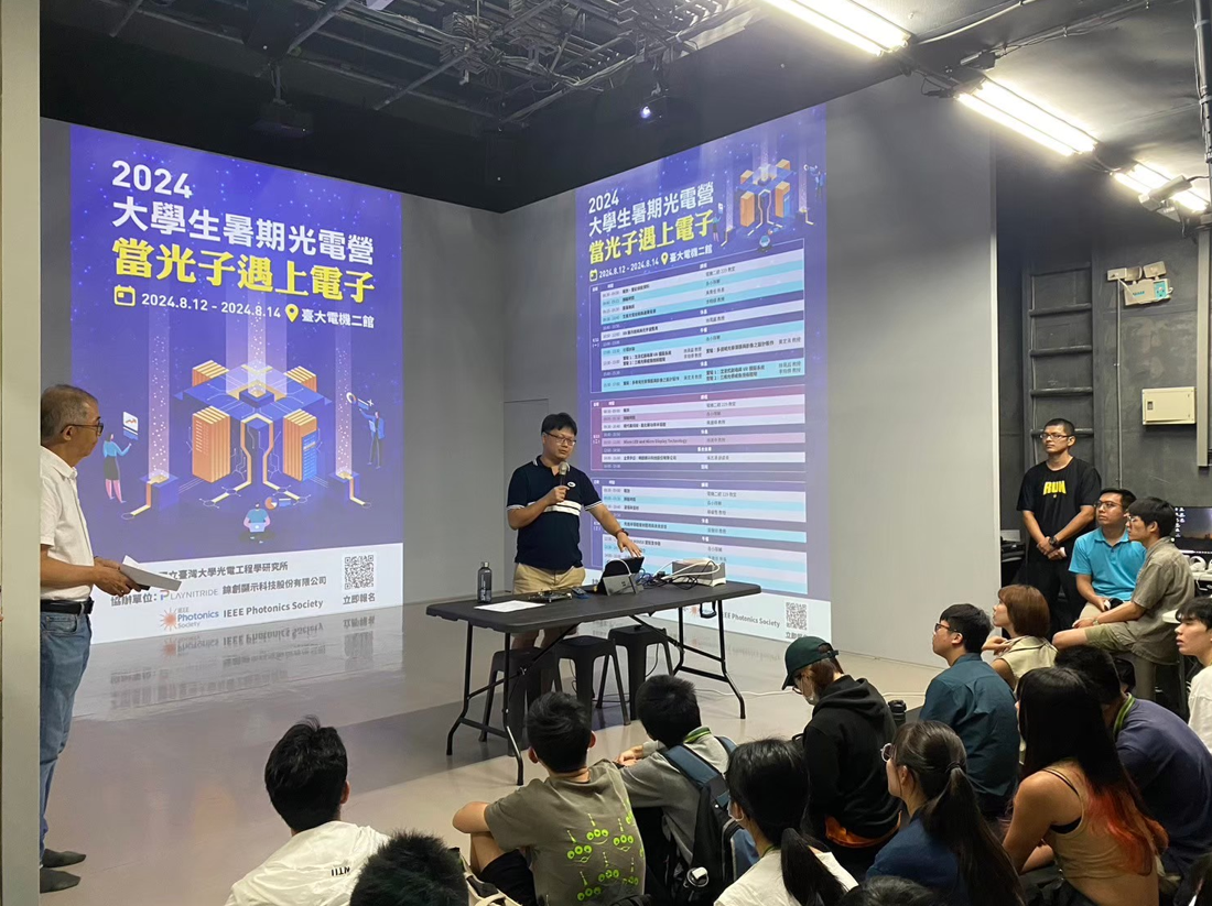
~ Optoelectronics Summer Camp 2024 ~
(August 12-14, 2024, EEII Building, National Taiwan University)
by Ching Chien
Every year during summer, NTU GIPO would hold a three-day summer camp to help undergraduates to better understand GIPO's research, with the hope that in the future they too may become a part of the photonics field. This year the summer camp was held from August 12-14 in the EEII
Building. The event began with Chairman Prof. Yuh-Renn Wu giving a brief overview of the current state and future developments in the photonics industry, introducing participants to areas of photonics that they might potentially take interest in. The first lecture by Prof. Hsiang-Chieh Lee explored biomedical photonics technology and its industrial development. Prof. Lee introduced many remarkable contributions of photonics to the field of medicine, including non-destructive 3D tomography for high-speed industrial inspection, optical coherence tomography and angiography for early diagnosis of cancer, research on compact or handheld optical imaging systems, non-invasive biomedical optical imaging technology, the development of intelligent image analysis algorithms, and the application of multi-tasking high performance imaging engines and edge computing.
Following, was Prof. Hoang-Yan Lin's seminar titled "XR Display Technology and Applications in the Metaverse," guiding the students to the realization that only through the continuation of inventions of more affordable ways to enable one to experience what would otherwise lie beyond one's natural abilities, can these methods become hallmarks of this era, when they become readily accessible to the public masses instead of being limited to few privileged individuals. Providing realistic travel experiences for people who are indoor-bound or simply don't have the time, opening up doors of opportunity to new worlds beyond their personal limitations, allowing them to gain information through introspection and continually expanding fields that resonate and spark their interests.
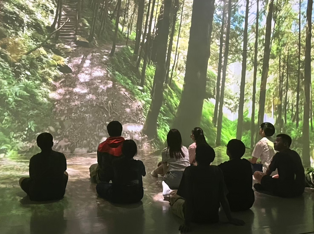
For the first afternoon, hands-on practical sessions were arranged for the students. Through Prof. Hoang-Yan Lin's "Immersive Theater and VR Simulation Systems," students experienced the amazing crossplay between the virtual and real world experience. The immersive theatrical performances took the audience into the story's setting, while the VR system enhanced the sensory stimulations, combining into a truly immersive experience. The most memorable part was the realism of the character interactions. Through the experiences brought about by environmental changes, this demonstrated how technology is reshaping our understanding of theater and entertainment. The sense of realism of the immersive theater and VR simulation systems created infinite possibilities for the future.
|
 |
|
Pig. 1. The VR simulation system experience at the experimental theatre |
Prof. Hsiang-Chieh Lee's "3D Optical Imaging Technology Experience" allowed participants to closely observe the structure of the skin, providing images with clarity beyond what a human eye was capable of unassisted. After explanations regarding the underlying principles, Prof. Lee guided participants to take turns using a handheld inspection device. The device's advantages include ease of operation, fast scanning speed, and instantaneous results. This technology, when used in skin health monitoring, can allow early detection of potential issues and provide more accurate diagnoses. Many participants were impressed by the precision and practicality of this technology, and were convinced of its extensive application prospects in the dermatology field and the beauty industry.
|
 |
|
Fig. 2. Prof. Hsiang-Chieh Lee giving a talk on the 3D imaging technology |
Additionally, in the course "Design and Fabrication of Multi-View Optical Films and Images," Prof. Ding-Wei Huang guided the participants on how to use optical films to create various imaging effects that changed with different viewing angles. This design is highly challenging in terms of not only the choice of materials, but also requires an in-depth understanding of optical principles. During the fabrication process, both the refraction and reflection of light were skillfully manipulated so that observers could see different effects from various viewing angles. This deepened the participants' understanding of optical applications and highlighted the significant potential of this technology in future display technology and security in anti-counterfeiting fields.
The core courses on the second day were "Micro LED and Micro Display Technology" and "Modern Cutting-Edge Technology—GaN Power Semiconductors" led by Prof. Chien-Chung Lin and Prof. Jian-Jang Huang. The professors introduced these critical technologies to the participants in an easy-to-understand manner, enabling participants to gain a deeper understanding of the future developments in photonics technology.
The Micro-LED technology, as a key technology in the future display field, boasts many advantages such as high brightness, low power consumption, long lifespan, and high resolution. During the class, Prof. Chien-Chung Lin provided a basic introduction to the technology, and highlighted that when compared to traditional OLED and LCD technologies, Micro-LED offered greater efficiency and color performance. These advantages are especially observable in the micro display field, making it highly suitable for applications in AR and VR, where high brightness, low latency, and high resolution are critical requirements.
Prof. Lin also discussed how the EUV (Extreme Ultraviolet) lithography system significantly enhanced LED efficiency in the Micro-LED manufacturing process and supported higher fabrication precision, which is crucial for further miniaturization of Micro-LED. Prof. Lin also introduced the potential of Gallium Arsenide (GaAs) and Indium Phosphide (InP) materials in 3D sensing and other high-end applications. In the future for the smart wearable devices, these materials, along with GaN, are expected to lead new directions in display technology.
In Prof. Jian-Jang Huang's course, he provided an easy-to-understand and thorough introduction to the latest developments and potential applications of GaN semiconductors and quantum dot technology. Prof. Huang emphasized that Gallium Nitride (GaN) semiconductors, due to their exceptional high-frequency and high-temperature performance, are being widely used in fields such as 5G, electric vehicles, and solar energy. Compared to traditional silicon-based semiconductors, GaN offered significant advantages in improving energy efficiency. In the field of quantum dot technology, Prof. Huang elaborated on its applications in display technology and medical imaging, particularly highlighting the breakthroughs in color performance and brightness, which provided a more realistic visual experience to displays.
Prof. Huang shared the progress of these technologies, and discussed the potential integration of GaN power semiconductors and quantum dot technology in the future, especially in innovative applications within energy management and display fields. Prof. Huang analyzed key technologies and trends, providing students with a clearer understanding on how these forward-looking technologies will transform aspects of our life, allowing the participants to gain a more concrete concept of future technological advancements and inspiring them to envision their own ideas for developments in the tech industry.
|
 |
 |
|
Fig. 3. Enthusiastic students engaging in discussion |
Fig. 4. Deputy Director Chih-Ling Wu gave an overview on the current trends in display and optical technology |
In the afternoon, continuing the theme of the day, the Chairman Prof. Yuh-Renn Wu took the participants on a trip to visit PlayNitride, located in Chunan, for a guided tour. Although the schedule was tight and demanding, enthusiasm remained throughout the journey. Upon arrival, Deputy Director Chih-Ling Wu gave an overview on the current trends in display and optical technology, followed by a brief introduction of PlayNitride's key developments. During the Q&A session, the participants engaged actively with the host, posing insightful and intriguing questions that showed strong interest in the display industry.
This year’s course design and the industry visit offered the participants a unique opportunity to delve deeper into advanced technologies like Micro LED and gain firsthand insight into the current state of optoelectronics industries. These experiences broadened their perspectives and fueled their anticipation for the future of the technological world. The knowledge and inspiration they gained served as valuable resources for their personal learning and exploration, shaping their academic and career aspirations in the field of optical and display technologies.
|
 |
|
Fig. 5. Group photo at PlayNitride |
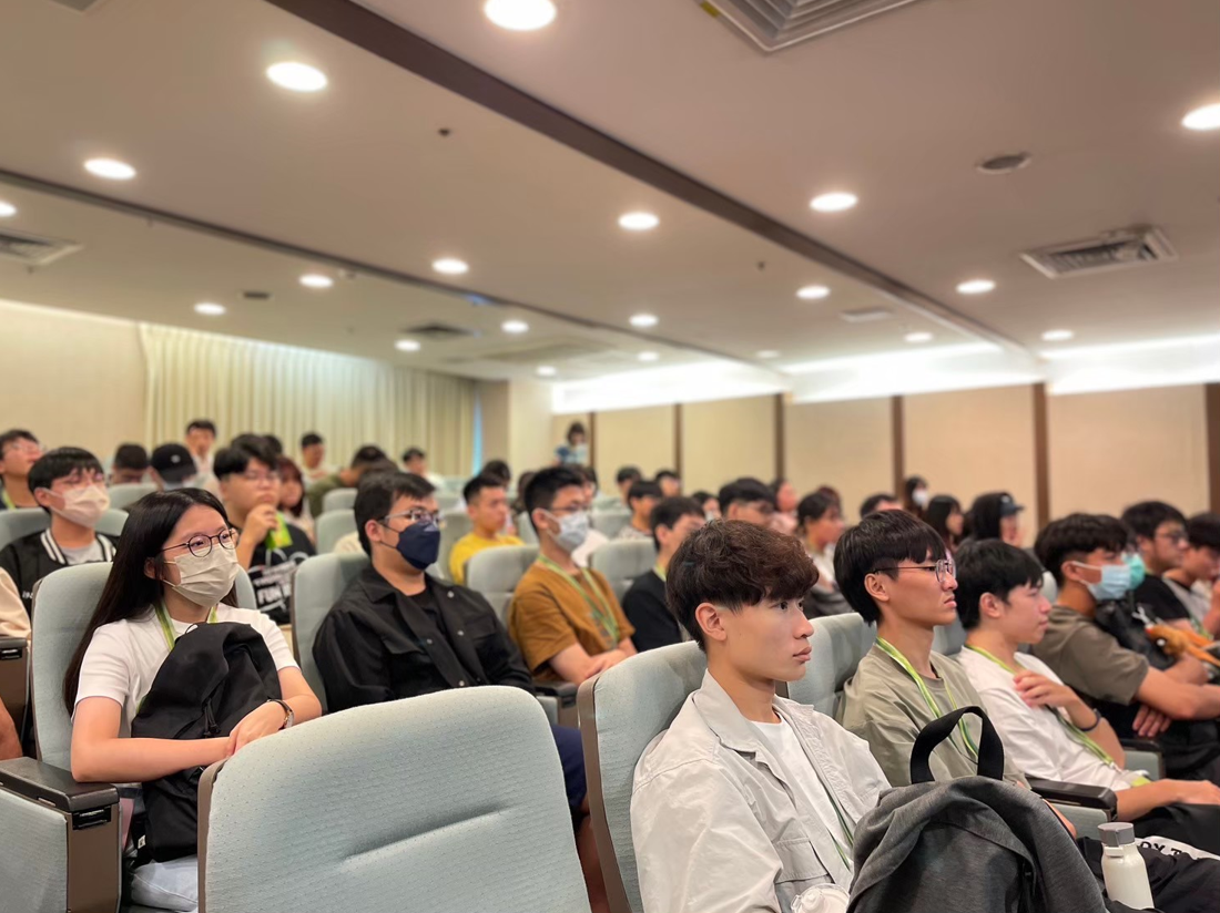
The third day was the lecture-based sessions. Prof. Jui-che Tsai's presentation on "Waveguides and Lasers" provided the participants with a comprehensive understanding of waveguide concepts, linking their physics knowledge to practical waveguide technology. This session not only addressed the potential knowledge gaps that the participants might have, but also solidified their grasp on the waveguide fundamentals and its applications in laser technology. These knowledge will be of great significance for the students as they pursue future research and career opportunities in related fields.
Prof. Chao-Hsin Wu's lecture on "Advanced Semiconductor Laser Applications and Future Prospects" provided participants with a comprehensive insight into the future of the semiconductor industry. As modern electronic devices continue to reduce in size, the demand for smaller and smaller semiconductor components has only increased, continuously driving the requirements for efficiency, speed, and precision in the manufacturing processes. In this context, the laser processing technology was known for its exceptional precision and stability, and has found extensive application in the semiconductor manufacturing field. This technology has not only enhanced the manufacturing process efficiency, but also fostered continual progress and innovation in semiconductor technology. By learning these advanced knowledge, students gained better understandings of the future technological trends and established a stronger foundation for further research and practical application.
|
 |
|
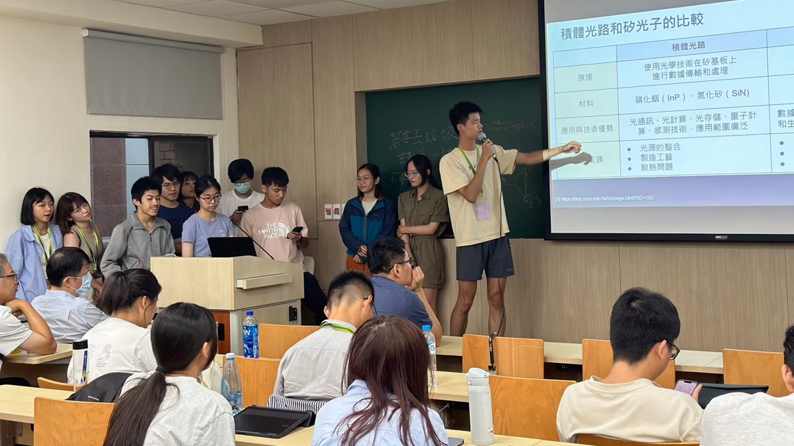
Fig. 6. The students’ presentation of their thoughts and findings |
|
 |
|
Fig. 7. Chairman Prof. Yuh-Renn Wu and the award winning groups |
During the summer camp, the participants were engaged in various interactive activities that allowed them to apply the knowledge they gained and engage in in-depth discussions with the experts in the industry. These experiences not only enhanced their practical skills but also showed the importance of teamwork. On the final day, the students visited various labs to explore different research themes and their applications, which broadened their perspectives and deepened their interest in the field of optoelectronics. Afterwards, each team gave a presentation, which was evaluated by professors, and the top three teams were awarded. The summer camp concluded with a group photo of all participants, marking a successful and enriching end to the optoelectronics camp.
|
 |
|
Fig. 8. Successful conclusion of the summer camp |
|
|
|
|
|
|
|
|
|
| |
|
|
|
|
|
Noise Reduction Through Square Aperture Array in Integral Imaging-based 3D Light-Field Display
Professor Hoang-Yan Lin
Graduate Institute of Photonics and Optoelectronics, National Taiwan University
The integral-imaging based 3D light field display can restore its light-field information, reconstruct different images in different depth planes, and realize the floating projection effect. In the metaverse, AR/VR wearable devices, HUD for smart cockpits, medical care, entertainment, art performance and other scenarios, naked-eye 3D display is one of the most crucial requirements for the coming future.
We have created 3D floating images with an integral imaging-based 3D light field display. However, noise is an annoying problem after restoring information in 3D light field displays. In this study, we proposed a square aperture array to be added to the original light field display to solve the noise problem and find out that an aperture array can effectively decrease the noise. Also, the light intensity will be decreased a lot for the circle aperture array case but will not be decreased for our square aperture array design. Finally, we created naked-eye 3D images with very little noise and also without light intensity sacrifice.
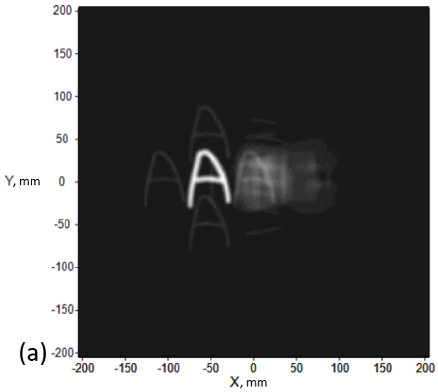
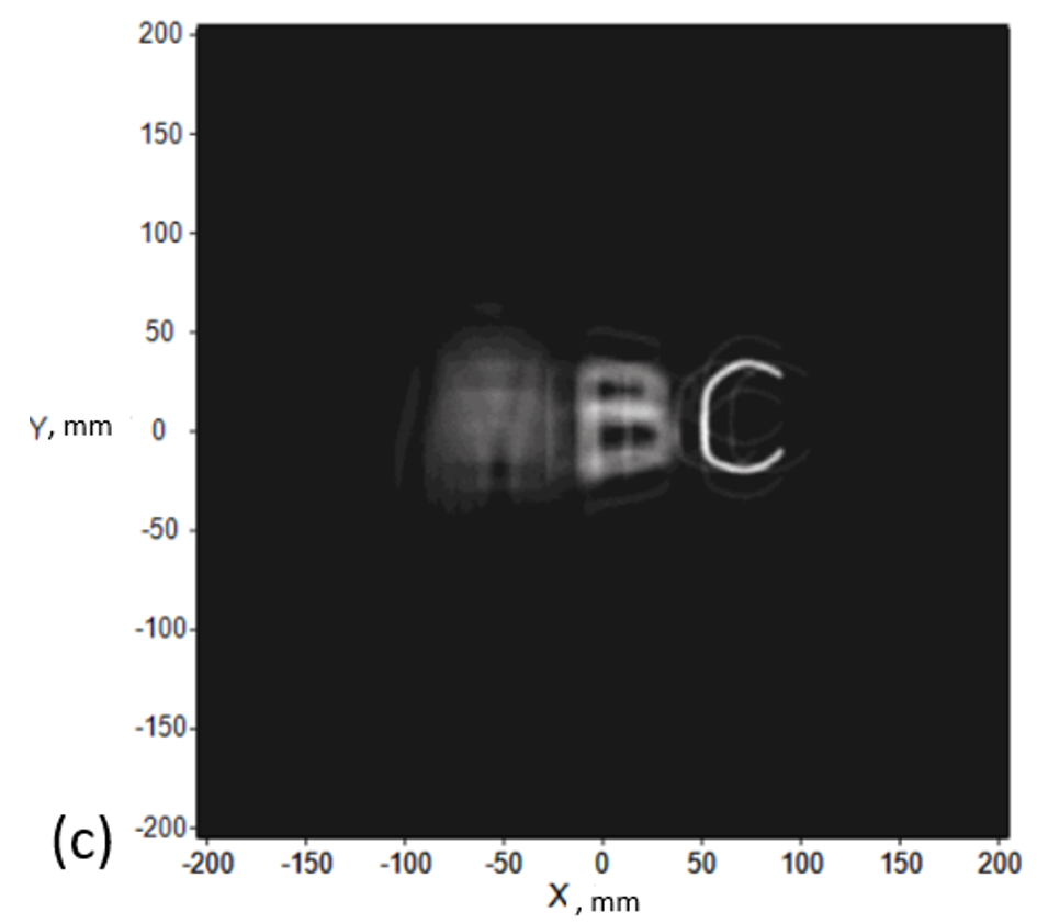
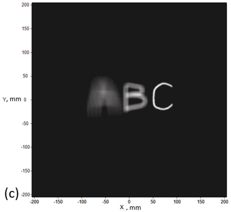
Firstly, we show a light-emitting angle = 90 degrees for the sample, we will create a picture at different depths (z) as shown in Fig. 1. Looking closely at Figs. 1 (a)(b)(c), we can find out that there are 4 dim letters A around the bright letter A and the same situation in letters B and C. We regard those dim letters as noise and it is produced by a light ray that does not obey the principle of CGEI.
|
|
|
|
|
Fig. 1. Images in different depths (z) (a) A at z = 200mm (b) B at z = 105.37 mm (c) C at z = 48 mm.
|
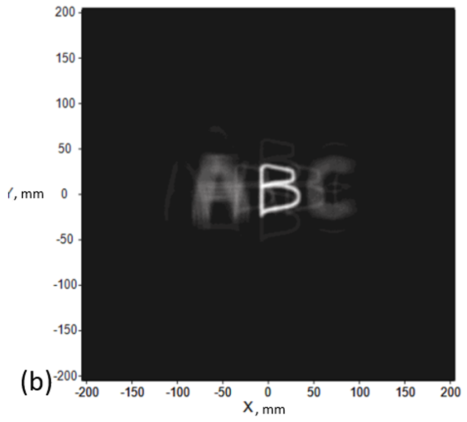
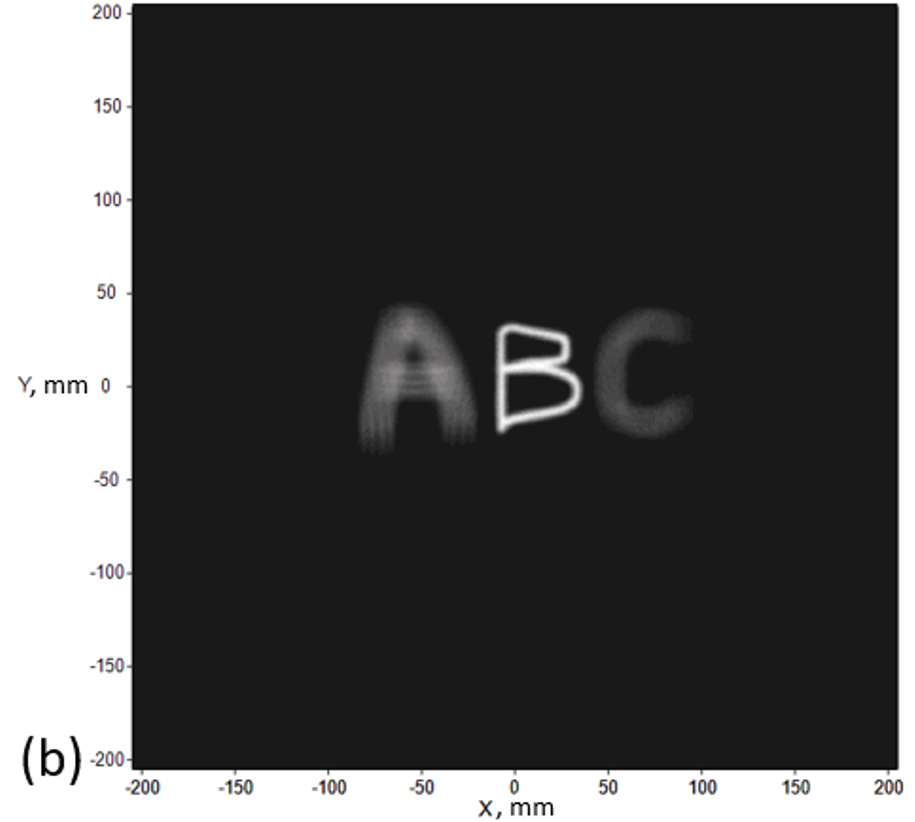
After knowing the best position of the aperture array, we have shown the restored image in different depths (z) in Fig. 2 when aperture array X=7 mm. We set parameter X for the distance between the aperture array and the display panel. We can discover that there isn’t any dim letter next to the bright letter, which means that we successfully eliminate the noise!
|

|
|
|
|
Fig. 2 Image in different depths with aperture array (a) A at z = 200mm (b) B at z = 105.37 mm (c) C at z = 48 mm.
|
Reference:
Chia-Yuan Chang and Hoang-Yan Lin, Noise Reduction Through Square Aperture Array in Integral Imaging-based 3D Light-Field Display, SID Display Week 2023.
Photonic Mixing Sub-THz Carrier for Wireless Data Link with Single-Chip Dual-Wavelength DFBLD
Professor Gong-Ru Lin
Graduate Institute of Photonics and Optoelectronics, National Taiwan University
Sub-THz wireless communication technology has emerged as a promising candidate to extend the carrier frequency toward previously unexplored bands to enable the ultra-wide-band short-range data link beyond 6G. The optical heterodyned generation of millimeter-wave wireless carriers via discrete laser sources is intriguing in view of the currently available technologies for carrier synthesis because of its flexibility on frequency tunability. However, finite modal linewidth and residual wavelength drift are two main concerns that raise the noise background to degrade the signal-to-noise ratio of the data encoded onto the heterodyned carrier. Maintaining the difference and stability of wavelength and phase between two independent lasers usually relies on additional controlling and feedback schemes such as a phase-locked loop. This inevitably induces systematic complexity and alternative solution needs to be considered for simplification. In this work, a dual-mode distributed feedback laser diode (DFBLD) is demonstrated as a monolithic wireless sub-THz carrier synthesizer with absolute wavelength (frequency) differentiation and phase synchronization between two lasing longitudinal modes. By directly encoding the DFBLD with QAM-OFDM data format, the wireless data link can be performed via such a compact and simplified sub-THz wireless transmitter.
|
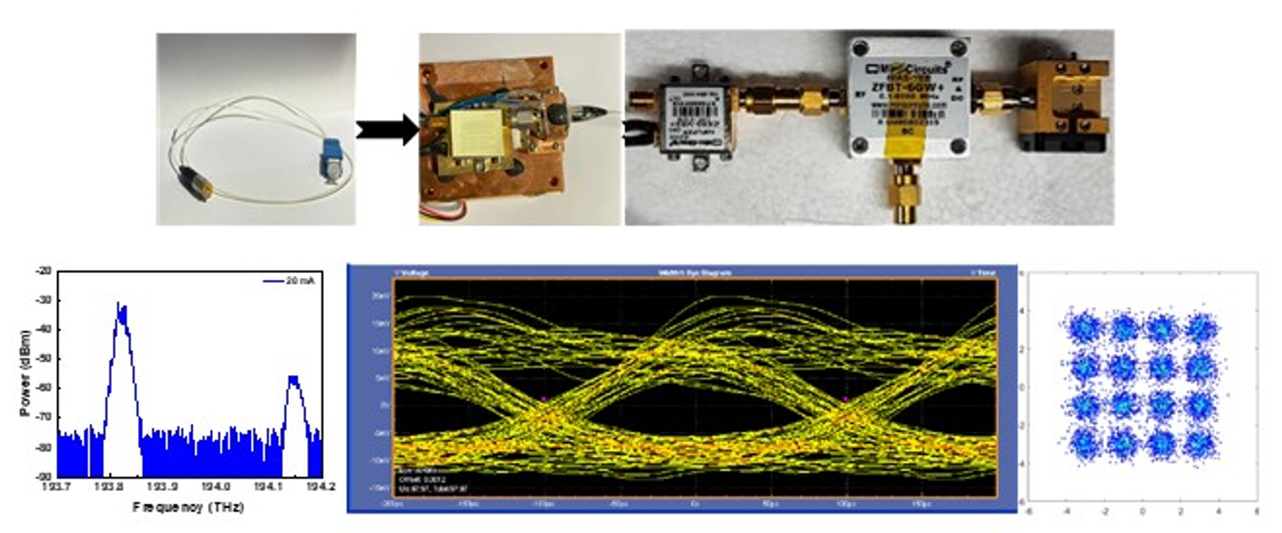
|
The dual-mode-lasing DFBLD is designed by slightly tilting the DFB mirror structure by an angle Φ to the surface normal of the output end-face at one side of the resonant cavity, which enables the concurrent lasing of both longitudinal modes inside the DFBLD cavity. Such a design combined with a short cavity results in a mode spacing of 2-3 nm to cause a frequency difference tunable from 320 to 330 GHz. The dual-mode-lasing DFBLD exhibits two distinct longitudinal modes centered at 1545-1546 nm and 1547-1548 nm, respectively. The back-to-back sub-THz wireless link is demonstrated by transmitting the NRZ-OOK data stream at 5 GBaud, revealing the quality factor and bit-error ratio of nearly 4 and 5e-5, respectively. By amplifying the 16-QAM DMT data amplitude, the received constellation plot of the down-converted baseband DMT data shows a blurred spot with an increased EVM. The signal-to-noise ratio remains above 15 dB over 95% of the encoding bandwidth, providing a BER of 2.3x10⁻³ of the broadened 16-QAM formats at allowable data rates of 12 Gbit/s. The fully integrated dual-mode-lasing DFBLD chip can serve as a novel compact sub-THz transmitter as compared to those using individual laser sources and external data modulators.
〔This work is the result of a collaboration with Professor Yu-Hsiang Cheng from the Department of Electrical Engineering at National Taiwan University.〕
Reference:
1. C.-Y. Lin, Y.-C. Chi, C.-T. Tsai, H.-Y. Wang, and G.-R. Lin, “39-GHz millimeter-wave carrier generation in dual-mode colorless laser diode for OFDM-MMWoF transmission,” IEEE J. Sel. Top. Quantum Electron., vol. 21, pp. 609-618, Nov.-Dec. 2015
2. C.-T. Tsai, C.-H. Lin, C.-T. Lin, Y.-C. Chi, and G.-R. Lin, “60-GHz millimeter-wave over fiber with directly modulated dual-mode laser diode,” Sci. Rep. vol. 6, no. 27919, Jun. 2016.
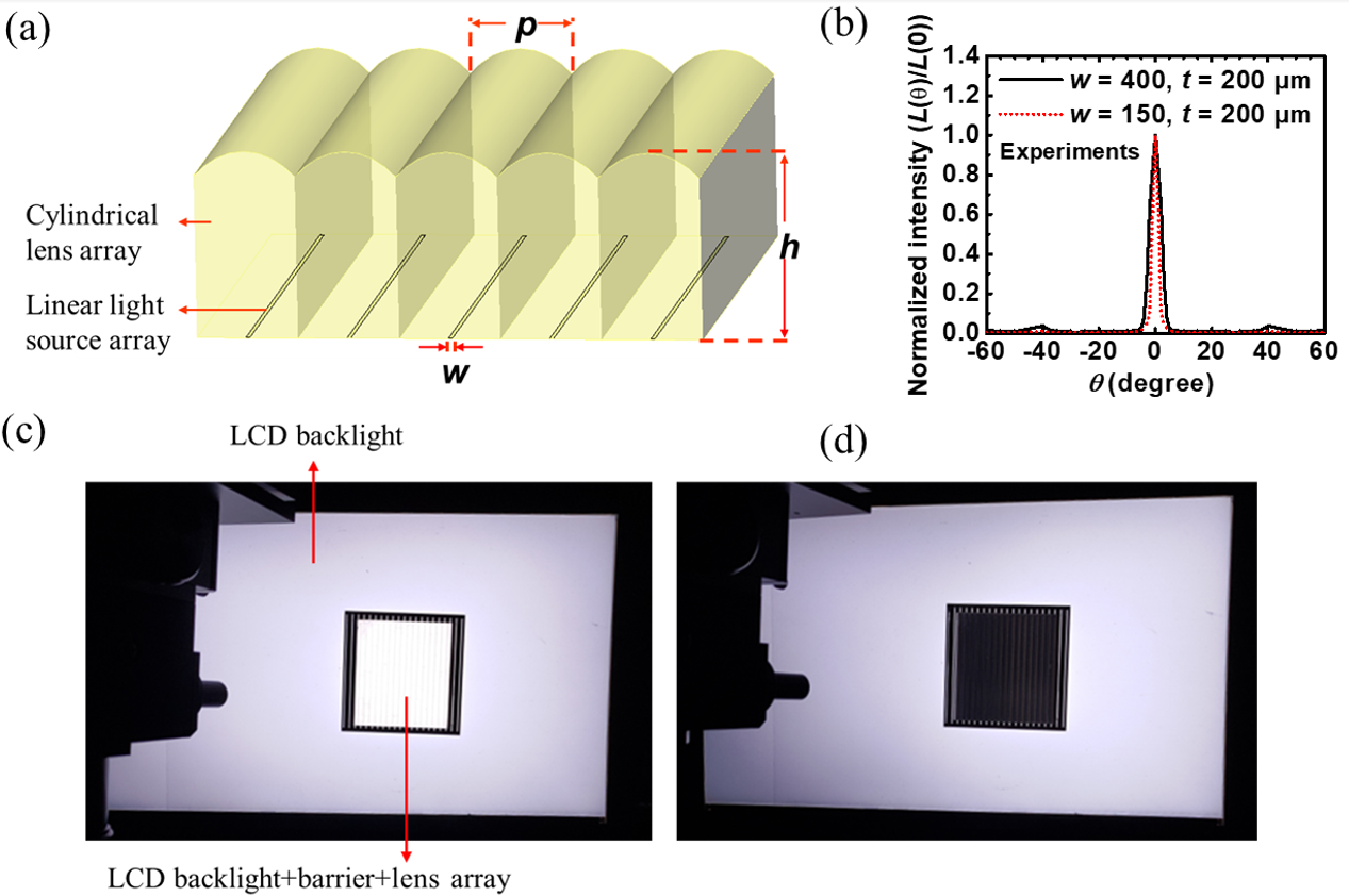
Simple Architecture for Highly Collimated Backlight
Professor Chung-Chih Wu
Graduate Institute of Photonics and Optoelectronics, National Taiwan University
Highly collimated and directional backlights are essential for realizing advanced display technologies such as autostereoscopic 3D displays. Previously reported collimated backlights, either edge-lit or direct-lit, in general still suffer unsatisfactory form factors, directivity, uniformity, or crosstalk etc. In our study, we devise a simple stacking architecture for the highly collimated and uniform backlights, by combining linear light source arrays and carefully designed cylindrical lens arrays. Experiments were conducted to validate the design and simulation, using the conventional edge-lit backlight or the direct-lit mini-LED (mLED) arrays as light sources, the barrier sheets, and cylindrical lens arrays fabricated by molding. Highly collimated backlights with small angular divergence of ±1.45°~±2.61°, decent uniformity of 93-96%, and minimal larger-angle sidelobes in emission patterns were achieved with controlled divergence of the light source and optimization of lens designs. Such an architecture provides a convenient way to convert available backlight sources into a highly collimated backlight, and the use of optically reflective barrier also helps recycle light energy and enhance the luminance, providing a facile approach for display technologies requiring highly collimated backlights.
|
|
|
Fig. 1. (a) The schematic architecture of the highly collimated backlight. (b) Measured far-field emission patterns of the collimated backlight. (c)-(d) Light-up photos of the conventional LCD BLU stacked with the barrier and the cylindrical lens array (center area), taken along (c) the normal direction (0°) and (d) the 5° tilting angle.
|
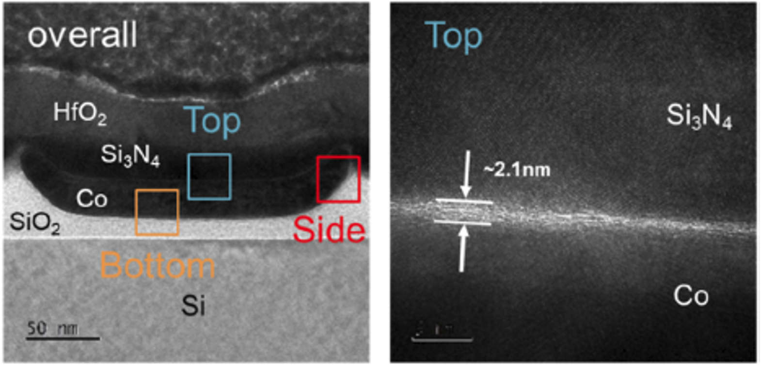
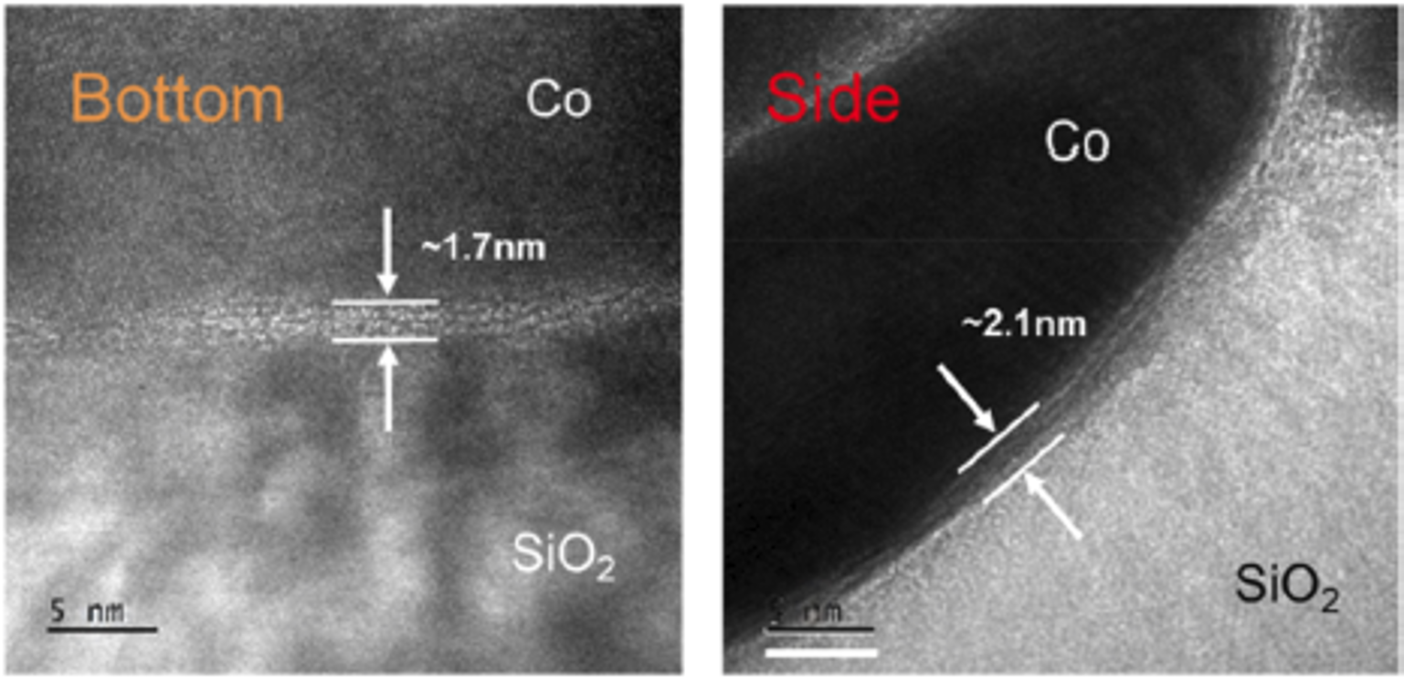
Graphene-All-Around Cobalt Interconnect with a Back-End-of-Line Compatible Process
Professor Chih-I Wu
Graduate Institute of Photonics and Optoelectronics, National Taiwan University
The continuous scaling of semiconductor devices has enabled the integration of increasing numbers of transistors on a single chip, leading to higher performance and functionality.1 Copper (Cu) interconnects have been widely used in the semiconductor industry due to their excellent electrical conductivity and low resistivity. However, as the size of the devices continues to shrink, the interconnects that connect the transistors and other components face significant challenges. To overcome these challenges Co interconnects are considered to be promising candidates for future interconnects in advanced technology nodes.
|

|
|
Fig. 1. Schematic of the HW-CVD process setup. The inset shows an GAA structure schematic. Statistical distribution of the Co EM lifetime for Si3N4/Co (black) and Si3N4/GAA/Co (red).
|
The graphene-all-around (GAA) structure has been verified to grow directly at 380 °C using hot-wire chemical vapor deposition, within the thermal budget of the back end of the line (BEOL), as shown in Fig. 1. The cobalt (Co) interconnects with the GAA structure have demonstrated a 10.8% increase in current density, a 27% reduction in resistance, and a 36 times longer electromigration lifetime. X-ray photoelectron spectroscopy and density functional theory calculations have revealed the presence of bonding between carbon and Co, which makes the Co atom more stable to resist external forces. The Co interconnect within the GAA structure (Fig. 2) exhibits enhanced electrical properties and reliability, which indicates compatibility applications as next-generation interconnect materials in CMOS BEOL.
|
|
|
|
Fig. 2. HRTEM images of graphene all around the structure on the top, bottom, and side in a single damascene Co interconnect.
|
Publish:
Kuo, C. Y., Zhu, J. H., Chiu, Y. P., Ni, I. C., Chen, M. H., Wu, Y. R., & Wu, C. I. (2024). Graphene-All-Around Cobalt Interconnect with a Back-End-of-Line Compatible Process. Nano Letters, 24(6), 2102-2109.
|
|
|
|
|
|
|
|
|
|
|
 |
|
 |
|