|
3D Staggered PSTD Modeling of Structural Coloration in Morpho Butterfly Wings
Professor Snow H. Tseng's Laboratory
Graduate Institute of Photonics and Optoelectronics, National Taiwan University
Simulation analysis of the vivid structural colors of Morpho butterfly wings, utilizing three-dimensional staggered pseudospectral time-domain (PSTD) techniques. By overcoming the computational limitations often associated with traditional finite-difference time-domain (FDTD) methods, the PSTD model reduces the grid resolution required for accurate 3D simulations.
By leveraging staggered PSTD, we achieve high-fidelity results while mitigating the Gibbs phenomenon, providing more precise visualizations and insights into how light interacts with these microstructures. Reflectance and luminance analyses are employed to investigate the optical mechanisms. The findings are translated into RGB representations for intuitive visualization, offering insights into the structural color phenomena observed in Morpho wings.
|
|
|
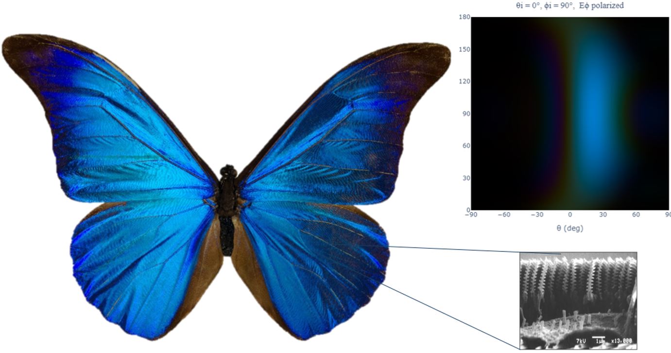
Fig. 1. (Left) A Morpho butterfly showing its characteristic blue structural coloration [1]. (Right, top) Simulated RGB representation of structural coloration according to observation angles in spherical coordinates. The horizontal axis represents the θ angle, and the vertical axis represents the Φ angle. (Right, bottom) Scanning electron microscope (SEM) image of the microstructures on the wing [2], demonstrating the ridge and lamellae structure responsible for the optical effects.
|
Reference:
[1] https://commons.wikimedia.org/wiki/File:Morpho_rhetenor_rhetenor_MHNT_dos.jpg.
[2] Kinoshita, S. and S. Yoshioka (2005). "Structural colors in nature: the role of regularity and irregularity in the structure." ChemPhysChem 6(8): 1442-1459.
Augmented Reality Display by Metalenses and Micro-LEDs
Professor Guo-Dung Su
Graduate Institute of Photonics and Optoelectronics, National Taiwan University
Augmented reality (AR), a technology that superimposes virtual information onto a user’s direct view of real-world scenes, is considered one of the next-generation display technologies and has been attracting considerable attention. Here, we present a flat optic AR system that synergistically integrates a polarization-independent metalens with micro lightemitting diodes (LEDs). A key component is a meticulously designed metalens with a numerical aperture of 0.25, providing a simulated focusing efficiency of approximately 76.5% at a wavelength of 532 nm. Furthermore, the laser measurement system substantiates that the fabricated metalens achieves a focusing efficiency of 70.8%. By exploiting the reversibility of light characteristics, the metalens transforms the divergent light from green micro-LEDs into a collimated beam that passes through the pupil and images on the retina. Monochromatic pixels with a size of 5×5 μm2 and a pitch of 10 μm can be distinctly resolved with a power efficiency of 50%. This work illustrates the feasibility of integrating the metalens with microdisplays, realizing a high-efficiency AR device without the need for additional optical components and showcasing great potential for the development of near-eye display applications. The experimental demonstration of the AR device is shown in the figure below.
|
|
|
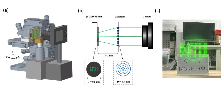
Figure (a) Experimental setup for the AR system. (b) The detailed cross-sectional schematic illustration of the components in this system. (c) Augmented image captured by the camera.
|
Blue triplet-triplet fusion organic light-emitting diode with bi-layer emitting layer
Professor Jiun-Haw Lee
Graduate Institute of Photonics and Optoelectronics, National Taiwan University
A blue organic light-emitting diode (OLED) based on triplet-triplet fusion (TTF) was demonstrated consisting of bi-layer emitting layer (EML) structure, which were 1-(2,5-dimethyl-4-(1-pyrenyl)phenyl)pyrene (DMPPP) and carbazole-substituted anthracene (CbzAn) which acted as triplet tank layer (TTL) and triplet-triplet fusion (TTF) layer, respectively. 5% of 7,7,13,13-tetramethyl-N5,N5,N11,N11-tetraphenyl-7,13-dihydrobenzo-[g]indeno[1,2-b]fluorene-5,11-diamine (DPaNIF) was incorporated inside TTL and TTF layer as dopants. Carriers recombined at the TTL which formed 25% singlets and 75% triplets. Singlet emission happened in TTL, while triplets transferred the energy to TTF layer undergoing upconversion process followed by light emission. External quantum efficiency of this blue OLED achieved remarkably 11.12%.
Reference:
Kai-Hong Hsieh et al., Adv. Photonics Res. 2024, 2300344.
Surface Acoustic Wave Actuated Plasmonic Signal Amplification in a Plasmonic Waveguide
Professor Jian-Jang Huang's Laboratory
Graduate Institute of Photonics and Optoelectronics, National Taiwan University
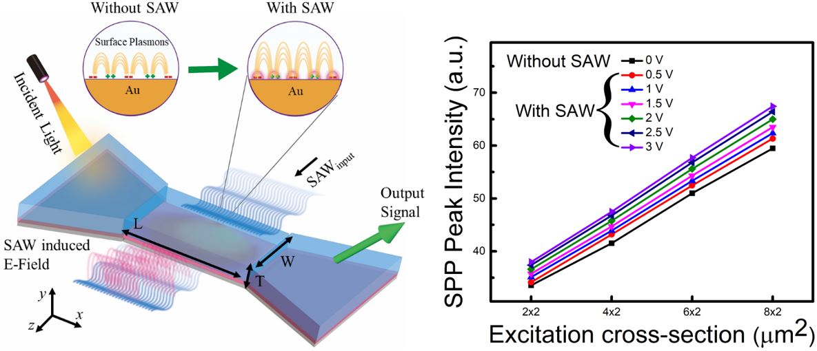
Enhancement of nanoscale confinement in the subwavelength waveguide is a concern for advancing future photonic interconnects. Rigorous innovation of plasmonic waveguide-based structure is crucial in designing a reliable on-chip optical waveguide beyond the diffraction limit. Despite several structural modifications and architectural improvements, the plasmonic waveguide technology is far from reaching its maximum potential for mass-scale applications due to persistence issues such as insufficient confined energy and short propagation length. This work proposes a new method to amplify the propagating plasmons through an external on-chip surface acoustic signal. The gold-silicon dioxide (Au-SiO2) interface, over Lithium Niobate (LN) substrate, is used to excite propagating surface plasmons. The voltage-varying surface acoustic wave (SAW) can tune the plasmonic confinement to a desired signal energy level, enhancing and modulating the plasmonic intensity. From our experimental results, we can increase the plasmonic intensity gain of 1.08 dB by providing an external excitation in the form of SAW at a peak-to-peak potential swing of 3 V, utilizing a single chip.
|
|
|