|
September 2023 - November 2023
|
| |
|
|
|
 |
|
 |
| |
|
Publisher: Chairman Yuh-Renn Wu Editors: Professor Snow H. Tseng, Ms. Hsiao-wen
Lin February 29, 2024
|
| |
|
 |
|
Congratulations to the following research groups for the honor of being awarded "Future Technology Award 2023."
| Research Title |
Project Director and Co-Directors |
|
Semiconductor laser quantum encryption key distribution and communication transceiver
|
Gong-Ru Lin, Yuh-Renn Wu, Ding-Wei Huang, Guo-Dung Su, Chao-Hsin Wu, Chao-Yang Wu
|
|
Extreme high index gate stacks integration on high layer number stacked transistor; Stacked nano layer field effect transistor; Indium gallium zinc oxide surround gate contact type nano-layer field effect transistor
|
Chee-Wee Liu, Min-Chang Chen
|
|
Extreme low light imaging technology: Capturing unseeable lights
|
Shun-Wei Liu, Jiun-Haw Lee, Yu-Ching Huang
|
Congratulations to Prof. Chih-I Wu for the honor of being awarded "30th TECO Award (Optoelectronics/Information/Communication)."
Congratulations to Prof. Yuh-Renn Wu for the honor of being awarded "Taiwan-France Technology Award 2023" in collaboration with Marcel Filoche of CNRS.
Congratulations to Prof. Chao-Hsin Wu for the honor of being awarded "2024 Optica Fellow."
Congratulations to the following students for being awarded:
| Student |
Award |
Advisor |
|
Yuan-Ming Liu
(PhD Student)
Yu-Chiao Chen
(Master Student)
Yu-Cheng Fan
(Master Student)
|
MRS-T Huali-Li New Materials Gold Award 2023
|
Prof. Chee-Wee Liu
|
|
Shaobo Yang
(PhD Student)
|
The 14th International Conference on Nitride Semiconductors (ICNS-14)
Best Student Award
|
Prof. C. C. (Chih-Chung) Yang
|
|
Hao Lee
(Master Student)
|
The 14th International Conference on Nitride Semiconductors (ICNS-14)
Best Student Award
|
Prof. Yuh-Renn Wu
|
|
Tai-Ang Wang
(PhD Student)
|
TSBME Biomedical Engineering Conference Distinguished Poster Award 2023
|
Prof. Hsiang-Chieh Lee
|
|
Yin-Shen Cheng
(PhD Student)
|
TSBME Biomedical Engineering Conference Poster Award 2023
|
Prof. Hsiang-Chieh Lee
|
Congratulations to Prof. Yuh-Renn Wu,
Ms. Li-Chi Yao, and
Ms. Ching Chien for representing GIPO in NTU Faculty Sports Competition 2023, and achieving 3rd place in the 1200M Triethalon.
|
|
|
|

|
|

|
|
| |
|
|
|
|
|
September “GIPO Colloquium” Highlights
|
|
Time:
|
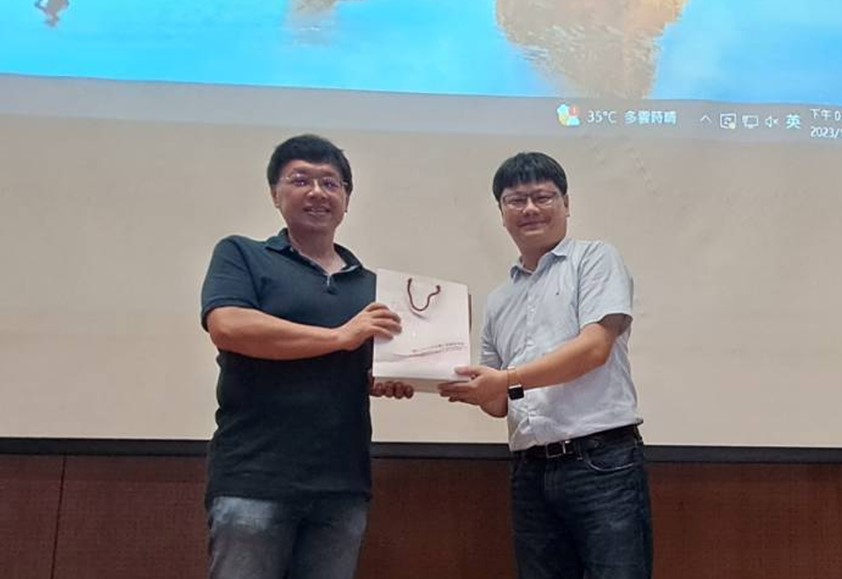
3:00 pm, September 8 (Fri.), 2023
|
|
Speaker:
|
Prof. Sabina Merlo (Department of Electrical, Computer and Biomedical Engineering, University of Pavia)
|
|
Topic:
|
Electromechanical characterization of M(O)EMS by spot optical interferometric techniques
|
|
|
|
|
Prof. Sabina Merlo (Right) and Prof. Sheng-Lung Huang (Left)
|
|
|
Time:
|
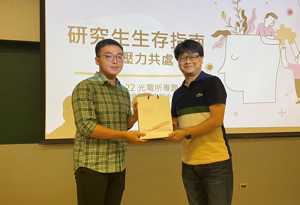
2:20 pm, September 22 (Fri.), 2023
|
|
Speaker:
|
Mr. Tzu-Ming Lin (Center for Student Well-Being, NTU)
|
|
Topic:
|
Survival Guide to Graduate Institute - Living with Stress
|
|
|
|
|
Mr.
Tzu-Ming Lin (Left) and Prof. Hsiang-Chieh Lee (Right)
|
|
|
October “GIPO Colloquium” Highlights
|
|
Time:
|
2:20 pm, October 6 (Fri.), 2023
|
|
Speaker:
|
Prof. Chih-Kuang Yeh (Department of Biomedical Engineering and Environmental Sciences, National Tsing Hua University)
|
|
Topic:
|
Acoustic vortex for confining light fluence
|
|
|
|
|
Prof. Chih-Kuang Yeh (Left) and Prof. Hsiang-Chieh Lee (Right)
|
|
|
Time:
|
2:20 pm, October 13 (Fri.), 2023
|
|
Speaker:
|
Prof. Lung-Chien Chen (Department of Electro-Optical Engineering, National Taipei University of Technology)
|
|
Topic:
|
Progress of all-inorganic perovskite quantum dot light-emitting diodes
|
|
|
|
|
Prof. Lung-Chien Chen (Left) and Prof. Hsiang-Chieh Lee (Right)
|
|
|
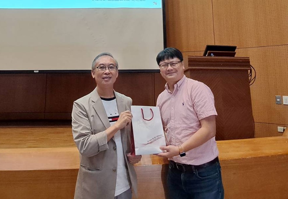
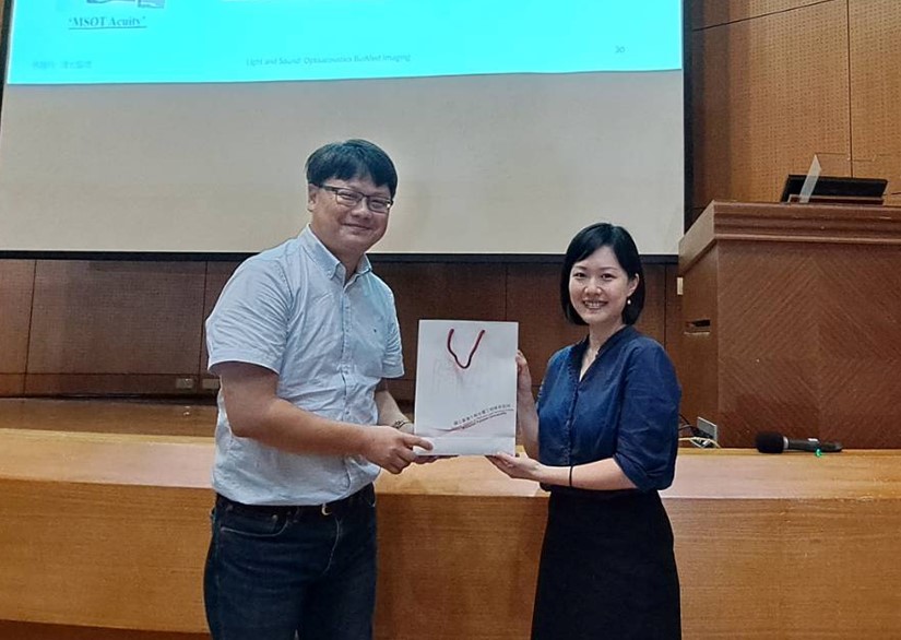
Time:
|
2:20 pm, October 20 (Fri.), 2023
|
|
Speaker:
|
Prof. Hsiao-Chun Lin (Department of Biomedical Engineering and Environmental Sciences, National Tsing Hua University)
|
|
Topic:
|
Light and Sound: Biomedical Optoacoustic Imaging
|
|
|
|
|
Prof. Hsiao-Chun Lin (Right) and Prof. Hsiang-Chieh Lee (Left)
|
|
|
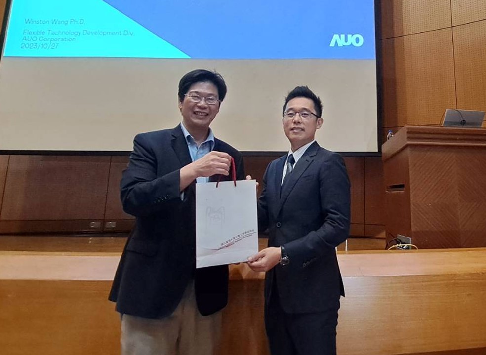
Time:
|
2:20 pm, October 27 (Fri.), 2023
|
|
Speaker:
|
Director Wan-Tsang Wang (Advanced Technology Center, AUO)
|
|
Topic:
|
Flexible Technology Evolution: from Rigid to Flexible, and Beyond
|
|
|
|
|
Director Wan-Tsang Wang (Right) and Prof. Jiun-Haw Lee (Left)
|
|
|
~ Optoelectronics Summer Camp 2023 ~
(August 16-18, 2023, Barry Lam Hall, National Taiwan University)
By Ching Chien
This year, the Optoelectronics Summer Camp 2023 is held on August 16-18 at Barry Lam Hall, with topics surrounding Display Technology and includes talks and seminars, exercises and experiments, and group discussions, and as well as a trip to AUO, one of the leading display technology companies.
The first seminar is given by Prof. Chien-Chung Lin, on "Micro LED and Micro DIsplay Technology." The scope of the seminar covers an introduction on Micro LED, its composition, applications in current industry, and its future outlook. Following, is Prof. Hoang-Yan Lin's "XR Display Technology and Applications in Metaverse," covering a brief introduction on AR and VR and their applications, and their future outlook. The morning seminar is then followed by a practical session in the afternoon, to demonstrate the principles and ideas in the morning session.
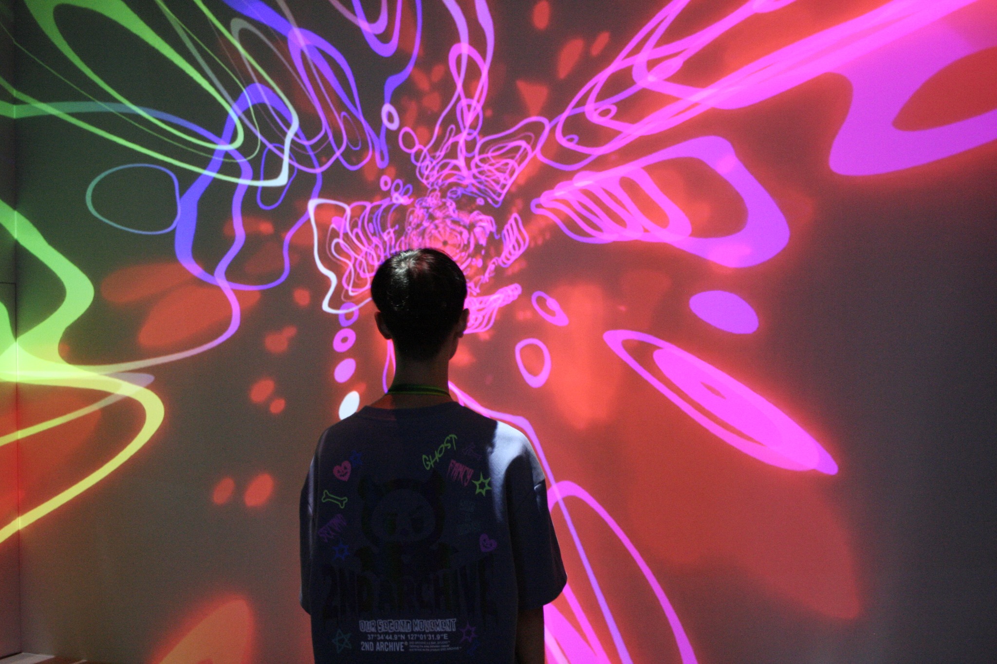
The two experimental sessions are Prof. Hoang-Yan Lin's "XR Display Technology and Applications in Metaverse" and Prof. Ding-Wei Huang's "Multi-viewzone Optical Thin Film and Image Design." The former focuses on virtual reality, simulating the human vision, allowing the user to feel as if they are personally inside the virtual world, able to freely observe the virtual world. When the user position changes, the computer performs complex calculations to provide accurate images of the 3D world in real time. Compared to conventional planar display, wearing VR glasses allows the user to be more immersed in the virtual world. The experiments demonstrate the difference between using conventional display screens and wearable VR devices, and provide three different usage scenarios, to demonstrate the immersiveness on different levels.
|
 |
 |
|
Fig. 1. Experiencing VR through VR glasses |
Fig. 2. The students and Prof. Hoang-Yan Lin |
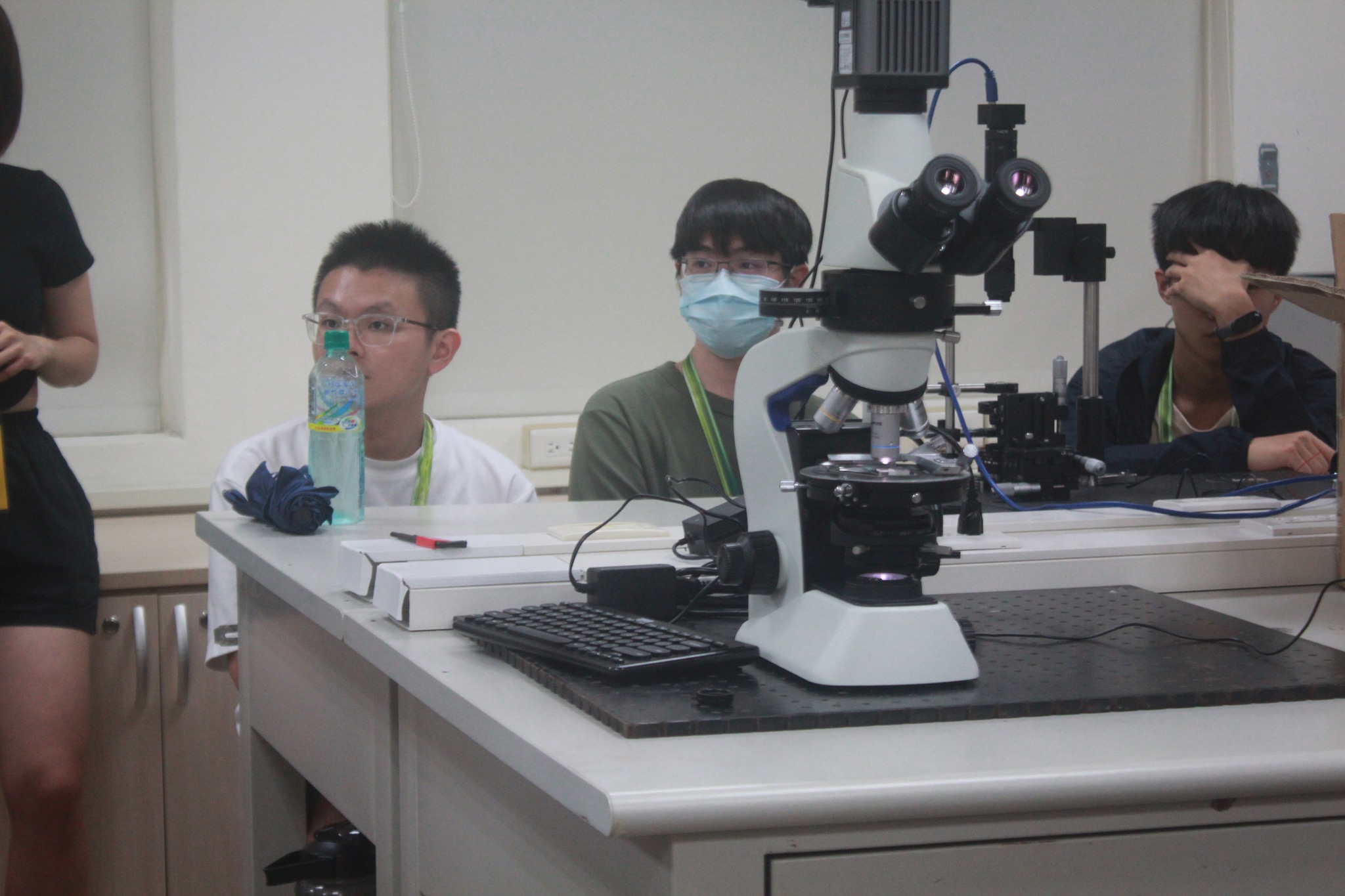
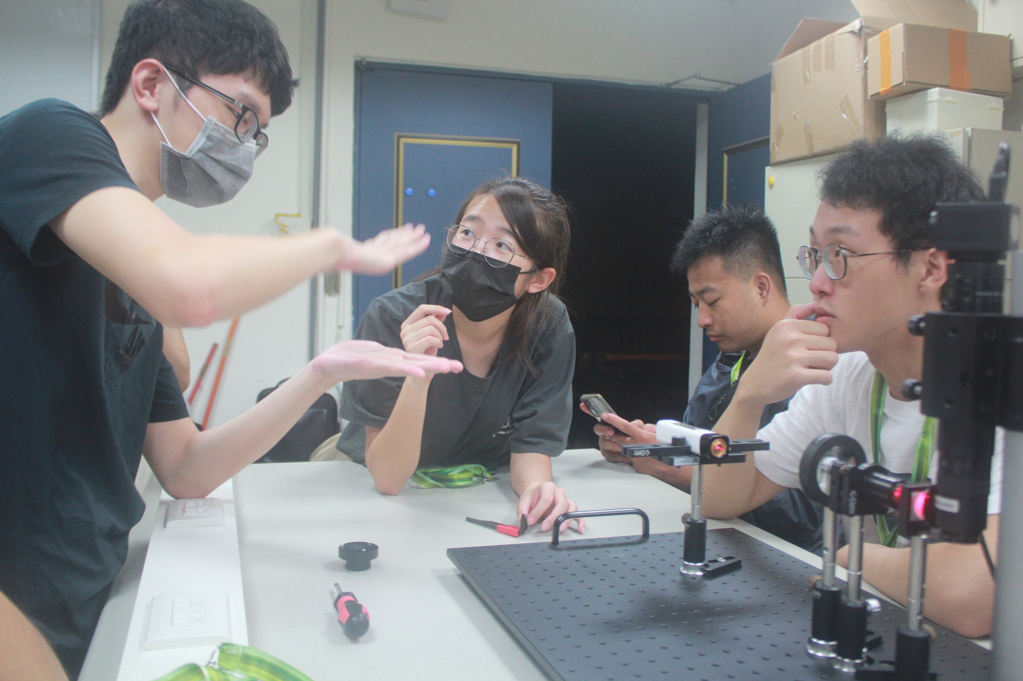
The latter utilizes optical grating to create images. An optical grating is an optical device with repetitive lines or patterns, typically in the shape of parallel grooves and lines. They can be used to disperse or focus light to create specific optical effects. In the experiment, a computer software is used to demonstrate the creation of images, from two or more images, then viewing the composite image through the gratings. The width of the gratings will have an effect on the viewed image.
|
 |
 |
|
Fig. 3. Prof. Ding-Wei Huang explains the experiment |
Fig. 4. The students operating the software |
On the second day, the group leaders first called the groups in for a discussion, followed by a seminar given by Prof. Hsiang-Chieh Lee and Prof. I-Chun Cheng. Prof. Hsiang-Chieh Lee gives us an introduction on "Biomedical Optoelectronics" and its applications, and Prof. I-Chun Cheng talks about "Flexible Display Technology," covering a diverse range of topics.
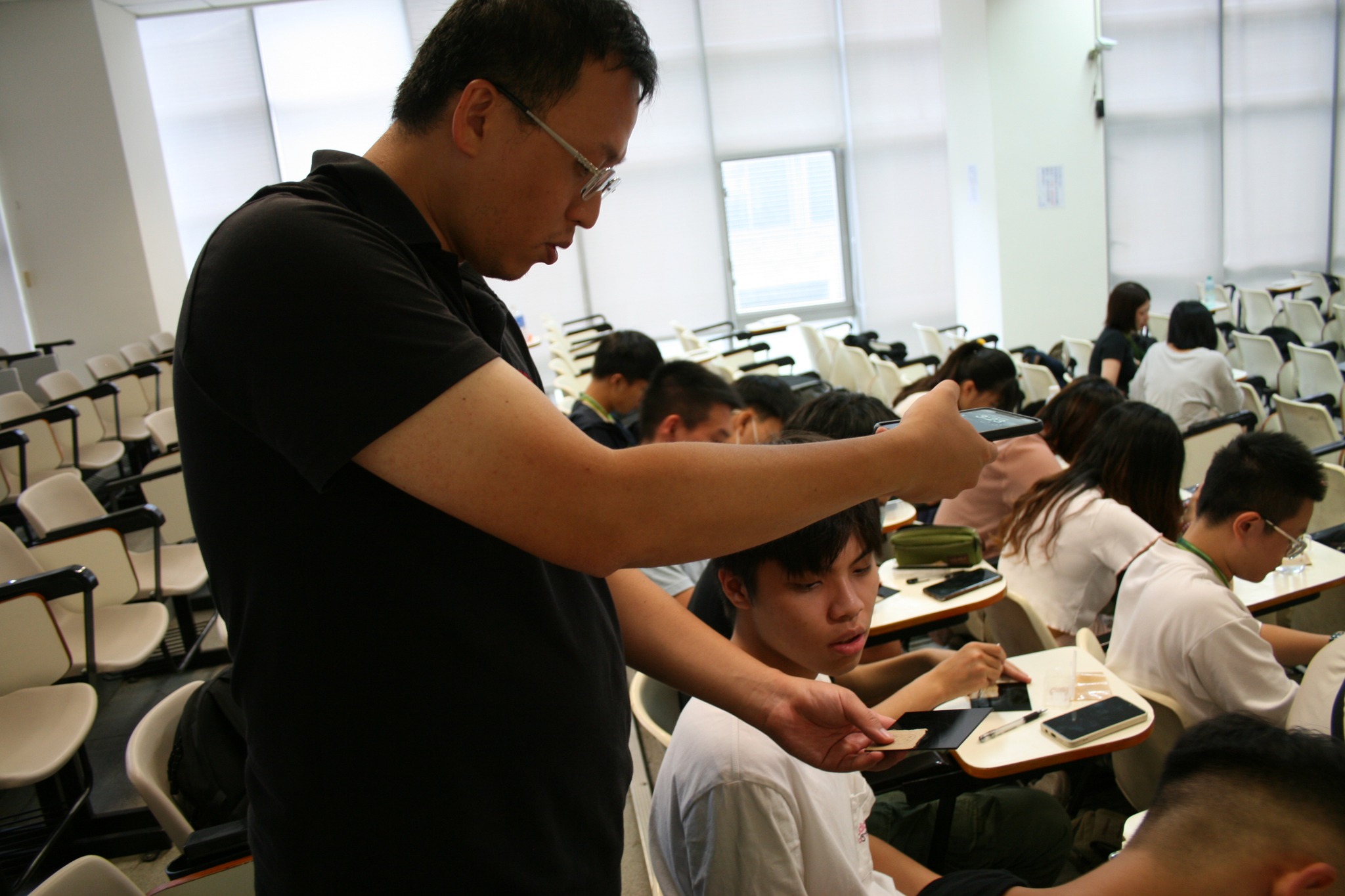
In the afternoon, like the first day of the camp, are two arranged experiment sessions. Prof. Lung-Han Peng's "Jewelry Appraisal and Cone Projection and Newton Ring Interference" is a demonstration of the amazing wonderful properties of light. Planar-convex lenses and planar glass plates are stacked and placed underneath a light source, and at a distance beautiful rings of prismatic colors can be observed. These rings radiate outward with the light source at their center, forming beautiful annular patterns from the effects of refraction and diffraction. In the process, students can observe the refraction of light between different optical media, which leads to the formation of optical path difference, which leads to formation of the interference pattern. By observing the size and colors of the rings, the effect of the thickness of the air gap can be deducted, and is a wonderful demonstration of the connection between theoretical knowledge and practical operations.
|
 |
 |
|
Fig. 5. The students and Prof. Lung-Han Peng |
Fig. 6. The staff members answering questions |
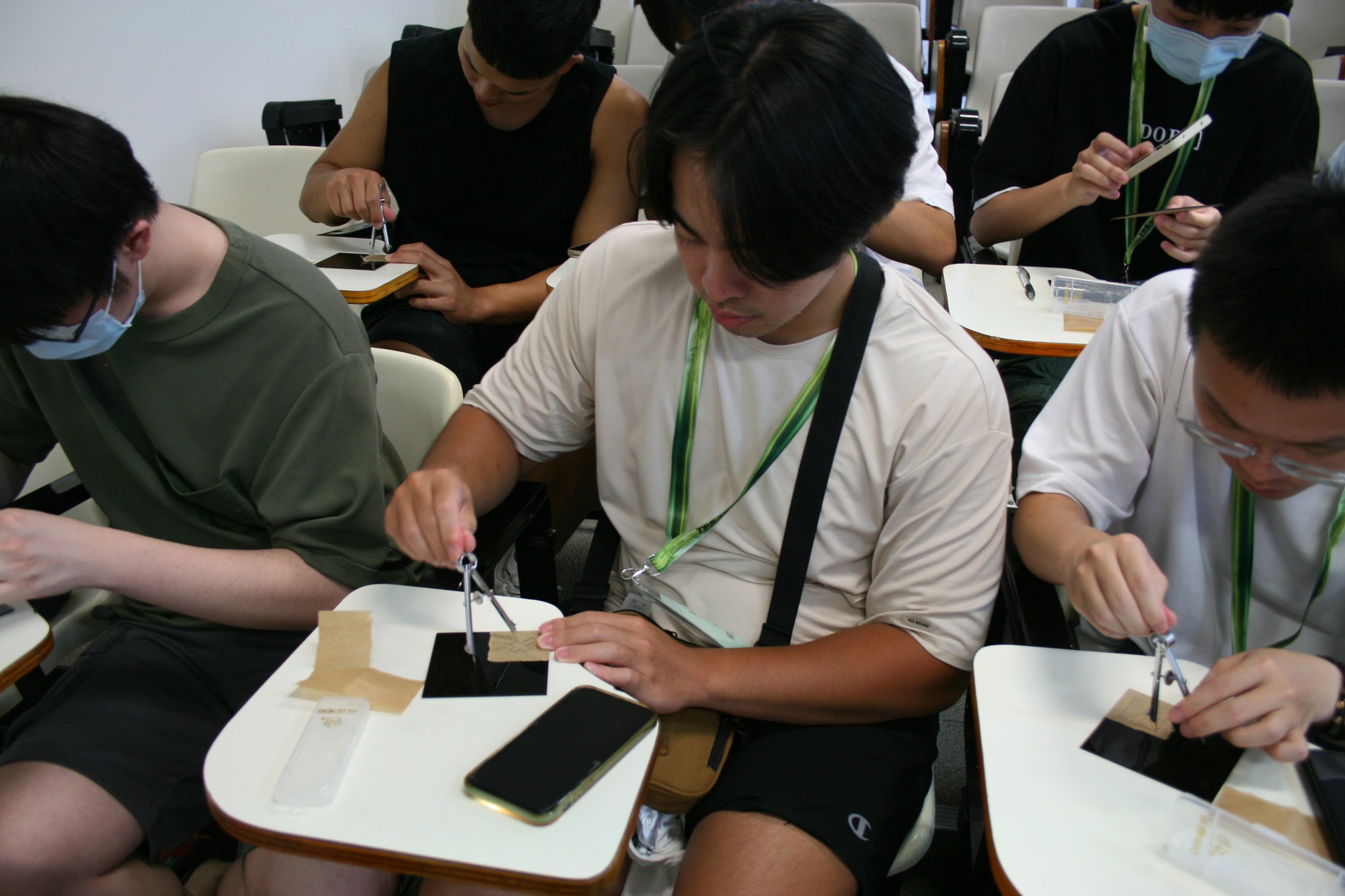
Prof. Yu-Hsiang Cheng's "Scratch Hologram" is a simple and yet extremely intriguing experiment. As directed by Prof. Cheng, the students shone light from a LED through a scratched plate onto a light sensitive material, which forms an interference pattern. The apparatus is secured, so the exposure and development can be performed in a stable environment, and the result is a hologram image containing the 3D information of the scratch. Through taking advantage of the interference of light, small and fine details can be captured. This is an amazing demonstration of the wave interference of light and its diffraction property, and how they can be used in the creation of holographic images.
|
 |
 |
|
Fig. 7. Prof. Yu-Hsiang Cheng assisting the students in the experiment |
Fig. 8. The students making scratches on the plate |
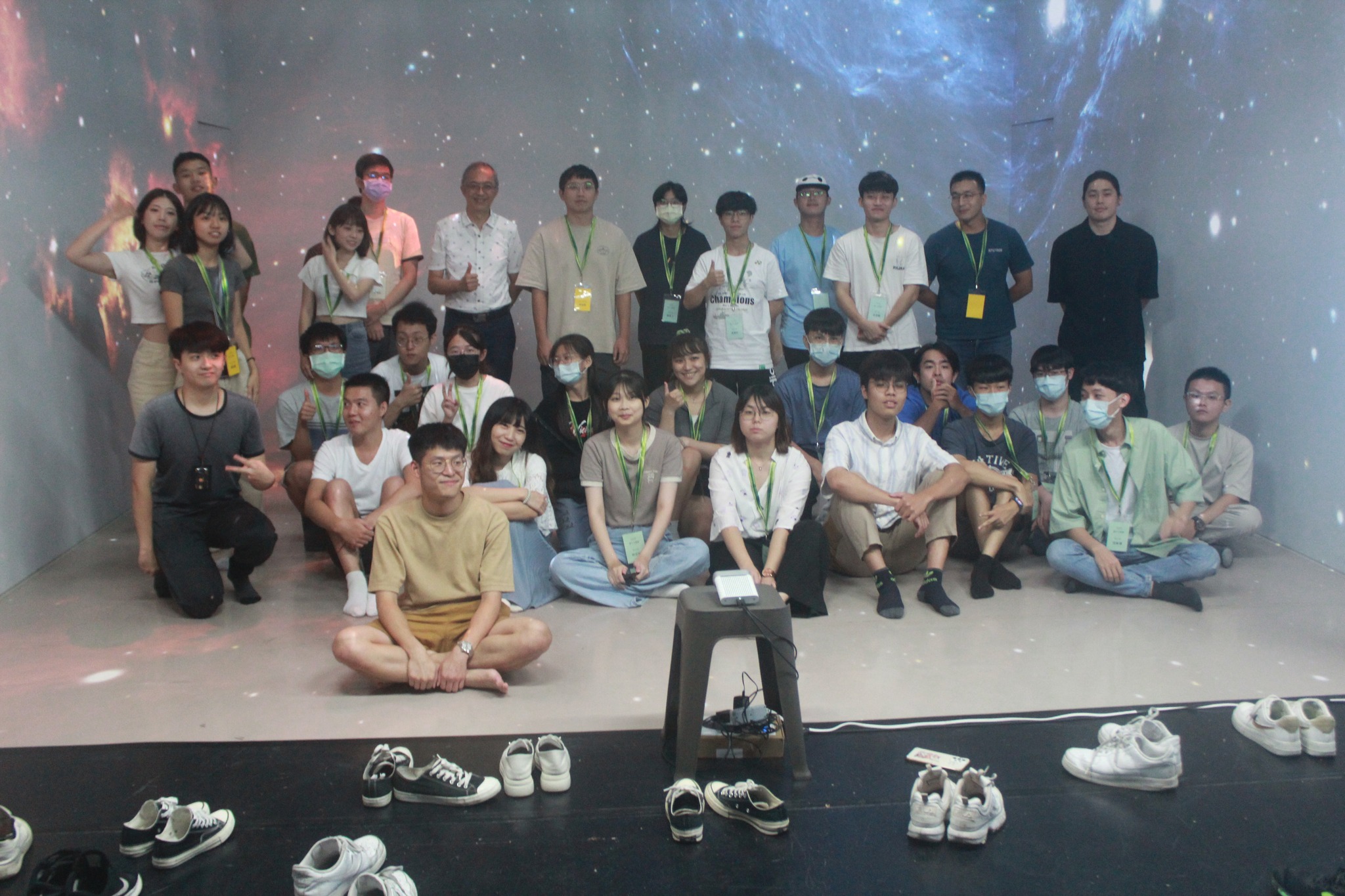
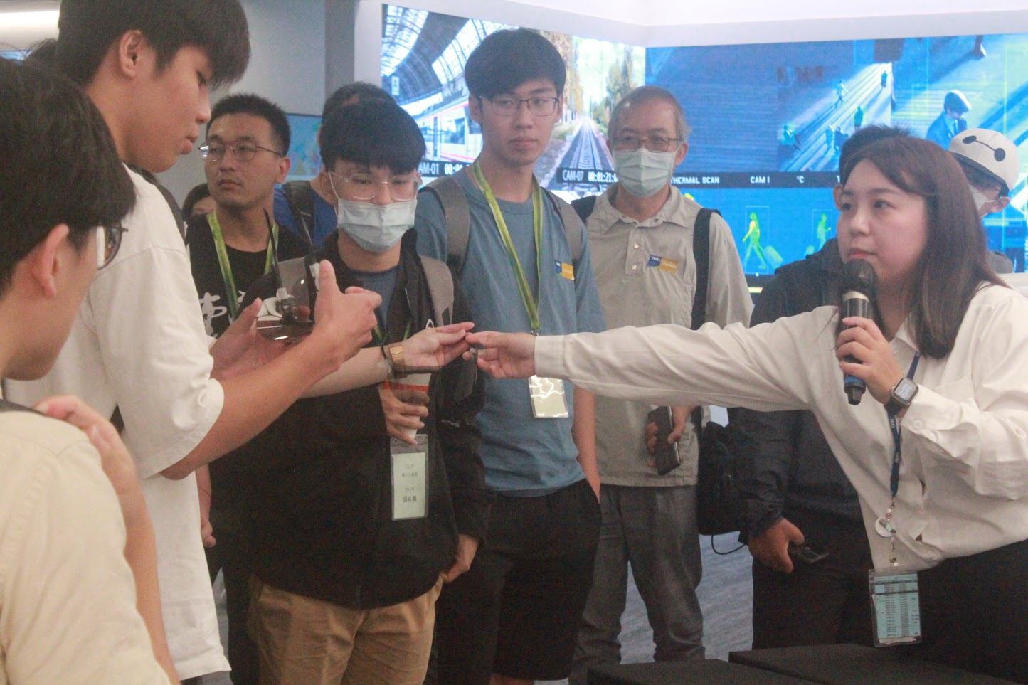
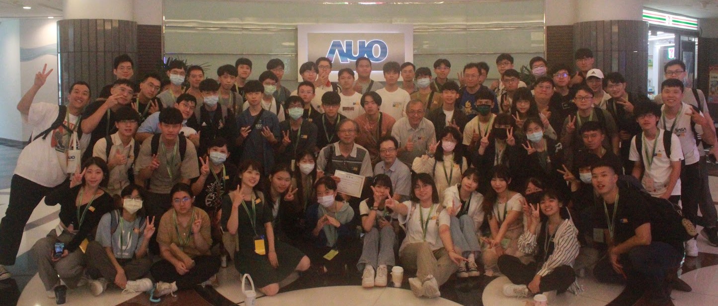
Lastly, on the third day, the camp takes place at AUO headquarter at Hsinchu. Due to the travel time, the trip is confined to a tight schedule. Upon arrival, the Vice Manager Kun-Cheng Tien of the RD department welcomes us and shares with us his experiences in the industrial fields, and takes us for a tour at the newly constructed apprenticeship workshop. The engineers and professionals at AUO guide and explain to the students a brief understanding of the fabrication of photonics and electronics devices, then present a themed showroom demonstrating optoelectronics applications utilized in various scenarios, such as tourism transportation, restaurant bar, clinical operation room and consultation rooms, demonstrating the many uses and advantages of various types of display technology. Throughout the tour the students are kept in a wide eyed wonder, perhaps other than learning the theoretical fundamentals, also seeing and experiencing the technologies personally enables the students to have a clearer understanding and outlook in the future.
|
 |
 |
|
Fig. 9. Guided tour through the showroom |
Fig. 10. Chairman Prof. Yuh-Renn Wu expresses gratitude and acknowledgement to AUO for their support |
|
 |
|
Fig. 11. Group photo at the lobby |
|
|
|
|
|
|
|
|
|
| |
|
|
|
|
|
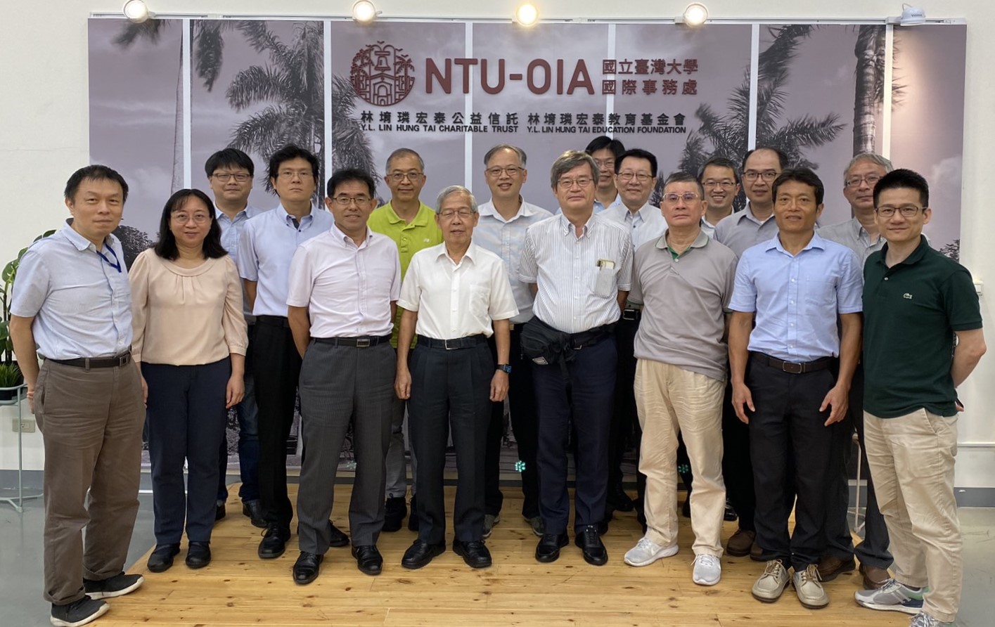
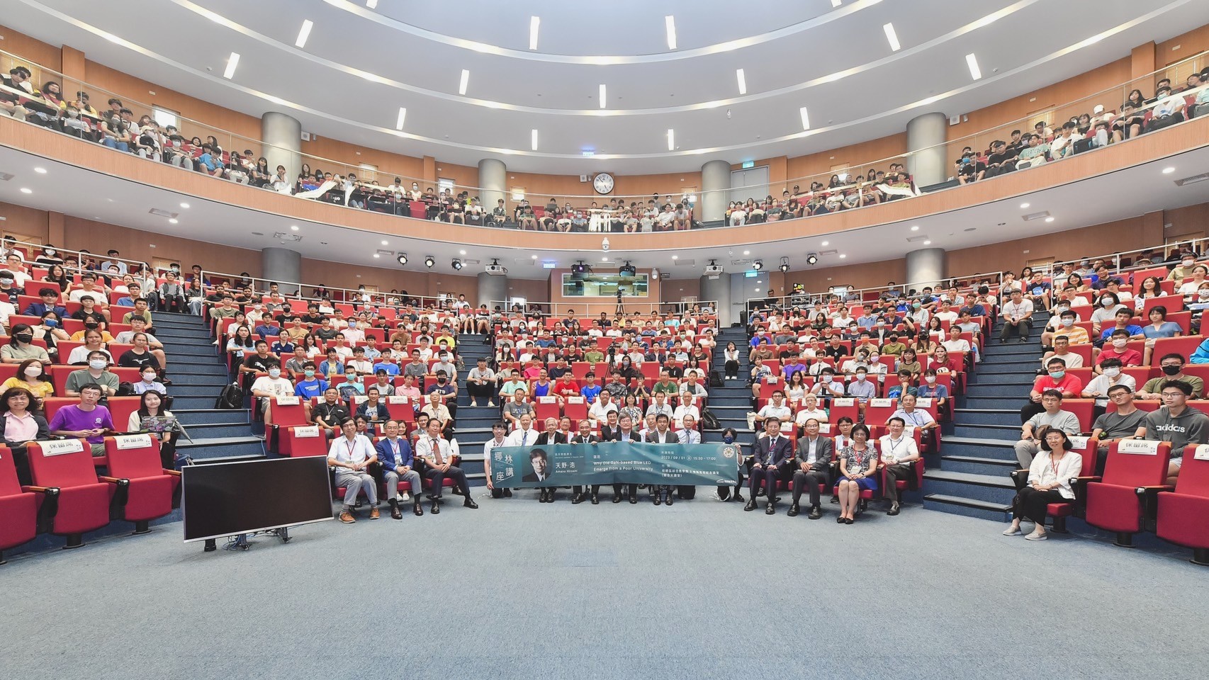
~ Academic Visitation - Prof. Hiroshi Amano (Nobel Laureate 2014) ~
(September 1, 2023, NTU Shih-Liang Chien Lecture Hall)
(September 2, 2023, Complex for Research Excellence, NTU Shuiyuan Campus)
By Hsiao-wen Lin
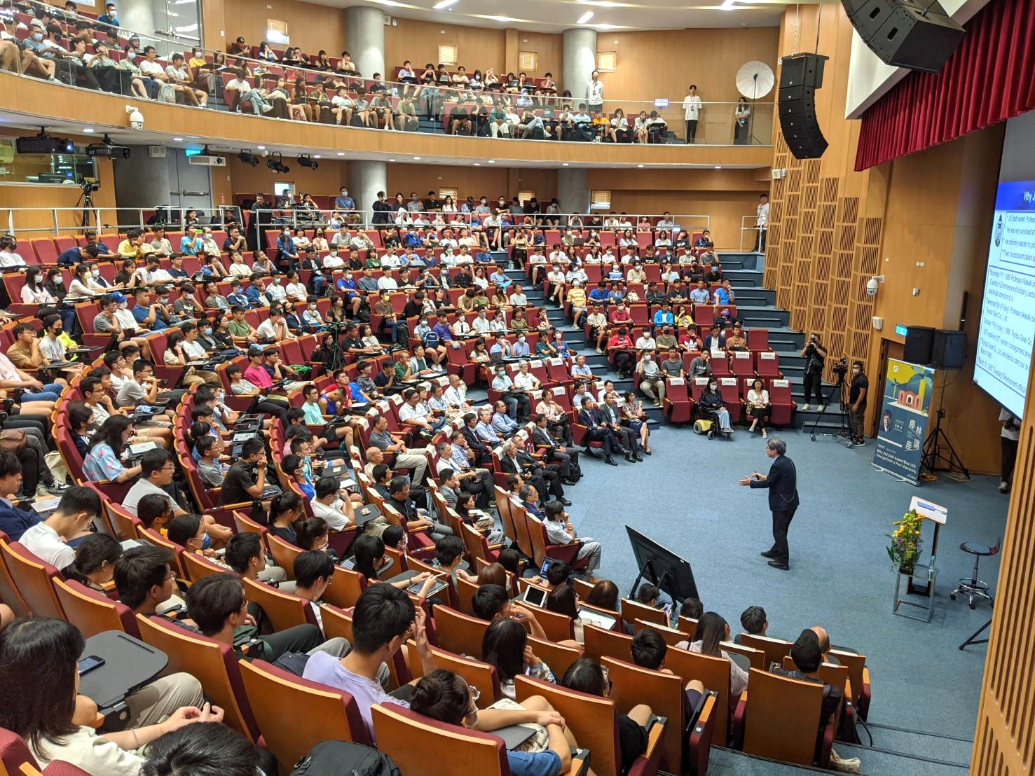
This year, the National Taiwan University has decided to initiate a new seminar series, the Royal Palm Lecture Series, inviting influentials in both the academic fields and industrial fields from all across the globe to NTU to share their brilliance with the people of NTU. On the day of Sep. 1st, 2023, we have the honor of receiving the holder of the Nobel Physics Prize of 2014, Prof. Hiroshi Amano, to hold the first seminar, with the topic "Why did GaN-based blue LED emerge from a poor university." In the past on Dec. 19th, 2014, the GIPO had once invited Prof. Amano to give a talk to our students, and what a wonderful coincidence that we once again have the honor of receiving Prof. Amano again today.
Currently a Distinguished Professor of Nagoya University, Japan, Prof. Amano is a famous and accomplished engineer. In the year of 2014, together with Prof. Isamu Akasaki of Nagoya University and Prof. Shuji Nakamura of UC Santa Barbara, USA, the three of them jointly received the Nobel Physics Prize for "the invention of high intensity blue LED, to bring about an energy saving high intensity white light source."
Incidentally, Prof. Amano's visit attracts so much attention campus wide that upon the seminar notice announcement, the online enrollment system quickly reaches peak capacity of 500 participants and requires opening up the reserved synchronized lecture room to accommodate for the overflowing number of participants. On the day of the seminar, more than 600 participants including students and teachers come to listen and witness this memorable event together. In the seminar, Prof. Amano shares and walks through with us his thoughts and his feelings as he began to walk down the path of his research and careers, and the crucial importance of "Persistence," "Enthusiasm," and the "Vision of Future." Prof. Amano encourages the students to search and find for themselves these characters, and concludes the seminar with, "And now, it is your turn! Do not let the talents that each and every one of you have within you go to waste!"
|
 |
|
 |
To take advantage of such a wonderful occasion, with the permission of Prof. Amano, on the day after the seminar the GIPO holds another cross-departmental conference, inviting professors from a range of related fields from the school of science to the school of engineering to the school of information to come and exchange thoughts and ideas with Prof. Amano and his colleague Prof. Arai in an easy going and casual atmosphere, and we all have a wonderful time extending to the lunch banquet that followed, which makes us look forward all the more to the next time that we meet again.
|
|
|
|
|
|
|
|
|
| |
|
|
|
|
|
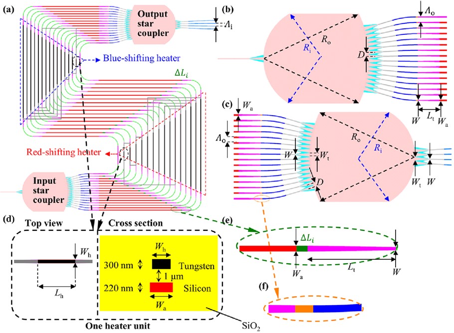
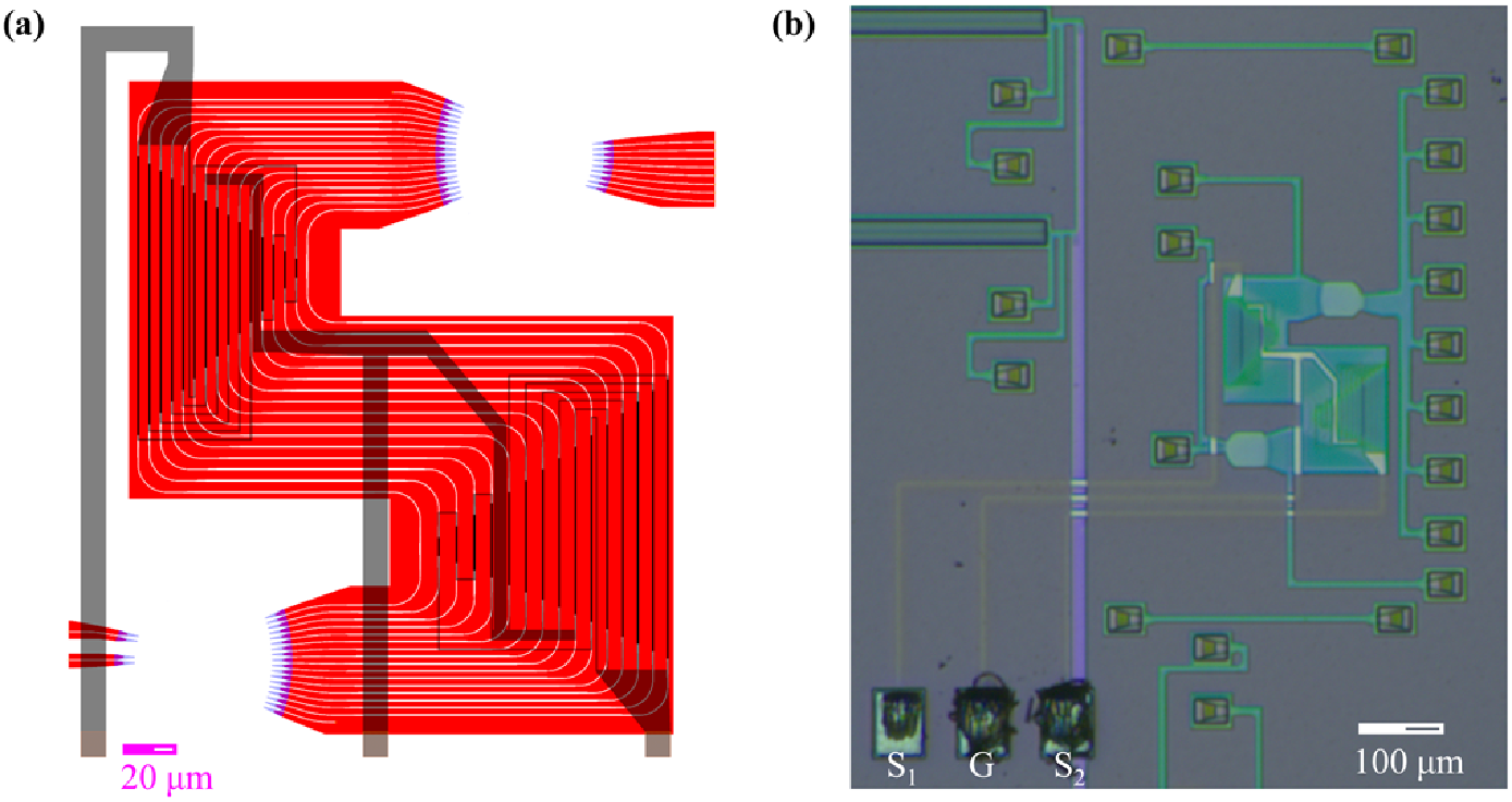
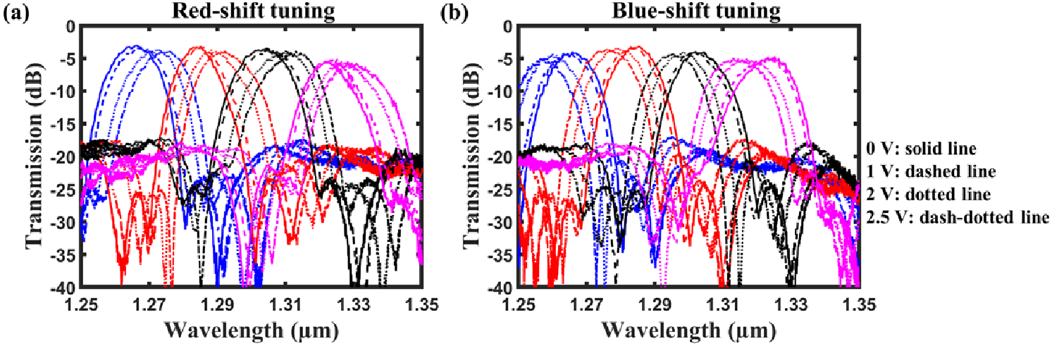
Bi-directionally Tunable Arrayed Waveguide Grating with Ultra-low Thermal Power
Professor Ding-Wei Huang
Graduate Institute of Photonics and Optoelectronics, National Taiwan University
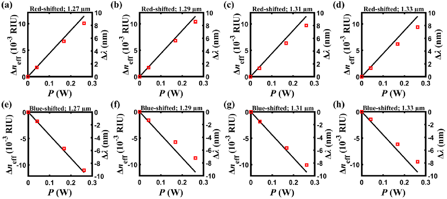
A thermally bi-directionally tunable arrayed waveguide grating (TBDTAWG) is proposed and demonstrated on a silicon-on-insulator (SOI) platform (Fig. 1). The device is composed of passive and active designs for realizations of an AWG and fine tuning of its filtering responses. Given that the required length difference between adjacent arrayed waveguides for the SOI platform is considerably short (∼3–5 µm) due to a high index contrast, an S-shaped architecture with a larger footprint instead of a rectangular one is employed in the AWG (Fig. 2). Bi-directionally tunable functions, i.e., both red- and blue-shift tunable functions, can be achieved by using two triangular thermal-tuning regions with complementary phase distributions in the S-shaped architecture despite using only materials with positive thermo-optic coefficients, i.e., Si and SiO2. Measurement results illustrate that both red- or blue-shifted spectra can be achieved and a linear bi-directional shift-to-power ratio of ±30.5 nm/W as well as a wide tuning range of 8 nm can be obtained under an electrical voltage range of 0–2.5 V, showing an agreement between the measurement results and two-dimensional simulation results (Figs. 3 and 4). This also shows the potential of the proposed TBDTAWG for automatically stabilizing the spectral responses of AWG-based (de)multiplexers for coarse or dense wavelength division multiplexing communication systems by using a feedback control circuit.
|
|
|
Fig. 1. Schematic top view of (a) overall TBDTAWG, (b) input star coupler, (c) output star coupler, (d) magnified top view and cross section of one heater unit, (e) magnified length difference (dark green), and (f) magnified straight waveguide (orange).
|
|
|
|
Fig. 2. (a) Mask layout of the proposed TBDTAWG and (b) photograph of the fabricated device on the SOI chip.
|
|
|
|
Fig. 3. (a) Red-shifted and (b) blue-shifted filtering responses for different applied voltages of 0, 1, 2, and 2.5 V are represented by solid, dashed, dotted, and dash-dotted lines, respectively.
|
|
|
|
Fig. 4. The linear relationship between the spectrum shifts and the required thermal powers at four output Channels 1.27, 1.29, 1.31, and 1.33 µm for (a–d) red-shift tuning and (e–h) blue-shift tuning, where the solid line and squared red marker represent the simulated results from Fig. 4 and the measured data from Fig. 6, respectively.
|
Design and Realization of a Wide Field-of-view Scanning LiDAR Based on MEMS Mirror
Professor Guo-Dung Su
Graduate Institute of Photonics and Optoelectronics, National Taiwan University
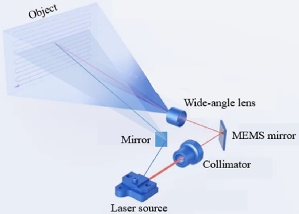
Light Detection and Ranging (LiDAR) sensor technology is the main driving force for automated transportation. Through the fusion of LiDAR sensor data, radar and camera lens, the surrounding environment can be fully and robustly sensed. However, most of today's LiDAR solutions are very complex and costly, and cannot effectively achieve scanning with a large field of view, so they cannot be widely used in vehicles and robots. We simulated and demonstrated a complete LiDAR system to solve the current obstacles to the development of MEMS LiDAR. By combining a MEMS mirror and a wide-angle lens into the scanning system, a low-cost, small-volume, and large-field-of-view LiDAR system can be realized. First, use ZEMAX OpticStudio optical simulation software to design a group of aspherical optical systems on the basis of scanning and widening optics to achieve the purpose of expanding the scanning angle of light. After the laser beam passes through this group of wide-angle lenses, the scanning angle can be expanded 4 times to 100 degrees. The distortion of the wide-angle lens is controlled below 3%, making the scanned image closer to the real situation. Second, in order to demonstrate low-cost, small-volume MEMS scanning LiDAR, a modular laser rangefinder (LRF) is used and a MEMS mirror is added. The entire system is erected on a self-designed and manufactured support. The complete prototype of LiDAR scanner is less than 150mm×50mm×30mm. The weight is less than 250 grams. In the 2klux natural light environment for wide-angle LiDAR measurement and analysis, the maximum error is 4.1cm, so the error is within 2%. Finally, a self-written image processing program was used to convert the scanned data into a 3D point cloud image, and the generated image proved the complete function of LiDAR.
|
|
|
Fig. 1. Combining an off-shelf single-point range finder, a MEMS mirror, and a wide-angle lens into the system, small-volume and large field-of-view (FOV) LiDAR systems can be realized.
|
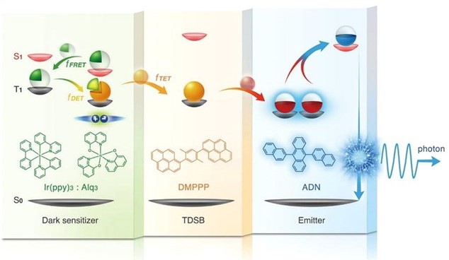
Phosphor-doped fluorophore as dark sensitizer for blue triplet-triplet annihilation upconversion organic light-emitting diode
Professor Jiun-Haw Lee
Graduate Institute of Photonics and Optoelectronics, National Taiwan University
By doping 8% green phosphor, tris[2-phenylpyridinato-C2,N]Iridium(III) (Ir(ppy)3), into green fluorophore, tris-(8-hydroxyquinoline)aluminum (Alq3), a dark sensitizer (DS) was achieved for a blue organic light-emitting diode, consisting of triplet-triplet annihilation (TTA) emitter, 9,10-bis(2’-naphthyl) anthracene (ADN). Carriers recombined at Alq3 molecules which formed 25% singlets and 75% triplets. 25% Alq3 singlets underwent intersystem crossing to Ir(ppy)3 triplets followed by triplet energy transfer (TET) to Alq3 triplets, which resulted in 100% triplets in total, for TTA process which generate efficient blue emission. No fluorescence emission from green sensitizer was observed which efficiently improved external quantum efficiency of blue emission.
Manipulation of plasmonic relaxation possible by voltage-modulation
Professor Jian-Jang Huang's Laboratory
Graduate Institute of Photonics and Optoelectronics, National Taiwan University
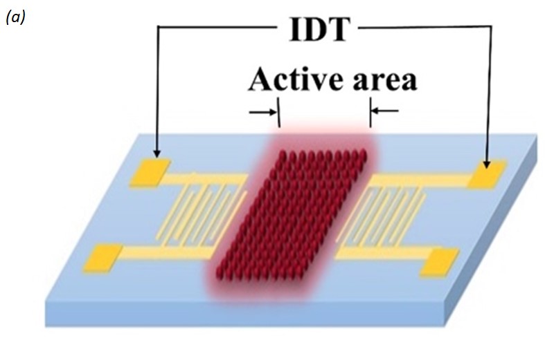
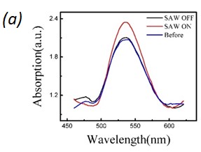
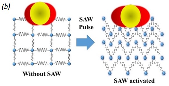
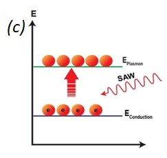
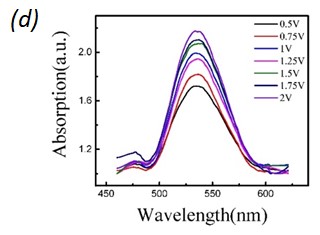
We experimentally study the effect of amplitude varying surface acoustic waves on localized surface Plasmon (LSP), which unveils exceptional properties of plasmon-phonon interaction with promising applications in future tunable photonic devices. Gold nanoparticles are deposited on an X-cut LiNbO3 to generate plasmonic oscillation, and an interdigital transducer is fabricated to create surface acoustic wave pulses. The interaction between amplitude varying mechanical wave and plasmonic oscillation affects different plasmon dynamics and relaxation gradients, leading to a systematic change in LSP absorption. We also demonstrated the effect of polarized light on the device, providing a unique characteristic to explore the manipulation process effectively.
|
|
|
|
Fig. 1. (a) Illustration of the device, which is composed of a source IDT, randomly distributed Au nanoparticles and a receiving IDT. (b) (i) (ii) (iii) SEM images of fabricated IDT, (iv) Surface morphology captured by SEM where 40nm uniformly sized Au nanoparticles are distributed on the surface.
|
|
|
|
|
|
|
|
|
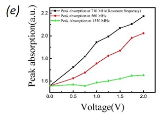
Fig. 2. (a) LSPR response with respect to different switching conditions of the IDT. Where the LSPR adsorption increase with SAW is On and retract back when SAW is off. (b) Diagram of phonon-plasmon interaction with and without SAW activated acoustic phonons. The plasmonic electron density increases with the applied SAW pulse as compared to the case without SAW. (c) Illustration of SAW activated electron transition to the plasmonic state. The SAW activated phonons participate in phonon-plasmon coupling and increase the plasmonic population. (d) Change of LSPR absorption with varying amplitude of SAW. (e) Amplitude varying LSPR response with respect to different SAW resonant conditions, where at the SAW resonant frequency (710 MHz) the change of LSPR absorption is highest.
|
Low-Temperature HfZrO2 Ferroelectric Thin-Film Transistors with a-InGaZnO Channels
Professor I-Chun Cheng
Graduate Institute of Photonics and Optoelectronics, National Taiwan University
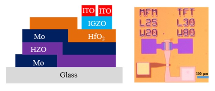
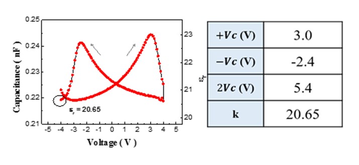
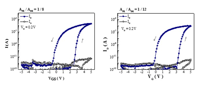
Owing to the relatively low process temperatures, HfO2-based ferroelectric materials integrated with oxide-based thin-film transistors have been considered as potential candidates for back-end-of-line compatible ferroelectric field-effect transistors, which can be vertically stacked on silicon CMOS circuits to realize high-density neural network applications or implemented on various types of substrates for novel applications. It is known that the formation of ferroelectric orthorhombic phase in HfO2-based materials can be strongly influenced by the annealing temperature, the thickness of film and the types of top and bottom metallic electrodes. In this work, low-temperature ferroelectric thin-film transistors (Fe-TFTs) were developed by monolithically integrating HfZrO2 (HZO) ferroelectric capacitors with amorphous indium gallium zinc oxide (a-IGZO) TFTs on glass substrates. Figs. 1(a) and (b) show the schematic diagram and microscopic photograph of the on-glass FeTFT, respectively. The Fe-TFT has a metal-ferroelectric-metal-insulator-semiconductor structure. The HZO ferroelectric layer was deposited by atomic layer deposition. The a-IGZO channel layer was deposited by rf-sputtering. The maximum process temperature is 350°C. A butterfly-shaped capacitance-voltage curve is observed, as shown in Fig. 2, revealing the top and bottom Mo electrodes can introduce sufficient mechanical stress to induce the formation of ferroelectricity in the HZO layer after annealed at 350°C. The positive and negative coercive voltages are 3 V and -2.4 V, respectively. The dielectric constant is 20.65. Fig. 3 shows the transfer hysteresis curves of the low-temperature HZO Fe-TFTs. The Fe-TFTs exhibit large hysteresis memory windows of 2.8 V and 3.8 V when the area ratios between ferroelectric capacitors and gate insulators are 1/8 and 1/12, respectively.
|
|
|
|
Fig. 1. (a) Schematic diagram and (b) optical micrograph of HZO Fe-TFT with a-IGZO channel.
|
Fig. 2. Capacitance-voltage curve & dielectric constant of low-temperature annealed HZO ferroelectric capacitor.
|
|
|
|
Fig. 3. Transfer hysteresis curves of HZO FeTFTs with (a) AFE / ADE = 1 / 8 and (b) AFE / ADE = 1 / 12. The Fe-TFTs are operated at VDS = 0.2 V.
|
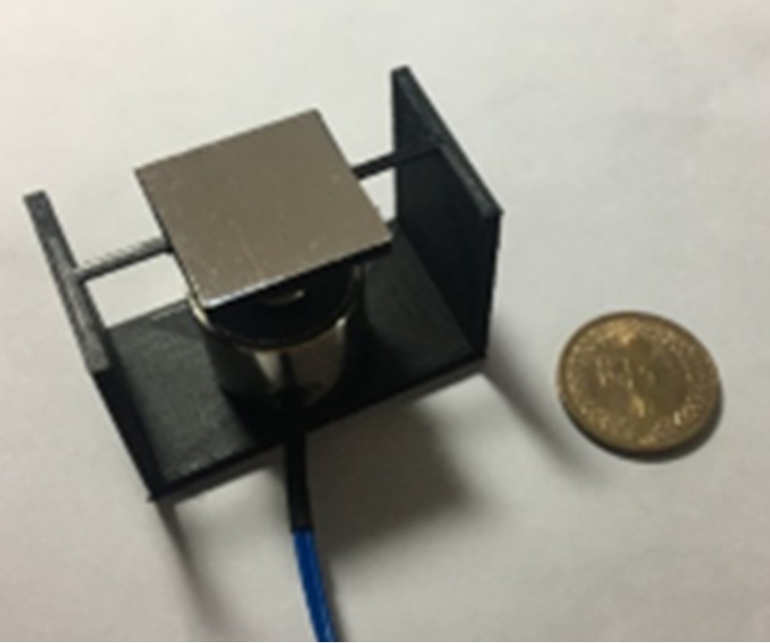
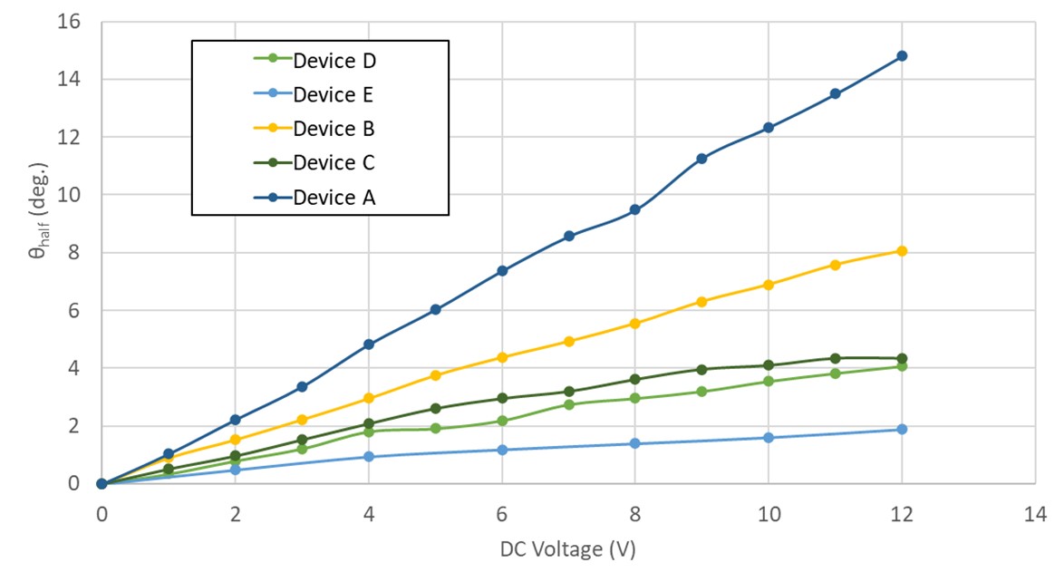
Low-Cost 3D-Printed Large-Area 1-DOF Scanners
Professor Jui-che Tsai
Graduate Institute of Photonics and Optoelectronics, National Taiwan University
We have developed 3D-printed 1-DOF (one torsional axis; 1 degree of freedom) optical scanners with large mirror areas (up to 20 × 20 mm2). Each device consists of an aluminum-coated square silicon substrate serving as the mirror, two miniature permanent magnets, an electromagnet, and a 3D-printed structure including the mirror frame, torsion springs, and base. One device can reach a static half optical deflection angle of 14.8 deg. at 12 VDC; this particular device exhibits a mechanical resonance frequency of 84 Hz. These scanners can be a potential, low-cost alternative to the expensive conventional galvanometer scanners.
|
(a)
|
(b)
|
|
|
|
|
Fig. 1. (a) Device with a 20 × 20 mm2 mirror area (Device A). (b) Static characteristics: optical half angle θhalf vs. dc voltage for different devices.
|
Shen, C.-K.; Huang, Y.-N.; Liu, G.-Y.; Tsui, W.-A.; Cheng, Y.-W.; Yeh, P.-H.; Tsai, J.-c.*, “Low-Cost 3D-Printed Electromagnetically Driven Large-Area 1-DOF Optical Scanners,” Photonics, vol. 9, no.7, 484, Jul. 2022.
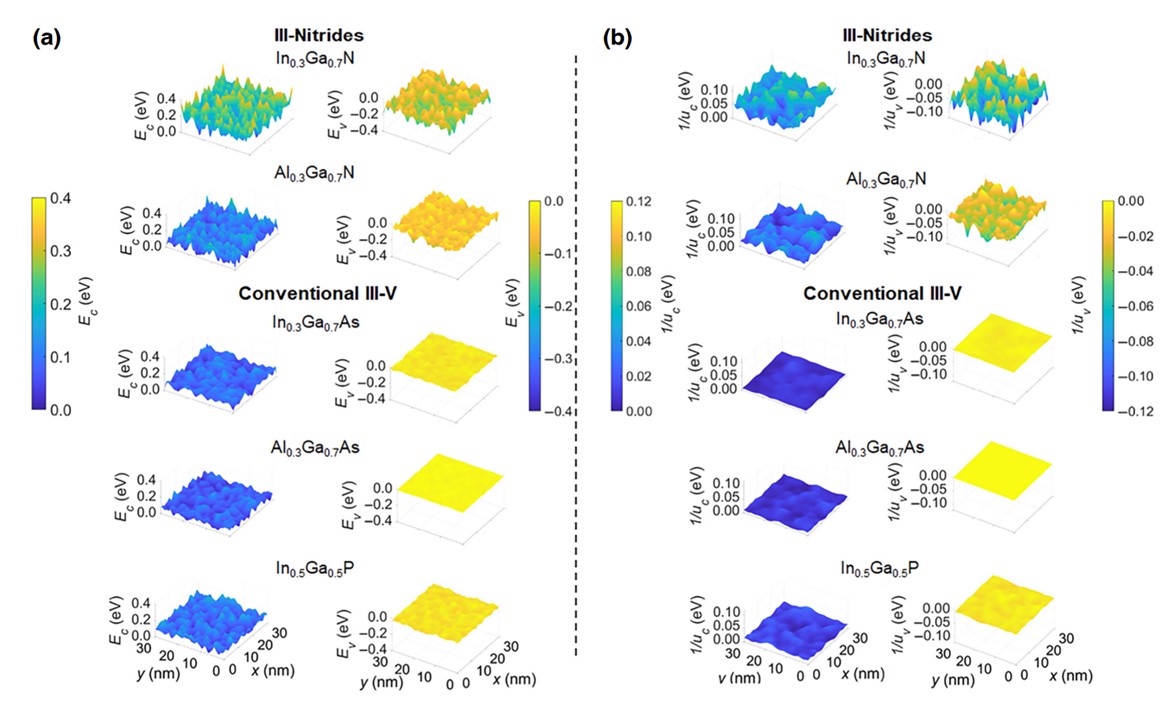
Carrier localization in III-nitride versus conventional III-V semiconductors: A study on the effects of alloy disorder using landscape theory and the Schrödinger equation
Professor Yuh-Renn Wu's
Laboratory
Graduate Institute of Photonics and Optoelectronics, National Taiwan University
Semiconductor devices often necessitate the practice of band-gap engineering, a process that involves the utilization of alloys and the fine-tuning of their composition to achieve the desired electrical or optical characteristics. While deviations in composition are typically considered minor perturbations in conventional III-V semiconductors, the impact of alloy disorder is significantly more pronounced in III-nitrides. This study aims to compare the influence of alloy disorder on carrier localization, focusing on various III-V semiconductors, particularly with regard to holes, where localization effects are more pronounced due to their greater effective mass.
To conduct this investigation, we employ three-dimensional computational methods for III-V alloys featuring natural (random) compositional fluctuations. Given the intricacy of the problem, our computations are based on a simplified Hamiltonian within the envelope wave-function approximation, focusing on a single heavy-hole valence band. We explore the impact of compositional fluctuations on carrier localization using two distinct approaches.
The first approach leverages the localization landscape theory, allowing us to solve the localization landscape equations and derive the effective potentials that act upon carriers. These potentials serve as confining forces, predicting the spatial regions where carriers are most likely to be localized. This enables a comparative analysis of the effects of alloy fluctuations between conventional III-V and III-nitride semiconductors. Notably, we observe that the effective potential in III-nitride semiconductors exhibits considerably larger fluctuations compared to other III-V semiconductors, potentially indicating a higher degree of carrier localization in nitrides, particularly for holes.
To validate this observation, we employ the second method, solving Schrödinger's equation to determine the electron and hole wave functions. Our findings reveal that in InxGa1−xN, electron wave functions tend to be delocalized, even in the ground state, while low-energy hole states exhibit localization. This contrasts with the behavior of holes in the common alloy InxGa1−xAs, where they are consistently found to be delocalized. Thus, our study underscores the significance of accounting for alloy disorder in nitride semiconductors.
This work is published in Phys. Rev. Applied, 20, 044069 (2023).
DOI: 10.1103/PhysRevApplied.20.044069
|
|
|
Fig. 1. (a) 2D sectional maps of CBM and VBM for different semiconductor alloys in an x-y plane in the middle of the structure. Maps of compositional fluctuations are not shown as they are the same for random alloys with the same relative composition (30% here), except for In0.5Ga0.5P with 50% composition. The zero-energy references for Ec and Ev are, respectively, the minimum and maximum values of band extrema for a specific realization. (b) 2D cross sections of the corresponding effective potentials computed by the LL equations. Compare the size of effective energy fluctuations with those of the originating band extrema energy fluctuations (note the different energy scales). The left and right color bars correspond to each column of the sectional maps.
|
|
|
|
|
|
|
|
|
|
|
|
 |
|
 |
|
|
|
|