|
Fully electromagnetic wave optic simulation and analyses of the cross-scale reflective 3D emissive pixel configuration for displays
Professor Chung-Chih Wu
Graduate Institute of Photonics and Optoelectronics, National Taiwan University
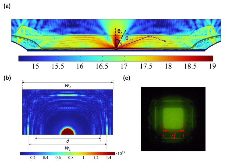
To enhance optical out-coupling and power efficiency of light-emitting diode displays, a reflective three-dimensional (3D) pixel structure had been reported previously. The multi-scale optical simulation combining wave and ray optics used for optical modeling of such cross-scale structures in the previous work, although more effective in computing time and resources, was not able to treat all detailed emission properties. In our study, by reducing the computing load to a feasible scale via refining the meshing, symmetry simplification and a few other strategies, we successfully conducted the full electromagnetic wave optics simulation of the cross-scale 3D light-emitting pixel structure and used it to treat all detailed emission properties (either spectrally integrated or wavelength resolved). The reported simulation approach and strategy shall provide a useful guide for handling similar cross-scale numerical electromagnetic wave optics simulation.
|
|
|
Fig. 1. (a) The x-z-plane cross section of the radiating power density flux (i.e., the Poynting vector magnitudes) from the single-frequency y-direction dipole located at the center of the active emission region. qint is the initial internal angle of radiation coupled from the OLED into the high-index filler region and qc is the TIR (total internal reflection) critical angle of the filler-air interface. (b) The z component of the Poynting vector on the topmost (receiving) surface in air for radiation from dipoles (all x-, y-, and z-direction dipoles together) at the center of the active emission region. (c) The EL image of the reflective 3D pixel taken with the optical microscopy.
|
MoS2 as Effective Cu Diffusion Barriers with Back-End Compatible Process
Professor Chih-I Wu
Graduate Institute of Photonics and Optoelectronics, National Taiwan University
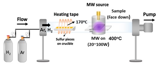
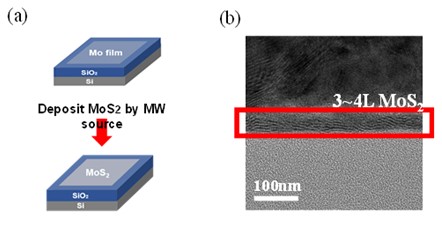
The previous researches showed that MoS2 growth methods, such as high temperature CVD and Plasma Enhance Chemical Vapor Deposition (PECVD), need transfer process and also not BEOL compatible temperature. In this work, a novel MoS2 synthesis process which includes the advantages of thermal budget and direct growth was proposed. The experimental equipment set up as a new process synthesis MoS2 schematic was shown in Fig. 1. The Transmission Electron Microscopy (TEM) image also showed the 3~4 layers of MoS2 (~2 nm thick) since the pre-deposition metal film was three layer of Mo atoms (Fig. 2b).
|
|
|
|
Fig. 1. Schematic of the MW-PECVD system for MoS2 growth. Microwave plasma assists in ionization sulfur pieces reduces the growth temperature below 400°C
|
Fig. 2. (a) Schematic of the conversion from E-gun pre-deposition Mo to MoS2; (b) TEM images showing the layer structures of thicker (≈2nm)
|
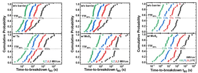
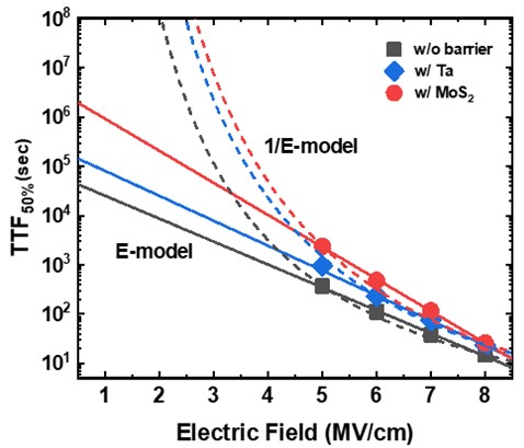
The diffusion barrier property of MoS2 was measured by Time-Dependent Dielectric Breakdown (TDDB), and evaluated by time-to-fail with a probability of 50% (TTF50%). Fig. 3. shows the cumulative distribution of tBD, with the condition of without barriers, with 3nm Ta barriers and 3nm MoS2 barrier in the capacitance structure. With the addition of the MoS2 barrier, the TTF50% was apparently enhanced from 15 to 26 s at 8 MV/cm, from 38 to 117 s at 7 MV/cm, from 111 to 482 s at 6 MV/cm, and from 373 s to 2392 s at 5 MV/cm, showing the significant improvement in device lifetime at low field. Also, compared with the same thickness of Ta barrier, the MoS2 obviously has better anti-diffuse ability.
|
(a)
|
(b)
|
(c)
|
|
|
|
|
|
Fig. 3.
|
Fig. 4.
|
The E-model and 1/E-model are often referred to as the upper bound and lower bound of the prediction range (Fig. 4). The lifetime at the normal operating field (defined at 0.5 MV/cm) was increased by 45.2x (E-model) or 1014x (1/E model) times with the MoS2 barrier. Since the general device operating temperature may be higher than 80 °C, it was necessary to confirm MoS2 barrier layer still have its lifetime advantage under high operating temperature. Here, we take TDDB measurement at constant field (6 MV/cm), varying from 25°C, 50°C, 75°C and 100°C, respectively. Fig. 3c shows the TDDB measurement under various temperatures, and it can be observed that tBD shows decreased trend with raised temperature. In spite of this trend, MoS2 still maintains excellent barrier ability. MoS2 synthesis via MW-PECVD showed the great compatibility of BEOL.; Furthermore, we measure TDDB under various electric field and temperature, the results reveal that MoS2 has great barrier layer property.
Simulation analysis of the corneal transparency and scleral opacity
Professor Snow H. Tseng's Laboratory
Graduate Institute of Photonics and Optoelectronics, National Taiwan University
Abstract: By implementing the pseudospectral time-domain (PSTD) simulations of Maxwell’s equations, we rigorously investigate the transparency and opacity of human scleral and corneal tissues. We model light propagation through realistic representations of scleral and corneal nanoarchitecture and analyze the transmittance and spatial correlation in the near field. Simulation findings reveal differences in optical transparency between these tissues due to microscopic arrangements and polydispersity of the collagen fibrils.
Transmission through various thickness of scattering media
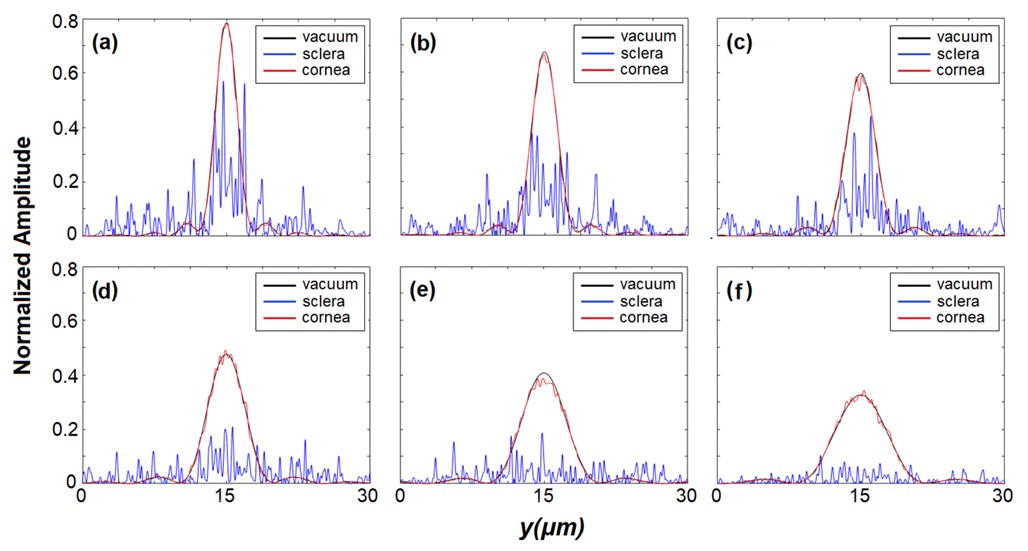
We model light propagation through scattering medium of various thicknesses in the near field. The light propagation is nearly unaltered when passing through the corneal geometry. However, light propagation in scleral geometry is severely randomized into all directions. It is evident that with increased thickness, the corneal geometry supports light penetration similar to that in vacuum, as opposed to the opacity of the scleral geometry.
|
|
|
Figure: Comparison of the transmitted light through sclera-like and cornea-like scattering media of thickness: (a) 20 μm, (b) 25 μm, (c) 35 μm, (d) 45 μm, (e) 55 μm, and (f) 65 μm. The wavelength of the incident light is 400nm. Increased sample thickness results in a progressive reduction of light transmission through the scleral medium, whereas light propagating through corneal medium is minimally affected and comparable to propagation in vacuum.
|
The Progress in the Colloidal Quantum Dot Based Color Conversion Layer
Professor Chien-chung Lin
Graduate Institute of Photonics and Optoelectronics, National Taiwan University
The progress in the past few years has put micro LED and related technologies in the roadmap for the next generation of smart displays. One of the key issues is the realization of a full-color display with a reasonable power consumption and footprint. The color conversion mechanism was often discussed in this direction and several labs around the world have demonstrated that this is feasible. There are many examples that can show great effects of color conversion: phosphors, chemical dyes, light emitting organic materials or inorganic colloidal quantum dots (CQDs). Although these materials can usually reach a conversion efficiency of 60 or 70% or even higher, the incapability of micro-pattern has become a major problem for all. In order to pattern them into an array of pixels, we have to either cast these materials accurately one by one or to mix them with photosensitive resin. Either way takes tremendous efforts to achieve good results. Among these color conversion materials, colloidal quantum dots are very promising due to their high conversion efficiency and small sizes. In our lab, we focus on two methods of these nanoparticles [1-3]: direct dispense and mixing CQD with photoresist. With the collaboration between our lab and the ITRI team, we demonstrated several different results of CQDs with micro LEDs previously [1-3].
|
|
|
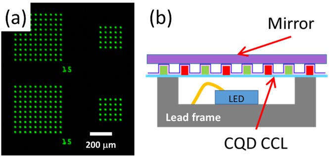
Fig. 1. (a) arrays of CQD pixels under the FLOM [4]; (b) the experimental setup [4].
|
Recently, the team from GIPO (Prof. Chung-Chih Wu and us) and from NYCU(陽明交通大學)worked together to demonstrate a semiconductor grade color conversion layer [4]. The distance between the pixels can be determined by the semiconductor grade of process which can improve the accuracy of the array greatly. The direct dispense method can ensure the highest concentration of CQDs presenting in each pixel. At the same time, we applied a reflective mirror on the top of this color conversion layer to enhance the photon recycling and a more-than-35% increase of CQD emission peak intensity was recorded. The corresponding numerical model was also developed under the incoherent reflection and transmission consideration. The result was just published in IEEE Photonics Journal and its website is: https://ieeexplore.ieee.org/abstract/document/10149805.
Reference:
[1] K.-L. Liang, W.-H. Kuo, H.-T. Shen, P.-W. Yu, Y.-H. Fang, and C.-C. Lin, "Advances in color-converted micro-LED arrays," Japanese Journal of Applied Physics, vol. 60, no. SA, p. SA0802, 2020/10/16 2020, doi: 10.35848/1347-4065/abba0f
[2] C.-C. Lin, K.-L. Liang, W.-H. Kuo, H.-T. Shen, C.-I. Wu, and Y.-H. Fang, "Colloidal Quantum Dot Enhanced Color Conversion Layer for Micro LEDs," IEICE Transactions on Electronics, vol. E105.C, no. 2, pp. 52-58, 2022, doi: 10.1587/transele.2021DII0005
[3] Y.-M. Huang et al., "The Aging Study for Fine Pitch Quantum-Dot Array on LEDs," in Conference on Lasers and Electro-Optics, San Jose, California, 2019/05/05 2019: Optical Society of America, in OSA Technical Digest, p. SF2O.2, doi: 10.1364/CLEO_SI.2019.SF2O.2
[4] G. Y. Lee et al., "Photonic Characterization and Modeling of Highly Efficient Color Conversion Layers With External Reflectors," IEEE Photonics Journal, vol. 15, no. 4, pp. 1-10, Art no. 2201110, 2023, doi: 10.1109/JPHOT.2023.3285667
|