|
Simultaneous oscillation of dual-wavelength optical parametric oscillators on monolithic c(2) nonlinear photonic crystals
Professor Lung-Han Peng
Graduate Institute of Photonics and Optoelectronics, National Taiwan University
Multi-wavelength visible laser sources are desirable to some research regimes, for example, multi-wavelength yellow orange laser can be used in stimulated emission depletion (STED) microscopy and in the colocalization analyses. However, to produce multi-wavelength visible laser through quasi-phase matched (QPM) nonlinear photonic crystals (NPCs), multi-wavelength near infrared (NIR) laser source would become a critical issue. The studies of multi-wavelength NIR optical parametric oscillators (OPOs) of aperiodic or apodized designs had been published, but the wavelength stability or tunability of such designs were not very well. The main reason is the gain competition of multi-wavelength OPOs, it would degrade the performance of multi-OPOs. To reduce the gain competition, we proposed a parallel design of multi-OPOs, i.e., the QPM periodicities were placed in transversal way of pump beam. In this way, the gain competition would be mitigated compared with the cascaded designs. In the following, the characteristics of a dual- or double-OPOs would be demonstrated, including the slope efficiency and wavelength tunability. Moreover, we will build a yellow-orange laser via sum frequency generation (SFG) or second harmonic generation (SHG) of dual-idlers of our dual-OPOs on monolithic NPC. Our design can not only facilitate simultaneous multi-wavelength oscillation in NIR band, but also had great potentials in generation of multi-wavelength lasers source in visible or even UV bands.
|
|
|
|
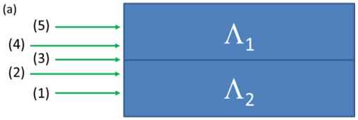
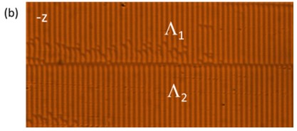
Fig. 1. (a) Design of double-OPOs, where L1= 7.67 mm, L2= 7.66 mm. The numbers of 1 to 5 designate the input pump beam position. (b) Micrograph of –z surface of periodically-poled lithium tantalate (PPLT).
|
| Position |
(1) |
(2) |
(3) |
(4) |
(5) |
| Slope efficiency (%) |
12.9 |
12.1 |
12.5 |
11.8 |
12.9 |
| Threshold (MW/cm2) |
16.2 |
26.4 |
28 |
22.8 |
13.9 |
|
Table 1. slope efficiencies and thresholds at five different input pump positions.
|
|
|
|
|
|
|
|
|
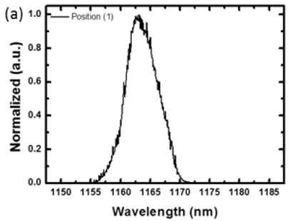
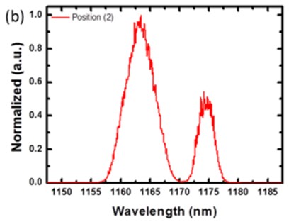
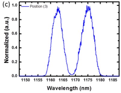
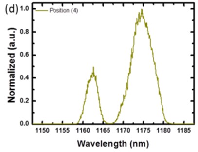
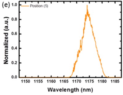
Fig. 2. (a) Idler spectrum at position (1). (b) Idler spectra at position (2). (c) Idler spectra at position (3). (d) Idler spectra at position (4). (e) Idler spectra at position (5).
|
|

|
|
Fig. 3. The design of yellow-orange laser on monolithic PPLT, here L=10.057 mm.
|
|
|
|
|
|
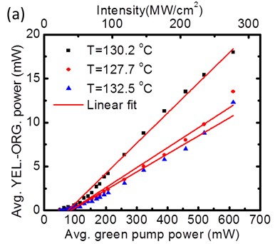
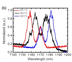
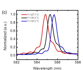
Fig. 4. (a) the slope efficiencies of yellow-orange laser at three different temperatures. Note that, at T=130.2 oC, the yellow-orange was generated by SFG, and at T=127.7 oC and 132.5 oC, it was produced by SHG. (b) The spectra of dual-idlers at three different temperatures. (c) The spectra of yellow-orange laser at three different temperatures.
|
Ultra-broadband wavelength-swept crystal fiber laser
Professor Sheng-Lung Huang
Graduate Institute of Photonics and Optoelectronics, National Taiwan University
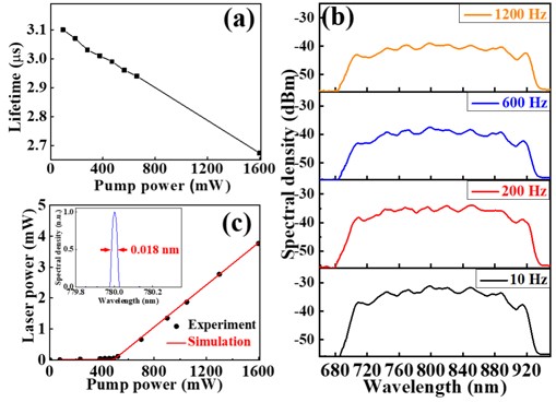
Ultra-broadband wavelength-swept laser (WSL) was generated using glass-clad Ti:sapphire crystal fiber as the gain media. With the low signal propagation loss of the crystal fiber, the swept laser has a tuning bandwidth of 250 nm (i.e., 683 nm to 933 nm) at a repetition rate of 1200 Hz. The steady-state and pulsed dynamics of the WSL were analyzed. The 0.018-nm instantaneous linewidth corresponds to a 3-dB coherence roll-off of 7 mm. When using the laser for swept-source optical coherence tomography, an estimated axial resolution of 1.8 μm can be achieved.
|
|
|
Fig. 1. (a) Fluorescence lifetimes of the Ti:sapphire CF. (b) The spectra of WSL at different repetition rates. (c) The L-I curve by two 520-nm LDs pumping. The inset shows the measured instantaneous linewidth.
|
Reference:
Y. C. Lin, T. I Yang, and S. L. Huang, “Ultra-broadband wavelength-swept Ti:sapphire crystal fiber laser,” Opt. Lett. 47, No. 11, pp. 2778–2781, 2022.
Revealing the interlayer van der Waals coupling of epitaxially-grown few layers MoS2 by terahertz coherent phonon spectroscopy
Professor Chi-Kuang Sun
Graduate Institute of Photonics and Optoelectronics, National Taiwan University
Semiconducting 2D materials such as layered-stacking MoS2 were widely considered as a versatile platform for electronics design and for novel physics research. Due to their excellent electronic and optical properties, the direct and large area synthesis method for few-layer MoS2 is in demand. However, numerous studies have reported that the van der Waals (vdWs) interfaces are commonly defective, and thus it is crucial to have a non-destructive detection technique to monitor and ensure the high interfacial quality. In this work, we employed picosecond ultrasonics technique to observe the actual interlayer vdWs bonding strength. Since the observed physical quantity is determined by the electronic behavior of the 2D structure, it serve as a good indicator for the performance of these devices.
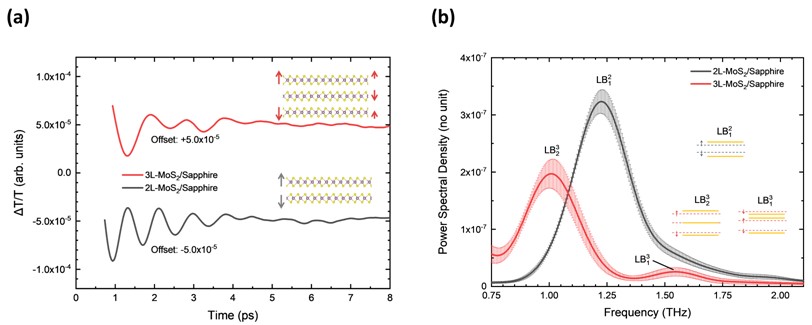
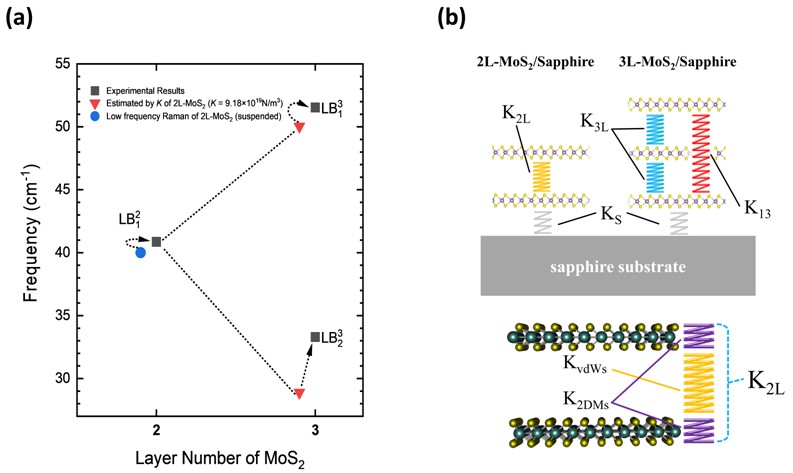
We first applied THz coherent phonon spectroscopy to optically probe the vibrational modes of the epitaxially-grown bi-layer and tri-layer MoS2. The interlayer out-of-plane vibrations beyond 1 THz were stimulated and temporally retrieved by femtosecond laser pulses (see Fig. 1(a)), revealing both Raman-active and Raman-inactive modes in one measurement (see Fig. 1 (b)). With the complete breathing modes revealed, here we extend the linear chain model by considering the elastic contact with the substrate and the vdWs coupling of next-nearest-layer to analyze the effective spring constants. We further considered the intralayer stiffness as a correction term to acquire the actual interlayer vdWs coupling. Our THz phonon spectroscopy results provide the interlayer spring constants for bi-layer and tri-layer, and a softening effect was observed when layer number decreases. The extended model further suggests that a non-negligible substrate mechanical coupling and the next-nearest-neighbor vdWs coupling have to be considered, and both of them are responsible for the correction of the large deviation when comparing with the lowest Raman active mode (see Fig. 2).
|
|
|
Fig. 1. (a) The measured interlayer-resonance-induced optical transmission change of bi-layer and tri-layer MoS2, showing a decaying negative cosinusoidal displacement of the layers; (b) Coherent phonon spectra of the bi-layer (black line) and tri-layer (red line) MoS2. Contents of this figure has been published on the Photoacoustics (2022) (see ref [1]).
|
|
|
|
Fig. 2. (a) The fan diagram of LB modes of bi-layer and tri-layer MoS2 from the experiments, cited reference for low-frequency Raman result, and the simple LCM model prediction; (b) Schematically illustrating the complete models with interlayer vdWs coupling, next nearest neighbour effect, substrate’s mechanical coupling (top), and intralayer stiffness (bottom) considered. Contents of this figure has been published on the Photoacoustics (2022) (see ref [1]).
|
Reference:
[1] P.-J. Wang, P.-C. Tsai, Z.-S. Yang, S.-Y. Lin, C.-K. Sun, "Revealing the interlayer van der Waals coupling of bi-layer and tri-layer MoS2 using terahertz coherent phonon spectroscopy," Photoacoustics 28 (2022)
Design and Analysis of Integral Imaging based 3D Light-Field Display
Professor Hoang-Yan Lin
Graduate Institute of Photonics and Optoelectronics, National Taiwan University
The integral-imaging based 3D light field display can restore its light-field information, reconstruct different images in different depth planes, and realize the floating projection effect. In the metaverse, AR/VR wearable devices, HUD for smart cockpits, medical care, entertainment, art performance and other scenarios, naked-eye 3D display is one of the most crucial requirements for the coming future.
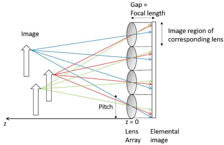
Using the Computer Generated Elemental Image (CGEI) algorithm, we realize the generation of elemental image from the 2D image and its depth map, and use the ray-tracing method to simulate and analyze the reconstructed planes of different depths. Finally, naked eye 3D display and VAC free can be achieved.
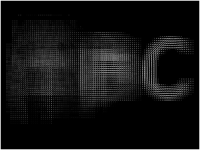
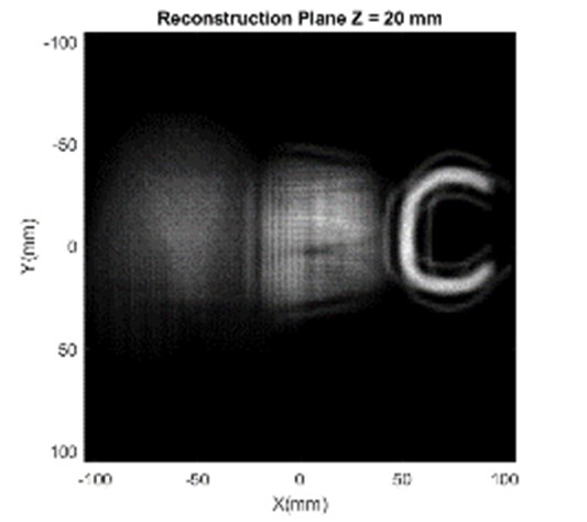
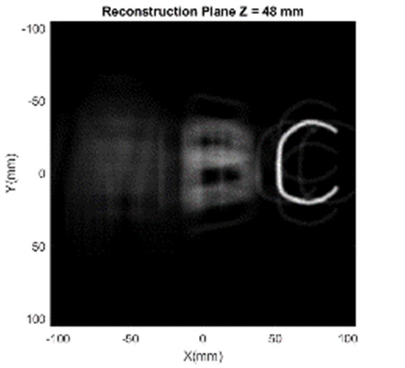
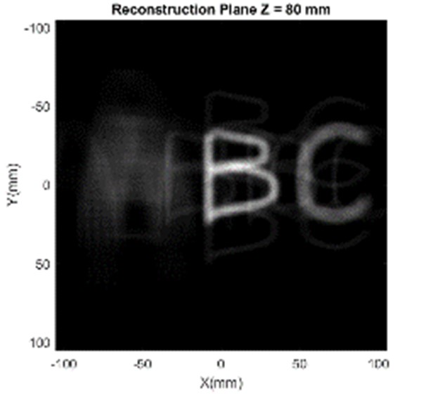
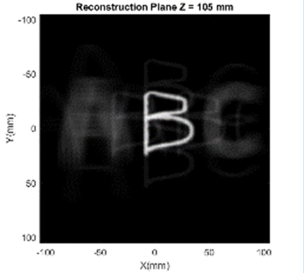
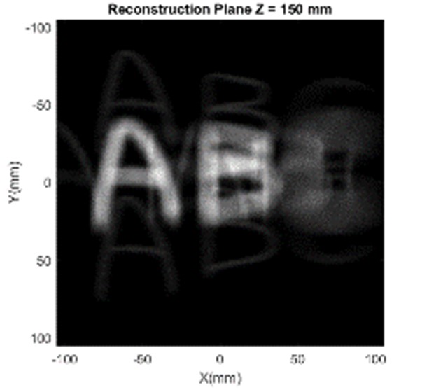
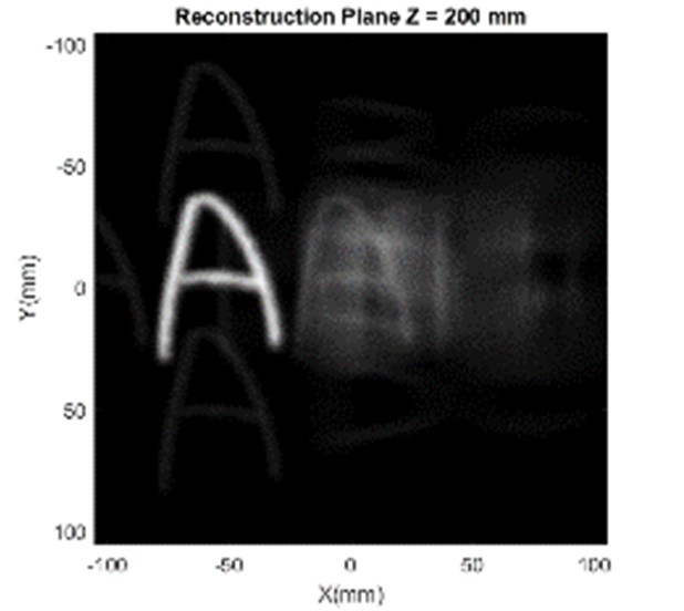
Fig. 1 shows the design principle of the CGEI algorithm. Using the reversibility of light, the floating image can be restored during the display process. We input an image of ABC, and set the depth of "A" to 200 mm, the depth of "B" to 105.37 mm, and the depth of “C” to 48 mm. Using the CGEI algorithm, the elemental image is calculated as follows in Fig. 2. Considering the real display environment, we use the Monte Carlo ray tracing method of the software LightToolsTM for simulation and analysis. We set the receiver depth to 20 mm, 48 mm (“C”), 80 mm, 105.37 mm (“B”), 150 mm, 200 mm (“A”), and the results are shown in Fig 3.
|
|
|
Fig. 1. Design principle of CGEI algorithm.
|
|
|
|
Fig. 2. Calculated elemental images.
|
|
|
|
|
|
(a) z = 20mm
|
(b) z = 48mm
|
(c) z = 80mm
|
|
|
|
|
|
(d) z = 105.37mm
|
(e) z = 150mm
|
(f) z = 200mm
|
|
Fig. 3. Images at reconstruction planes of different depths.
|
Reference:
Kai-Siang Hsu, Chia-Yuan Chang, and Hoang-Yan Lin, "Design and Analysis of Integral Imaging based 3D Light-Field Display," IDW 2022.
Photonic Inter-Layer Vias (photonic ILVs)- Three-Dimensional Inter-Layer Optical Signal Transmission Realized by a Monolithically Integrated Carrier Transport Structure
Professor Ming-Hua Mao's Laboratory
Graduate Institute of Photonics and Optoelectronics, National Taiwan University
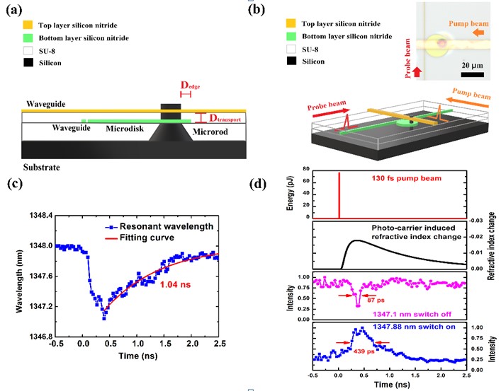
We proposed and demonstrated a brand new type of monolithic photonic devices which realizes the three-dimensional (3D) all-optical switching for inter-layer signal transmission. This device is composed of a vertical Si microrod which serves as optical absorption material within a SiN waveguide in one layer and as an index modulation structure within a SiN microdisk resonator lying in the other layer. The ambipolar photo-carrier transport property in the Si microrod was studied by measuring the resonant wavelength shifts under continuous-wave laser pumping. The ambipolar diffusion length can be extracted to be 0.88 μm. Based on the ambipolar photo-carrier transport in a Si microrod through different layers, we presented a fully-integrated all-optical switching operation using this Si microrod and a SiN microdisk with a pump-probe technique through the on-chip SiN waveguides. The switching time windows for the on-resonance operation mode and the off-resonance operation mode can be extracted to be 439 ps and 87 ps, respectively. This device shows potential applications for the future all-optical computing and communication with more practical and flexible configurations in monolithic 3D photonic integrated circuits (3D-PICs).
This work has been published in Optics Express: Yu‑Chien Wei and Ming‑Hua Mao*, "Three-Dimensional Inter-Layer Optical Signal Transmission Realized by a Monolithically Integrated Semiconductor-based Carrier Transport Structure," Optics Express, 31, 11820, (2023).
|
|
|
Figure 1. (a,b) Schematics of the device and the measurement setup. Inset in (b) is a top-view optical image of a photonic ILV device. (c) Temporal evolution of the resonant wavelength for the SiN microdisk with a vertically inserted Si microrod under femtosecond pulse excitation. (d) Switching dynamics at wavelengths of 1347.1 nm (pink curve) and 1347.88 nm (blue curve), respectively. The calculated photo-carrier induced refractive index change of a silicon microrod at the cavity layer (black curve) and the original femtosecond laser signal (red curve) are also shown.
|
|