|
The Highly-efficiency 1.55-µm DFB laser with ns-level pulsed for LiDAR applications
Professor Chao-Hsin Wu
Graduate Institute of Photonics and Optoelectronics, National Taiwan University
Our team demonstrated a highly efficient 1.55 µm distributed feedback (DFB) laser diode. The optimized epitaxial structure resulted in a low threshold current of 12 mA and a high operating efficiency of 0.433 W/A. The laser exhibited stable single mode characteristics in both high bias current and wide temperature range testing. Additionally, the ns-level pulsed operation characteristics of the DFB laser were verified, achieving a pulse peak power of 6.27 W with a pulse optical width of 20.4 ns. The watt-level pulse optical power was achieved with a single active region. With its eye-safe wavelength, high operating efficiency, stable single-mode spectral characteristics, and high pulse optical power, the 1.55 µm DFB laser is a promising light source for ToF-based LiDAR systems.
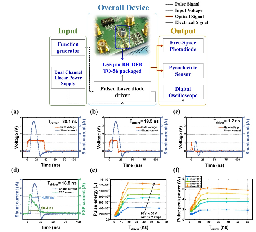
Under continuous-wave operation, the resistance is 3.17 ohm, and the optical power reaches 91 mW with a current of 0.3 A. In addition, the DFB laser displays excellent wavelength stability, maintaining an SMSR of over 33 dB even at high temperatures, thus ensuring stable single longitudinal mode operation. Then we estimate the pulse operation of the DFB laser using the narrow pulse generator. When Vbus is 50 V and Tdriver (pulse generator) is 18.5 ns, the experimental results show the time widths of the shunt current and optical signal are 14.58 and 20.4 ns, respectively. The pulse energy received by the pyroelectric sensor is 128 nJ, and the pulse peak power reaches up to 6.27 W.
This work has been published in Optics Letters: Te-Hua Liu, Hao-Tien Cheng, Jau-Yang Wu, and Chao-Hsin Wu*, "Achieving ns-level pulsed operation of up to 6.27 W with a 1.55-µm BH-DFB laser for LiDAR applications," Opt. Lett. 48, 3071-3074 (2023)
|
|
|
Fig. 1. (upper) Experimental configuration for ns-level short-pulse operation. (lower) (a) Electrical signal of the driver when Tdriver is 38.1 ns. (b) Electrical signal of the driver when Tdriver is 18.5 ns. (c) Electrical signal of the driver when Tdriver is 1.2 ns. (d) The oscilloscope monitors the shunt current and the optical signal of the FSP when Tdriver is set as 18.5 ns. (e) Comparison of the pulse energy received by the pyroelectric sensor under a range of Vbus and Tdriver parameters. (f) Comparison of the pulse peak power of the pulsed laser driver with the pulse width under different Vbus.
|
Development of an automatic analysis algorithm for the quantitative assessment of the human skin with a portable optical coherence tomography system
Professor Hsiang-Chieh Lee
Graduate Institute of Photonics and Optoelectronics, National Taiwan University
Optical coherence tomography (OCT) enables noninvasive, real-time, and volumetric imaging of skin architectures. In this study, we collected skin OCT images from different human body sites of 25 subjects with a prototype, portable spectral-domain OCT system. The contrast of the OCT images was effectively adjusted through optical attenuation coefficient (OAC) computation. This enables the development of a fully automatic segmentation algorithm, providing the parameters including the (i) epidermis thickness and the (ii, iii) roughness of the boundary between epidermis and air as well as epidermis and dermis. Also, the (iv, v) OAC values of the epidermis and upper dermis layer are available. This study demonstrated the quantitative assessment of the human skin with five different metrics aforementioned, which might benefit the implementation of skin OCT imaging in the field of Cosmetology or Aesthetic Medicine.
|
|
|
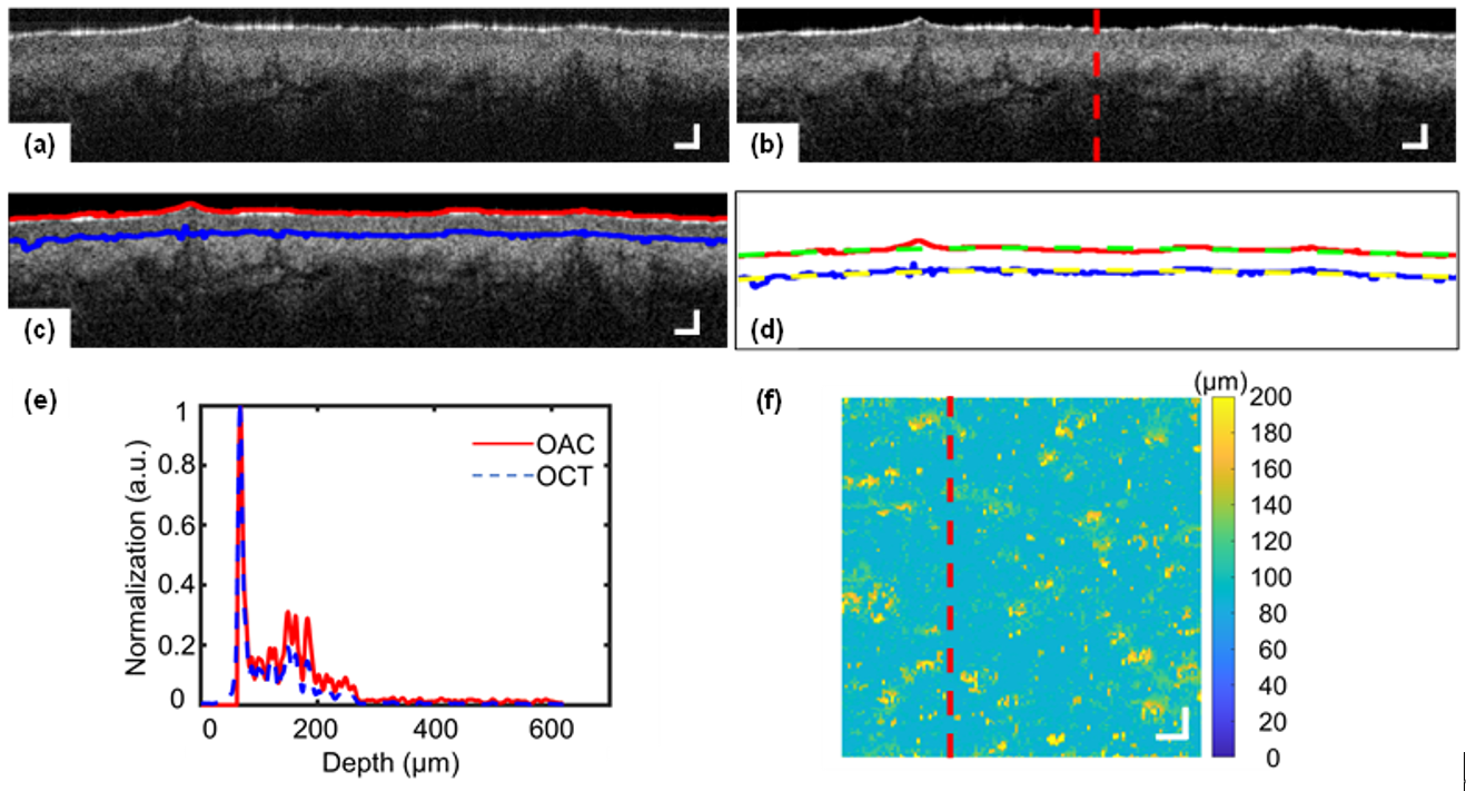
Fig. 1. Segmentation of skin epidermis using gradient variation rate of optical attenuation coefficient (OAC) (a) Cross-sectional OCT image of left cheek skin of a 32-year-old male. (b-c) Cross-sectional OAC image of (a). The region between the red and blue lines in (c) shows the layer of the epidermis. The green and blue lines in (d) show 3rd-degree polynomial curve fitting lines corresponding to the red and blue lines in (c), respectively. (e) Normalization of OCT and OAC signals from the position of the red dash line in (b), where the OAC signal could enhance the OCT signal. (f) En-face image from the 3D volumetric OAC image indicates the depth distribution, where the red dash line indicates the position of (a). Scale bars of (a-c) and (f) are 100 and 250 μm, respectively.
|
Efficiency Enhancement of Photon Color Conversion from an InGaN/GaN Quantum Well into a Colloidal Quantum Dot Located in a Metal Nanotube
Professor C. C. Yang's Laboratory
Graduate Institute of Photonics and Optoelectronics, National Taiwan University
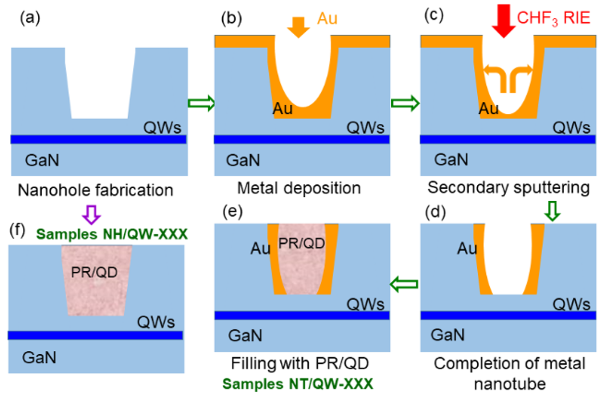
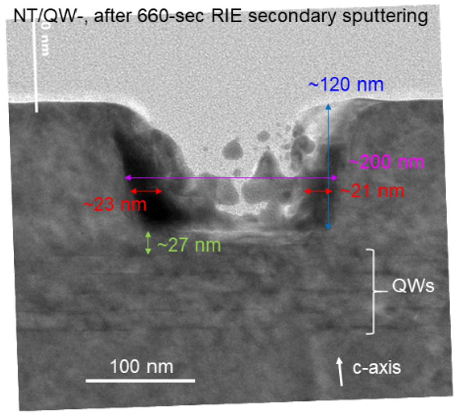
For implementing a surface plasmon (SP) coupling effect to enhance the efficiency of the color conversion from a blue-emitting InGaN/GaN quantum well (QW) into green- and red-emitting colloidal quantum dots (QDs), an Au sidewall layer is fabricated in a surface nanohole (NH) on a QW template to form an Au nanotube (NT) structure for accommodating the inserted QDs. The Au sidewall layer is implemented through Au deposition, followed by a secondary sputtering process in a reactive ion etching chamber. The enhanced efficiency of the Förster resonance energy transfer (FRET) from the underlying QW structure into the inserted QDs is observed, when compared with the result of a surface NH sample without Au sidewall layer. Meanwhile, with a QD inserted into an Au NT, its emission efficiency is increased, when compared to that of a QD inserted into a GaN surface NH. Those efficiency increases are caused by the SP coupling effect of the Au sidewall layer. The combined effect of the efficiency increases of FRET and QD emission leads to an enhanced color conversion process. Figures 1(a)-1(e) show the procedures for fabricating a metal nanotube (NT/QW-XXX) sample. Figure 1(f) shows the structure of a nanohole (NH/QW-XXX) sample. Figure 2 shows the TEM image of an NT/QW-XXX sample after the RIE secondary sputtering process. Here, the dark regions inside the NH correspond to the Au distribution. Table 1 shows the data of PL decay time, IQE, and FRET efficiency in various NT/QW-XXX samples, including the insertions of green QD (GQD), red QD (RQD), GQD plus RQD (GQD+RQD), and pure photoresist (PR).
|
|
|
|
Fig. 1. (a)-(e): Schematic illustrations of the procedures for fabricating an NT/QW-XXX sample. (f): Schematic illustration of the structure of an NH/QW-XXX sample.
|
Fig. 2. Cross-sectional TEM image of an NT/QW-XXX sample after the RIE secondary sputtering process.
|
|

|
|
Table 1. PL decay times of QW, GQD, and RQD emissions in those NT samples with Au sidewall layers fabricated on the QW template. The numbers inside the parentheses (curly brackets) show the QW IQEs at different fabrication stages (the FRET efficiencies from QW into QD).
|
Quasi-van der Waals epitaxy of Bi on (111) Si
Professor Hao-Hsiung Lin's Laboratory
Graduate Institute of Photonics and Optoelectronics, National Taiwan University
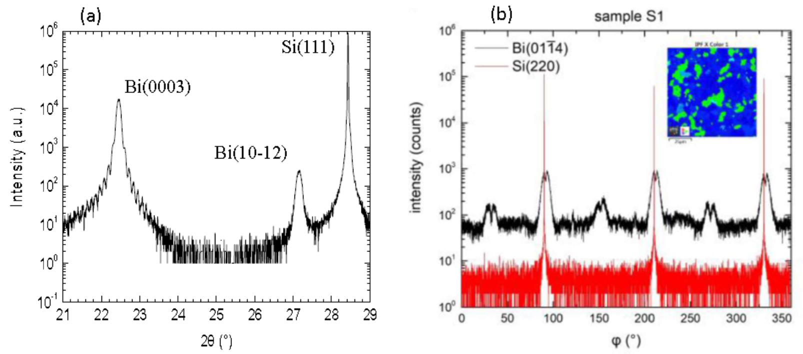
Bi is a nontrivial semimetal, with tiny negative bulk band gap and very small effective mass in certain orientations, allowing the band structure be transferred to semiconductor through quantum size effect. Because of the strong spin-orbit interaction, its surface states split into two bands with a gap of 0.8 eV, which makes it also a promising material for spintronics. In this work, Bi thin films were grown on (111) Si using MBE, and characterized using XRD, TEM, and EBSD. All the Bi films are highly (0003) textured and contain two twinning domains. The basic lattice parameters c and
a
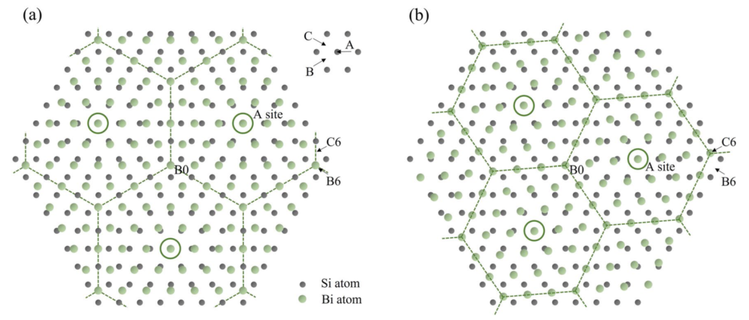
as well as b, the bilayer thickness, determined from XRD for an 80-nm-thick Bi layer, are all within 0.1% as compared with those of bulk Bi, suggesting that the Bi film is nearly fully relaxed. The rapid relaxation despite the huge 18% lattice mismatch is attributed to the quasi-van der Waals bonding at the Bi/Si interface. From the XRD φ-scans of asymmetric Bi (01-14) planes and Si (220) plane, we confirmed the well registration between the lattices of Si and Bi lattice. For the ~10-nm-thick layers, a strain ~2% is observed. From (01-14) φ-scan, we observed an additional rotation phase. We proposed a preferential closed-pack A-B-C site model to explain the observed rotation phases.
|
|
|
Fig. 1. (a) Ω-2θ scan showing the nearly fully relaxed (0003) Bi phase. (b) A (01-14) ϕ-scan showing the dual-peak twinning Bi phases. One of the phases aligns the (220) of Si substrate. EBSD inverse pole figure shown in the inset, green and blue represent the regions of the two twinning phases.
|
|
|
|
Fig. 2. Two Bi atomic arrangements based on preferential site model. (a) Bi hexagonal lattice aligns Si lattice with 6aBi = 7aSi and (b) Arrangement for the rotation phase with tilted Bi hexagonal lattice and 6aBi = 7.024 aSi. The preferential sites in both figures form superlattice indicated by dashed hexagons.
|
|