|
30 GHz Highly Damped Oxide Confined Vertical-Cavity Surface-Emitting Laser
Professor Chao-Hsin Wu
Graduate Institute of Photonics and Optoelectronics, National Taiwan University
Oxide-confined 850-nm vertical-cavity surface-emitting lasers (VCSELs) are reliable light sources for short-reach multi-mode optical communication applications due to their high efficiency, ease of fabrication, reliability, and small foot-print. 850 nm VCSELs with non-return-to-zero (NRZ) and 4-level pulse amplitude modulation (PAM-4) modulation have provided backbone optical interconnects for 400 and 800 Gigabit Ethernet networking technologies. The dramatically increasing data demand drives the VCSEL-based multi-mode fiber (MMF) links to equip advanced modulation schemes such as PAM-4, which puts specific emphasis on the dynamics performance of VCSELs, such as high bandwidth at low current, sharp edge in S21 response, and low intrinsic noise. Various methods have been investigated to reduce the device parasitics, increase modulation bandwidth and yield highly damped modulation responses.
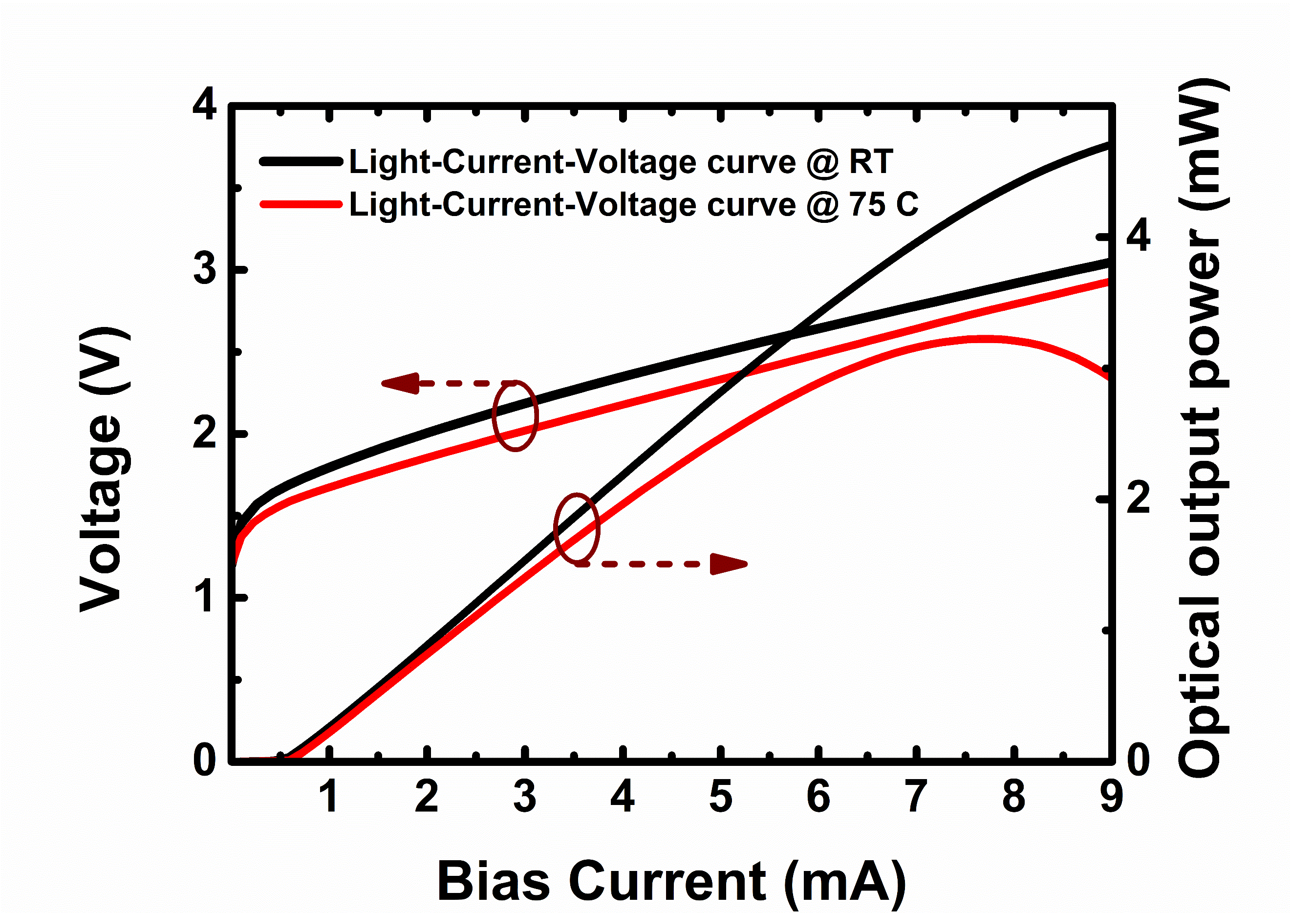
Our device employs six-pairs thick oxide aperture for a reduced device parasitics capacitance and an optimized relaxation oscillation damping with currents for high quality eyes at the targeted data rates. The highly-damped VCSEL exhibits a low thermal impedance, ultra-high bandwidth, and delivers a flat modulation response. The L-I-V curve of our high damped VCSEL with 3.5 μm oxide aperture at room temperature (RT) and 75°C is shown in Fig. 1. The VCSEL exhibit a peak optical power of 3.88 mW and roll-over current over 9 mA. Fig. 2 shows the measured modulation responses and the VCSEL exhibits flat modulation responses at various biases at RT and 75°C. When biased at 5 mA, the VCSEL reached 27.3 GHz and 25.2 GHz at RT and 75°C respectively, and showed a mere 2.1 GHz decrease in modulation bandwidth at the elevated temperature. The fitted MCEF is 12.2 GHz / mA1/2 and is illustrated in Fig. 3. We have demonstrated an ultra-fast highly damped VCSEL with a flat modulation response for up to 30 GHz. We employed several optimizations in the design of the VCSEL, including the intrinsic dynamic performance, RC parasitics, and photon lifetime tuning, which enable a thermally-stable operation for up to 75°C. The flat modulation characteristics of the VCSEL could enable over 100 Gb/s line rates PAM-4 modulation for 400G and 800G high-capacity optical interconnect systems.
|
|
|
Fig. 1. The L-I-V characteristics for a ~3.5 μm oxide aperture diameter at RT and 75°C.
|
|

|
|
Fig. 2. The S21 optical response when 3 mA, 5 mA, and 7 mA at RT and 75°C.
|
|

|
|
Fig. 3. 3 dB bandwidth plotted against square root of biased current and MCEF fits.
|
Step-shaped electrode for Blue Phase transflective liquid crystal displays
Professor Wing-Kit Choi
Graduate Institute of Photonics and Optoelectronics, National Taiwan University
In recent years, our laboratory has been proposing new electrode designs for blue phase liquid crystal displays (LCDs) with high light efficiency and low operation voltage. One such design is shown in figure 1 below for a transflective LCD. We named this design “step-shaped electrode”. By using this design, it is possible to produce a blue-phase transflective LCD with very high light efficiency of > ~ 95% at low operation voltage of ~ 9 to 13V with well-matched T-V and R-V electro-optic curves as shown in figure 2. This design is based on the concept of forming fairly strong and uniform horizontal electric fields above the reflective (R) region which has a step-shaped reflective electrode and also above transmissive (T) region which is enhanced by the vertical wall-like electrode. These strong electric fields help minimize the dead-zones which normally exist above electrodes (as illustrated in figure 3) and hence enhance the transmission/reflection and lower the operation voltage.
|

|
|
Figure 1. Structure of a blue-phase transflective LCD with step-shaped electrodes
|
|

|
|
Figure 2. Normalized transmission (T) and reflection (R) of step-shaped electrode blue-phase transflective LCD with two matched designs A and B
|
|

|
|
Figure 3. Top-view transmission (T) and reflection (R) profiles of a step-shaped electrode blue-phase transflective LCD showing almost no dead zone exist above electrodes
|
High-speed optical coherence tomography imaging with a MEMS-tunable HCG-VCSEL light source
Professor Hsiang-Chieh Lee
Graduate Institute of Photonics and Optoelectronics, National Taiwan University
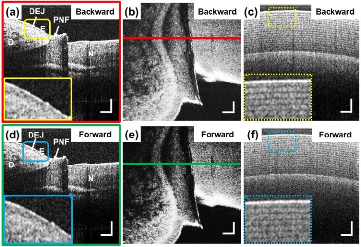
We present a high-speed swept-source optical coherence tomography (SS-OCT) imaging system using an electrically-pumped, micro-electromechanical (MEMS)-tunable high-contrast grating (HCG) VCSEL light source. The developed SS-OCT system exhibits an A-scan rate of 250 kHz, which can be further improved to 500 kHz if both the backward and forward laser sweeps are used. Comparing to existing MEMS-tunable VCSEL light sources, the use of HCG structure as the top reflection mirror for the VCSEL cavity not only simplifies the manufacturing process but also better keeps the light polarization state during the wavelength sweeping. In the experimental setup, a dual-channel acquisition scheme was utilized to provide calibration of the OCT signal with a separate calibration interferometer. Volumetric imaging of the human fingernail junction and mouse ear skin in vivo shows the feasibility of providing high speed imaging of the tissue architectures. In addition, utilizing the OCT angiography (OCTA) in combination with the variable interscan time analysis (VISTA) algorithm, it could provide subsurface volumetric microvascular imaging of the mouse ear skin with relative blood flow speed information. The electrically-pumped, MEMS-tunable HCG-VCSEL light source can provide high-speed OCT and OCTA imaging with a more compact light source footprint and potentially a lower cost.
|
|
|
Fig. 1. Cross-sectional and en face OCT images of the fingernail junction using the OCT data corresponding to the (a, b) backward and (d, e) forward sweeps, respectively. (e, f) Cross-sectional OCT images of a roll of Scotch tapes using the OCT data for the backward and forward sweeps, respectively. Insets (a, d) and (e, f): enlarged view of the region of interest indicating the epidermis observed in (a, d) as well as layer of tapes identified in (e, f), respectively. D: dermis, DEJ: dermis and epidermis junction, E: epidermis, PNF: proximal nail folder. Scale bars: 500 μm.
|
The advances of semiconductor based micro LEDs
Professor Chien-Chung Lin
Graduate Institute of Photonics and Optoelectronics, National Taiwan University
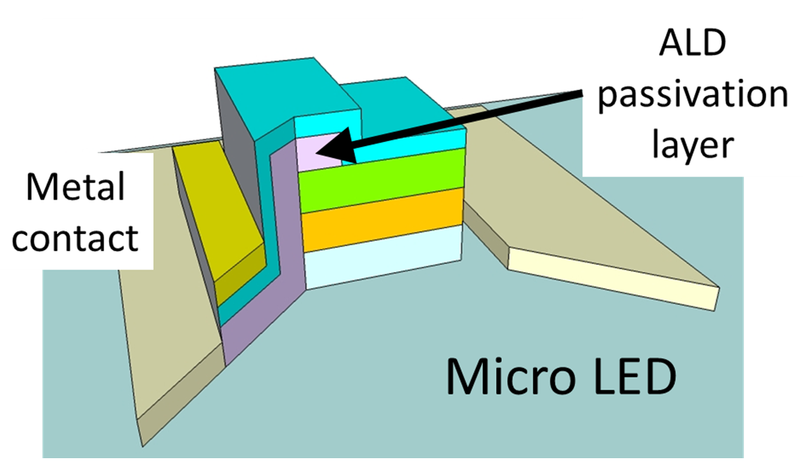
The growth of Internet traffic facilitates our daily life. From e-commerce, online game, to online video, our daily activities are full of interactions with Internet and an information based display (or a smart display) will be an important component in this scenario. In our lab, we focus our efforts on one of the important topics of this next generation displays: semiconductor based micro LEDs. Two important material systems are used for red, green, and blue color generations: Gallium nitride based (InGaN, AlGaN, GaN), and AlGaInP based materials (a finished device is shown in Fig. 1). The benefit to use semiconductor as the main host of technology is its mature fabrication and highly efficient light-emitting capability. In our lab, we demonstrated devices as small as 2 micrometers in size and emission wavelengths from ultra-violet to red can be realized[1-3]. However, to achieve high resolution in a display, we need to reduce the size of each pixel, whose sizes are determined by each LED of different colors. Another important issue that needs to be addressed is that the reduction of light emitting efficiency (or called external quantum efficiency, EQE) is inevitable when we reduce the size of the devices. This is because of the increase of the sidewall leakage and non-radiative recombination inside the devices[1-4]. To alleviate this problem, an atomic layer deposition system was used to passivation the sidewalls of the devices, as shown in Fig. 2. This passivation can effectively reduce the leakage current and boost up the illumination efficiency of the devices. The light field angular intensity is also an interesting topic for these devices[5]. Because each color has its own far field pattern, as shown in Fig. 3, the overall result needs to be investigated and modified to improve the angular uniformity of the colors in a micro-LED based display such that you will not see angle-dependent color variation. We can use chip design to compensate this variation and to achieve better uniformity.
|

|
|
Fig. 1. A 10-micron micro LED under microscope
|
|
|
|
Fig. 2. A schematic diagram of a micro LED device with ALD protection[3]
|
|

|
|
Fig. 3. Color variation due to far field pattern difference
|
[1] Y. L. Tsai et al., "Extended Electrical and Photonic Characterization of GaN-Based Ultra-Violet MicroLEDs With an ITO Emission Window Layer," IEEE Photonics Journal, vol. 12, no. 6, pages 1~9 (2020)
, doi: 10.1109/JPHOT.2020.3037220
[2] Y. Y. Li et al., "Analysis of Size-Dependent Quantum Efficiency in AlGaInP Micro–Light-Emitting Diodes With Consideration for Current Leakage," IEEE Photonics Journal, vol. 14, no. 1, pages 1~7 (2020)
, doi: 10.1109/JPHOT.2021.3138946
[3] T.-Y. Lee et al., "Increase in the efficiency of III-nitride micro LEDs by atomic layer deposition," Optics Express, vol. 30, no. 11, pages 18552~18561 (2022)
, doi: 10.1364/OE.455726
[4] H.-H. Huang et al., "Investigation on reliability of red micro-light emitting diodes with atomic layer deposition passivation layers," Optics Express, vol. 28, no. 25, pages 38184~38195 (2020)
, doi: 10.1364/OE.411591
[5] S.-M. Yang et al., "Angular color variation in micron-scale light-emitting diode arrays," Optics Express, vol. 27, no. 16, pages A1308~A1323 (2019), doi: 10.1364/OE.27.0A1308
|