|
|
 |
|
 |
| |
Publisher: Chairman Yuh-Renn Wu Editors: Professor Snow
H. Tseng, Ms. Hsiao-wen Lin September 30, 2022 |
| |
|
 |
|
Congratulations to Prof. Ching-Fuh Lin and his startup company Nano & Micro for the honor of achieving Top 10 in "2022 Taiwan Startup World Cup."
This competition is a joint effort by Taiwan ITRI New Venture Association and Pegasus Tech Venture. Out of the 175 participating teams, Prof. Ching-Fuh Lin's team made it into the Top 10.
Link: https://sites.google.com/view/swtc2022/home
Congratulations to Prof. Gong-Ru Lin and Prof. Chao-Hsin Wu for the successful publication of their research results and the honorary media coverage, in collaboration with National Yang Ming Chiao Tung University and Hong Hai Research Institute Semiconductor Division and Corning.
Link: https://www.ledinside.com.tw/news/20220516-37978.html
Congratulations to Chih-Yuan Tsai, Han-Yu Tsai, and their advisor Prof. Ching-Fuh Lin for the honor of receiving the "ISME Best Thesis Award."
Congratulations to Lu-Ching Hsueh
and his advisor Prof. Chao-Hsin Wu for the honor of receiving the "SNDCT Distinguished Thesis Award."
Congratulations to the following students for participating in International Display Manufacturing Conference 2022 and achieving the following commendations:
|
Student |
Award |
Advisor |
Shih-Min Chen
(Master Student) |
Best Paper Award - Oral
Thesis Title: Numerical Analysis for V-Shape Defect and Random Alloy Fluctuation in Red Green and Blue Nitride Based LEDs |
Prof. Yuh-Renn Wu |
Hsiao-Chun Hung
(Master Student) |
Best Paper Award - Oral
Thesis Title: A Complete Exciton Diffusion Model Including Both Singlet and Triplet Behaviors Coupling with Poisson and Drift-Diffusion Solver |
Prof. Yuh-Renn Wu |
Pu-Yuan Lin
(Master Student) |
Distinguished Poster Award - Poster
Thesis Title: Flexible Differential Amplifier Based on a-IGZO TFTs |
Prof. I-Chun Cheng |
Chieh-An Chen
(Master Student) |
Distinguished Poster Award - Poster
Thesis Title: High-Efficiency Blue Fluorescent OLED Based on Pyrene Derivative Host Material |
Prof. Jiun-Haw Lee |
Hao-Che Kao
(PhD Student) |
Distinguished Poster Award - Poster
Thesis Title: Realizing Deep-Red/Near-Infrared Phosphorescent OLED with Iridium(III) Complexes with [-2, -1, 0] Charged Ligands |
Prof. Chung-Chih Wu |
Ching-Hsiang Huang
(Master Student) |
Distinguished Poster Award - Poster
Thesis Title: High-Efficiency Deep-Blue/Ultraviolet Organic Light Emitting Diodes |
Prof. Jiun-Haw Lee |
Congratulations to Yu-Chieh Chang and Huan-Ting Shen, and their advisor Prof. Yuh-Renn Wu, for attaining the "IWUMD 2022 Best Poster Paper Award."
Congratulations to Prof. Ching-Fuh Lin for attaining the "PARC Appreciation Award."
The Palo Alto Research Center (PARC) is a research organization founded in 1970 and located in Palo Alto, CA, USA. Formerly known as Xerox PARC, the PARC is an important research center of Xerox, officially splitting off from Xerox and became a subsidiary company of Xerox in April 2002.
|
|
 |
|
 |
|
| |
|
|
|
March “GIPO Colloquium” Highlights |
|
Time: |
2:20 pm, March 11 (Fri.), 2022
|
|
Speaker: |
Li-Ya Ko (CEO, Enli Technology) |
|
Topic:
|
The making of a metrology instrument brand name and development of international standards |
| |
|
 |
|
Li-Ya Ko (Right) and Prof. Hsiang-Chieh Lee (Left) |
|
|
Time: |
2:20 pm, March 18 (Fri.), 2022
|
|
Speaker: |
Prof. Chao-Chang Chen
(Department of Mechanical Engineering, National Taiwan University of Technology) |
|
Topic: |
Applications of three dimensional IC and TSV measurement |
|
|
|
 |
|
Prof. Chao-Chang Chen (Right) and Prof. Hsiang-Chieh Lee (Left) |
|
|
Time: |
2:20 pm, March 25 (Fri.), 2022
|
|
Speaker: |
Frank F. Y. Hsu (Manager, Metrology Center, Advanced Packaging, TSMC) |
|
Topic:
|
Trends in advanced semiconductor packaging inspection
|
| |
|
 |
|
Frank Hsu (Right) and Prof. Hsiang-Chieh Lee (Left) |
|
|
April “GIPO Colloquium” Highlights |
|
Time: |
2:20 pm, April 8 (Fri.), 2022
|
|
Speaker: |
Dr. Min-Hsiu Hsieh (Quantum Computation Division, Hon-Hai Research Institute) |
|
Topic:
|
Introduction to Hon Hai Research Institute and Quantum Machine Learning
|
| |
|
|
Time: |
2:20 pm, April 15 (Fri.), 2022
|
|
Speaker: |
Dr. Wei-Che Chang (Manager, Chroma ATE) |
|
Topic:
|
Application of white light interferometer in industrial inspection
|
| |
|
|
Time: |
2:20 pm, April 22 (Fri.), 2022
|
|
Speaker: |
Rooney Tsai (Garmin) |
|
Topic:
|
From physical display to AR projection
|
| |
|
 |
|
Rooney Tsai (Right) and Prof. Hsiang-Chieh Lee (Left) |
|
|
Time: |
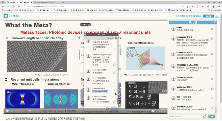
2:20 pm, April 29 (Fri.), 2022
|
|
Speaker: |
Prof. Ming-Lun Tseng (Institute of Electronics, National Yang Ming Chiao Tung Univeristy) |
|
Topic:
|
Nanophotonic Metasurfaces for UV light generation, Imaging, and Sensin
|
| |
|
|
May “GIPO Colloquium” Highlights |
|
Time: |
2:20 pm, May 6 (Fri.), 2022
|
|
Speaker: |
Dr. Ellis Chang (Co-Founder, Classical Innovation Workshop) |
|
Topic:
|
Freshmen's Keen Edge
|
| |
|
|
|
|
|
|
| |
|
|
|
Wide Field-of-View 3D MEMS LiDAR
Professor Guo-Dung Su
Graduate Institute of Photonics and
Optoelectronics, National Taiwan University
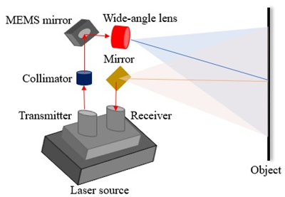
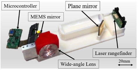
Light detection and ranging (LiDAR) sensors are promising for automated transportation to detect the surrounding environment. However, most LiDAR solutions are complex and bulky. By designing a MEMS-mirror-based LiDAR, we can improve the volume constraints, but MEMS mirrors could limit scanning angles. In this newsletter, we show and demonstrate a MEMS LiDAR system to solve the current obstacles. Combining a MEMS mirror and a wide-angle lens into the system, small-volume and large field-of-view (FOV) LiDAR systems can be realized. We use ray tracing optical simulation software to design a pair of aspherical lenses to expand the scanning angle. After the laser beam passes through the wide-angle lens, the FOV can be increased to 104 degrees. The distortion of the wide-angle lens is controlled below 3%, making the scanned image precise to the actual situation. In order to experimentally demonstrate the small-volume MEMS scanning LiDAR, a modular laser rangefinder is used with a MEMS mirror. The entire system of the LiDAR scanner is around 15 cm × 5 cm × 2.5 cm. In the natural light environment for wide-angle LiDAR measurement, the maximum error is less than 2%. Finally, an image processing program is written to convert the scanned data into a 3D point cloud image, and the generated image proves the complete function of the proposed LiDAR.
|
 |
 |
|
Fig. 1 |
Fig. 2 |
Singlet fission and triplet fusion in amorphous rubrene thin film
Professor Jiun-Haw Lee
Graduate Institute of Photonics and Optoelectronics, National Taiwan University
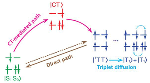
Exciton dynamics in amorphous rubrene thin film (100 nm) was investigated by steady and transient photoluminescence measurement. Upon photoexcitation, singlet exciton in rubrene thin film may give light in ~ns range which results in prompt fluorescence in transient measurement. Not only radiative recombination, singlet may also split into the triplets though singlet fission process, and two triplets may fuse back to singlet through triplet fusion process and emit light, which results in delayed fluorescence. Through spectroscopic study, at least three emitting species in this amorphous film were identified with distinct singlet fission, triplet fusion, and triplet hopping rates. It was found that singlet fission and triplet fusion both have direct path. However, singlet fission process could be mediated by charge-transfer (CT)-state which was absent in triplet fusion process.
|
|
|
Fig. 1. Energy transfer routes among singlet, triplet, and CT states. |
Study of Current Collapse Behaviors of Dual-gate AlGaN/GaN HEMTs on Si
Professor
Jian-Jang Huang’s Laboratory
Graduate Institute of
Photonics and
Optoelectronics,
National Taiwan
University
Surface traps on GaN-based HEMTs (high-electron-mobility transistors) usually
result in the increase of channel on-resistance. It becomes worsen when short
pulses are applied during high-frequency and high voltage switching. Here we
present a dual-gate transistor structure to suppress the dynamic on-resistance
increase. The auxiliary gate under a proper fixed voltage is able to induce
additional electrons to compensate the channel carrier loss during main gate
switching, leading to a lower dynamic on-resistance.
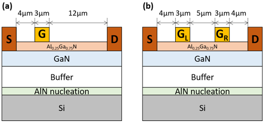
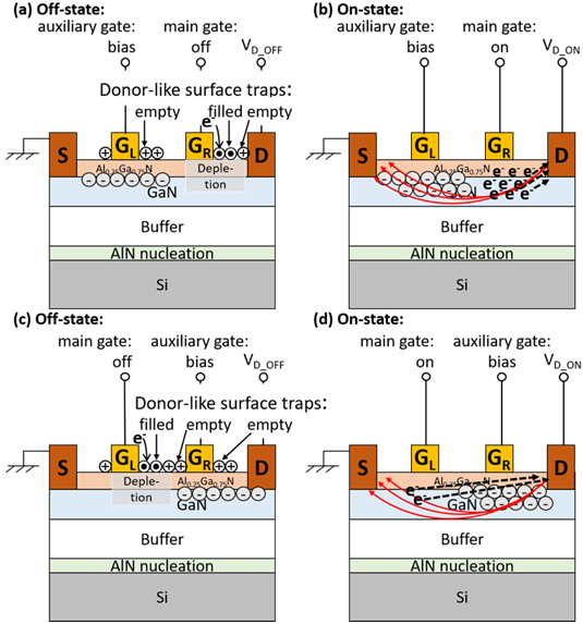
The dual-gate (DG) AlGaN/GaN HEMT is schematically shown in Fig. 1, along with a conventional device for comparisons. The DC electrical properties reveal that the drain current level of the DG-HEMT with GL-drive (main gate) and GR-float (auxiliary gate) is slightly higher than that of SG (single gate) -HEMT due to the additional carriers induced by the floating gate. The DG-HEMT with GR-drive and GL-float has the smallest current because of the largest gate-source resistance. When a bias voltage is applied on the auxiliary gate, the current level can be adjusted by the additional carriers. Since the auxiliary gate provides an extra source of supplying electrons to the channel that suffers from current collapse, we further studied current collapse phenomenon of the devices by a pulsed stress-measurement approach. The results suggest within the range of auxiliary gate bias, -2 ~ 2 V, a DG device with the main gate drive on GR and the auxiliary gate voltage of 0 V on GL has the lowest RON, while SG-HEMT is the worst in most of the stress conditions (see Fig. 2 for various drain and gate lag stresses). The improvement using the dual-gate structure is elucidated from the carrier distribution in the channel region as illustrated in Fig. 3. For the case main gate bias applied on GR and auxiliary bias on GL, the depleted carriers from the main gate can be quickly supplied by the carrier underneath the auxiliary electrode under a positive drain voltage with a slight negative impact of carriers recombined with traps on both sides of main gate. Finally, we conclude an auxiliary gate biased at 0 V near the source side results in the best suppress of current collapse.
|
 |
|
Fig. 1. Cross-sectional epi-structure of (a) a SG-HEMT and (b) a DG-HEMT. |
|
 |
|
Fig. 2. (a) Comparison of the normalized RON at various drain stress voltages, VD_OFF, and auxiliary gate biases.
|
|
 |
|
Fig. 2. (b) Comparison of the normalized RON at various gate lag stress conditions. |
|
 |
|
Fig. 3. Distribution of electrons in the channel under various biases on the main gate and auxiliary gate electrodes. GR-drive/GL-bias at (a) off-state and (b) on-state. GL-drive/GR-bias at (c) off-state and (d) on-state. Note there may be small amount of donor-like surface traps (not shown) on both sides of GL and GR, depending on the bias voltage of the auxiliary gate. |
Mobility Enhancement in P-Type SnO Thin-Film Transistors via Ni Incorporation by Co-Sputtering
Professor I-Chun Cheng
Graduate Institute of
Photonics and
Optoelectronics, National
Taiwan University
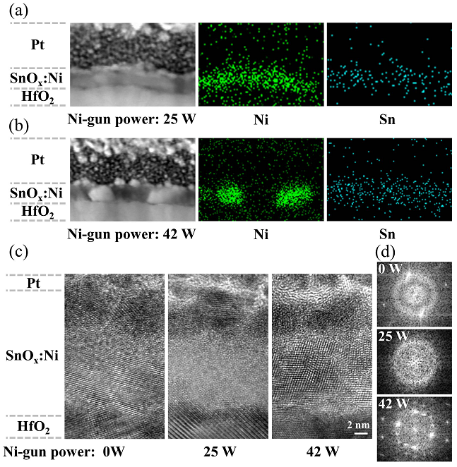
Oxide semiconductors have been considered one of the most promising candidates for flexible electronics applications owing to their low process temperatures and good reliability. However, the low mobility of p-type oxide semiconductors limits the performance of flexible oxide-TFT-based CMOS technology. In this study, p-type SnOx:Ni thin films were deposited by reactive rf magnetron co-sputtering, a technique compatible with the current industrial semiconductor manufacturing technology, from Sn and Ni targets. As the Ni-gun power increased, the distribution of Ni in the SnOx:Ni thin film changed from a more uniform dispersion to nanoclusters, resulting in the crystalline phase transition of SnOx:Ni from
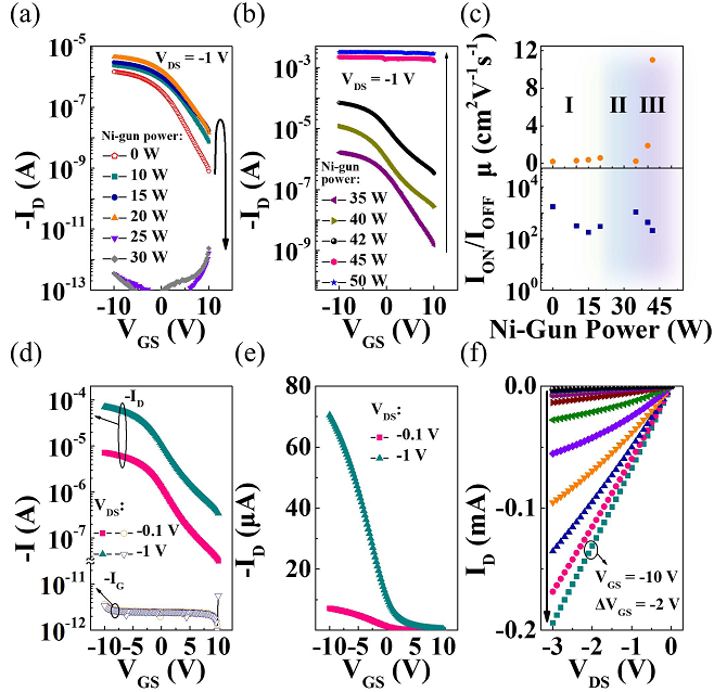
α-SnO (110)-dominant polycrystalline to amorphous and then to α-SnO (101)-dominant polycrystalline. A high-mobility inverted-staggered p-type SnOx:Ni TFT was then fabricated on a glass substrate with a maximum process temperature of 225°C, which is compatible with flexible polymeric substrates. The TFT fabricated at an optimal Ni-gun power of 42 W exhibited an impressive field-effect mobility of 11 cm2V−1s−1 and on current of 35.2 μA per channel width-to-length ratio; these values are comparable to those of a typical n-type oxide TFT. These results should contribute toward flexible oxide-TFT-based CMOS technology. [IEEE Electron Device Letters, vol. 43, No. 2, pp. 228-231, Feb 2022]
|
 |
|
Fig. 1. Elemental EDS maps of SnOx:Ni thin films deposited at Ni-gun powers of (a) 25 and (b) 42 W. (c) High-resolution TEM images and (d) corresponding fast Fourier transformed diffractograms of SnOx:Ni channels deposited at Ni-gun powers of 0, 25, and 42 W. |
|
 |
|
Fig. 2. (a)(b) Transfer characteristics of SnOx:Ni TFTs fabricated with various Ni-gun powers. The channel width and length are 40 μm and 20 μm, respectively. (c) Electrical parameters of SnOx:Ni TFTs under different Ni-gun powers. Transfer characteristics in (d) log scale and (e) linear scale and (f) output characteristics of SnOx:Ni TFT fabricated with a Ni-gun power of 42 W. |
Speckle noise removal using a two-step weighted robust regression
Professor
Jui-che Tsai
Graduate Institute of Photonics and
Optoelectronics, National Taiwan University
The speckle usually degrades the signal quality for coherent detection or imaging. In this study, under the single-image constraint, we propose a two-step weighted robust regression method for speckle removal, where the first step is to smooth the speckle-noisy image by means of block matching and 3D filtering (BM3D), and the second step is further to apply a weighted robust regression to discriminate between the signal and residual speckle and to recover the edge information. Theoretical demonstration is presented, and experimental results with laser illumination are shown and compared to other competing methods. The experiments show that our method has robustness and prominent improvement of 12~19% in the speckle removal task.
|
 |
|
(a) The experimental setup to capture the speckle-noisy images. (b) The flowchart of our two-step weighted regression method. (c) The intermediate images at each step of the flowchart in (b) |
© Elsevier B.V.
H. H. Chen and J. C. Tsai, “Speckle noise removal using a two-step weighted robust regression,”
Optics Communications, Vol. 452, pp. 510–514, Dec. 2019
Investigating the contact and high field transport properties of Janus WSSe and MoSSe Materials
Professor
Yuh-Renn Wu’s Laboratory
Graduate Institute of Photonics and
Optoelectronics, National Taiwan University
Janus transition metal dichalcogenides TMD with out-of-plane structural asymmetry have attracted increasing attention due to their exceptional potential in electronic and optical applications. Unlike most 2D materials, which has symmetric structure, the Janus TMD has structure asymmetry, which will induce dipole charges in the out-of-plane direction. Hence, in the multi-layer structures, it will behave like piezoelectric material but without surface defects. This enables many device concepts to be implemented with this unique property. For example, the oxide/Janes TMD material interface will induce 2DEG or 2DHG depending on its’ polarity. This will overcome the doping issues in 2D materials, where we don’t need modulation doping to induce n or p channels. A similar comparable device is like AlGaN/GaN HEMT, which is widely used in high-power and high-frequency devices where doping is not needed. The different orientations of multi-layer design also enable multi-function devices. In this study, we systematically investigated the electron-phonon interactions and related transport properties in monolayer Janus MoSSe and WSSe using density-functional formalism. The electrical potential and contact properties were investigated. Our studies show the potential bending at heterojunction interface, which might be used for polar-structure engineering. Furthermore, the electron-phonon scattering rates were obtained using Fermi’s golden rule and extended to the extraction of the effective deformation potential constants for further Monte Carlo treatment. From the results of the Monte Carlo analysis, we found that WSSe provides better performance with higher low-field mobility, while MoSSe shows higher peak velocity at higher fields. In our results, both MoSSe and WSSe seem to be competitive with other previously studied 2D materials. However, with the asymmetric induced piezoelectric effect, it is possible to implement more ideas in device designs. This work provides a systematic perspective on the potential of Janus WSSe and MoSSe for electronic applications.
Partial contents of this report is published in
J. Appl. Phys.
131, 144303 (2022); https://doi.org/10.1063/5.0088593
|
|
|
|
|
|
|
| |
|
|
 |
|
 |
|
|
|