|
July 2021 - September 2021 |
| |
|
|
 |
|
 |
| |
Publisher: Chairman Jian-Jang Huang Editors: Professor
Snow H. Tseng, Ms. Hsiao-wen Lin December 30, 2021 |
| |
|
 |
|
Congratulations to Prof. Gong-Ru Lin for being appointed
the Society Director of SPIE (2022-2024).
Congratulations to Prof. Jiun-Haw Lee and Prof. Yuh-Renn Wu for being awarded “Future Technology Award 2021” by the Ministry of Science and Technology, in collaboration with the Yuan Ze University research team.
Research Title: Ultra High Efficiency Triplet-Triplet Annihilation Upconversion Blue Light Organic Components
Congratulations to Prof. Snow H. Tseng for being elected to participate in the “Future Technology Award 2021” technology showcase, in collaboration with the National Yang Ming Chiao Tung University research team.
Research Title: Pre-Clinical Cone-Beam X-Ray Stimulation Optics and Computer Tomographic Imaging System Prototype
Congratulations to Prof. Yuh-Renn Wu for the honor of achieving Third Place in the “ROC Tertiary Institute Faculty Division Softball Championship 2021.”
|
|
 |
|
 |
|
| |
|
|
|
News on Optoelectronics
2021 Queen Elizabeth Prize for Engineering
GIPO is delighted to share the news of 2021 Queen Elizabeth Prize. Several of GIPO’s faculty members, including Prof. Jian-Jang Huang, Prof. Chao-Hsin Wu and Prof. Yuh-Renn Wu, have long term collaborations and interactions with the recipients, Prof. Nick Holonyak Jr, Prof. Russell Dupuis, Dr. M. George Craford and Prof. Shuji Nakamura.
LED lighting development wins 2021 Queen Elizabeth Prize for Engineering.
Isamu Akasaki, Shuji Nakamura, Nick Holonyak Jr, M. George Craford and Russell Dupuis have been awarded the world's most prestigious engineering accolade.
First awarded in 2013 in the name of Her Majesty The Queen, the QEPrize exists to celebrate ground-breaking innovation in engineering. The 2021 winners were announced on February 2 by Lord Browne of Madingley, Chairman of the Queen Elizabeth Prize for Engineering Foundation.
Solid-state lighting technology has changed how we illuminate our world. It can be found everywhere from sports stadiums, parking garages, inside and outside commercial buildings, homes, digital displays and computer screens and cell phones to hand-held laser pointers, automobile headlights and traffic lights. Today’s high-performance LEDs are used in efficient solid-state lighting products across the world and are contributing to the sustainable development of world economies by reducing energy consumption.
Visible LEDs are now a global industry predicted to be worth over $108 billion by 2025 through low-cost, high-efficiency lighting. They are playing a crucial role in reducing carbon dioxide emissions, consuming significantly less energy and producing 90% less heat than incandescent lighting, and their large-scale use reduces the energy demand required to cool buildings. For this, they are often referred to as the ‘green revolution’ within lighting.
Link
News referred from:
https://qeprize.org/winners
|
|
|
|
|
|
| |
|
|
|
Surface Plasmon Resonance-Induced Diffusion-Limited Aggregation in the Formation of Ag/AgOOx Nano-Networks as Broad-Spectrum Transparent Conductors
Professor C. C. Yang
Graduate Institute of Photonics and
Optoelectronics, National Taiwan University
Based on the generation and transportation of hot electrons and the diffusion-limited aggregation of Ag+ ions induced by the surface plasmon resonance of surface Ag nanoparticles (NPs) with ambient moisture, we develop a new mechanism for fabricating a surface Ag nano-network (NNW) structure on a slightly conductive template through Ag NP reorganization and AgOx formation. Such an extended NNW structure consists of distributed Ag NPs covered and connected by AgOx to form a highly transparent conductive network. Its sheet resistance is as low as ~140
W/square while its transmittance lies between 80 and 90 %. The process of diffusion-limited aggregation is regulated by electrostatic induction between diffuse Ag+ ions in a thin surface water layer condensed from moisture and the sharp tips of an NNW structure during its formation. Oxygen atoms can be dissociated from AgOx when a post thermal treatment at a temperature higher than 412
oC is applied, leaving behind an Ag thin layer, which still connects the remaining Ag NPs to form a different conductive network of ~240
W/square in sheet resistance. Such an NNW structure can stand an elevated temperature up to ~400
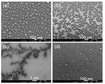
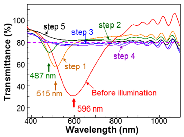
oC and is thermally stable. It can extend the transparent spectrum into ultraviolet and near-infrared ranges and can be applied to touch-panel displays, ultraviolet light-emitting diodes, and flexible optoelectronics devices. Figure 1(a) below shows the SEM image of the initial surface Ag NPs before illumination. Figures 1(b)-1(d) show the SEM images of the formed NNW structures with different magnifications after step-5 illumination. In Fig. 1(d), we show the SEM image in the clear area of the NNM structure, in which one can see the remaining low-density, small Ag NPs. Figure 2 shows the transmission spectrum of the sample after each illumination step. We can see that after step-5 illumination, the transmittance is always higher than 83% in the whole visible range.
|
 |
 |
|
Fig. 1 SEM images of an NNW structure. Fig. 2 Transmission spectrum after each illumination step. |
Quantitative spectroscopic comparison of the optical properties of mouse cochlea microstructures using optical coherence tomography
Professor Hsiang-Chieh Lee
Graduate Institute of Photonics and
Optoelectronics, National Taiwan University
Currently, the cochlear implantation procedure mainly relies on using a hand lens or surgical microscope, where the success rate and surgery time strongly depend on the surgeon’s experience. Therefore, a real-time image guidance tool may facilitate the implantation procedure. In this study, we performed a systematic and quantitative analysis on the optical characterization of ex vivo mouse cochlear samples using two swept-source optical coherence tomography (OCT) systems operating at the 1.06-µm and 1.3-µm wavelengths. The analysis results demonstrated that the 1.06-µm OCT imaging system performed better than the 1.3-µm OCT imaging system in terms of the image contrast between the cochlear conduits and the neighboring cochlear bony wall structure. However, the 1.3-µm OCT imaging system allowed for greater imaging depth of the cochlear samples because of decreased tissue scattering. In addition, we have investigated the feasibility of identifying the electrode of the cochlear implant within the ex vivo cochlear sample with the 1.06-µm OCT imaging. The study results demonstrated the potential of developing an image guidance tool for the cochlea implantation procedure as well as other otorhinolaryngology applications.
|
 |
|
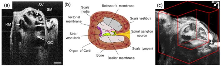
Fig. (a) Example cross-sectional OCT image of the mouse cochlea sample treated with ethylenediaminetetraacetic acid (EDTA) for 7 days, acquired with the 1.06 µm OCT system. RM: Reissner’s membrane; SV: scala vestibuli; SM: scala media; ST: scala tympani; OC: organ of Corti. Scale bar: 250 µm. (b) Schematic diagram showing the anatomic features of the mouse cochlea sample. (c) The volumetric rendering of three-dimensional OCT images of the cochlear sample. Red box: bounding box of the rendering. |
Reference:
Ting-Yen Tsai, Ting-Hao Chen, Hsin-Chien Chen, Chuan-Bor Chueh, Yin-Peng Huang, Yi-Ping Hung, Meng-Tsan Tsai, Bernhard Baumann, Chih-Hung Wang, and Hsiang-Chieh Lee, "Quantitative spectroscopic comparison of the optical properties of mouse cochlea microstructures using optical coherence tomography at 1.06 µm and 1.3 µm wavelengths," Biomed. Opt. Express 12, 2339-2352 (2021)
Effect of guard rings on the breakdown voltage of In0.53Ga0.47As/InP SAGCM avalanche
photodetectors
Professor Hao-Hsiung Lin’s Lab
Graduate Institute of Photonics and
Optoelectronics, National Taiwan University
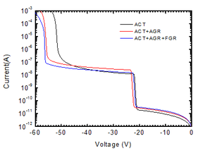
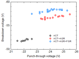
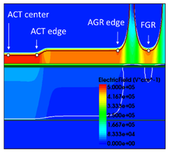
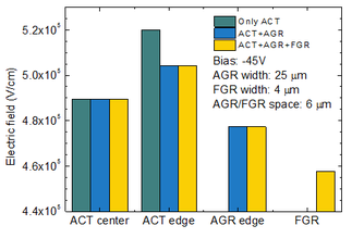
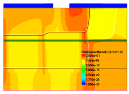
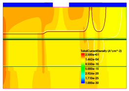
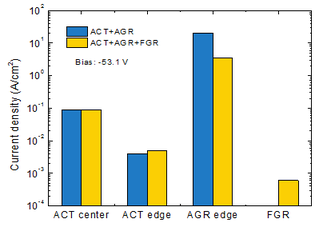
In0.53Ga0.47As/InP avalanche photodiodes (APD) with separate absorption, grading, charge, and multiplication (SAGCM) structure have been drawn attentions for the applications to LIDAR. In this work we studied the effect of attached guard ring (AGR) and floating guard ring (FGR) on the breakdown behavior of the APD. Fig. 1(c) shows the effect of AGR and FGR on the breakdown voltage. TCAD simulations for these structures were used to understand the mechanism. As shown in Fig. 2, the maximum electric field is located at the edge of active region and the GRs can decrease the electric field. Fig. 3 shows the current spreading in the devices with GRs. FGR can reduce the current at AGR edge and further improve the breakdown behavior.
|
 |
|
(a) |
|
 |
 |
|
(b) |
(c) |
|
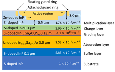
Fig. 1 (a) Schematic diagram of SAGCM APD with the epi-structure. (b) Typical photo I-V characteristics. (c) Breakdown voltages against the punch through voltages for APDs without GRs, with AGR only, and with AGR and FGR. |
|
 |
 |
|
(a) |
(b) |
|
Fig. 2 (a) Electric field contour plot of a simulated reverse bias APD with AGR and FGR. (b) Comparison of maximum electric field at center, active region edge, AGR edge, and under FGR for devices with different guard ring structures. |
|
 |
 |
|
(a) |
(b) |
 |
|
(c) |
|
Fig. 3 TCAD simulation of current density of devices (a) with AGR only, and (b) with AGR and FGR. (c) Comparison of maximum current densities at center, active region edge, AGR edge, and under FGR. |
Effects of Insulator Layer on
Metal-Si Midwave Infrared Photodetectors
Professor Ching-Fuh Lin
Graduate Institute of Photonics and
Optoelectronics, National Taiwan University
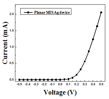
To overcome the limitation of Si bandgap on midwave infrared (MIR) detection, Schottky contact is a breakthrough to achieve longer wavelength detection. Schottky barrier by means of the contact of metal-semiconductor can reach a diode rectifying effect (Fig. 1.), and the oxide interlayer design provides better surface conditions for the junction and reduces Fermi-level pinning effect on the energy level.
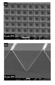
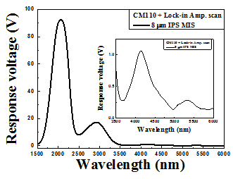
We accomplished a metal-insulator-semiconductor (MIS) device with an inverted pyramid structure (IPS), as shown in Fig. 2. The IPS design effectively enhances the light absorption of the device and can induce surface plasmon resonance to achieve MIR detection. The monochromator measurement from 1.5 μm to 6 μm light scan on the Ag/SiO2/n-Si device is shown in Fig. 3. Three wavelengths at 2.1, 3, 4.1 and 5.4 μm have response peaks. The responsivity at 3.46/4.26/5.30 μm are also measured, with values of 0.0410/0.0414/0.0188 mA/W, respectively.
|
 |
 |
|
Fig. 1. The I-V curve of the Ag MIS device |
Fig. 2. The SEM (a) top view and (b) section view of the IPS |
 |
|
Fig. 3. The monochromator scan of the device from 1.5~6 μm |
|
|
|
|
|
|
|
| |
|
|
 |
|
 |
|
|
|