|
September 2020 - November 2020 |
| |
|
|
 |
|
 |
| |
Publisher: Chairman Jian-Jang Huang Editors: Professor
Snow H. Tseng, Ms. Hsiao-wen Lin January 30, 2021 |
| |
|
 |
|
Congratulations to Prof. Chi-Kuang Sun, Prof. Yuh-Renn Wu, Prof. Ding-Wei Huang, Prof. Chao-Hsin Wu, Prof. Jian-Jang Huang, and Prof. Gong-Ru Lin for being awarded “Future Technology Award 2020.”
|
Affiliation
|
Technology |
Principal Investigator |
Co-Investigator |
|
National Taiwan University |
Harmonic Generation Microscopy |
National Taiwan University
Dr. Chi-Kuang Sun
|
|
|
National Taiwan University of Sport |
Karma Zone and Unmarked 3D Motion Analysis System |
National Taiwan University of Sport
Dr. Jyh-How Huang
National Taiwan University
Dr. Yuh-Renn Wu
|
National Taiwan University
Dr. Pei-Yuan Wu |
|
National Kaohsiung University of Science and Technology |
Next Generation 1.6Tb/s Silicon Photonics Chip |
National Kaohsiung University of Science and Technology
Dr. Tien-Tsorng Shih
|
National Taiwan University
Dr. Ding-Wei Huang
Dr. Chao-Hsin Wu
Dr. Jian-Jang Huang
Dr. Gong-Ru Lin
|
Congratulations to Shih-Chun Kao and Prof. Gong-Ru Lin for being awarded “Best Poster Award OECC 2020.”
|
Award Recipient
|
Advising Professor |
Research Topic |
|
Shih-Chun Kao |
Prof. Gong-Ru Lin |
Power Envelope Detection of 40-Gbit/s GFDM Data in Two-color VCSEL Based MMW-Oscillator-Free 5G Network |
Congratulations to Ya-Ting Liang and Prof. Chao-Hsin Wu for being awarded “Best Thesis Award OECC 2020.”
| Award Recipient |
Advising Professor |
Research Topic |
|
Ya-Ting Liang |
Prof. Chao-Hsin Wu |
Monolithically Integrated Opto-Electrical NOR Gate Using Light Emitting Transistors |
|
|
 |
|
 |
|
| |
|
|
~ Optoelectronics Summer Camp 2020 ~
(August 5-7, 2020,
Barry Lam Hall, National
Taiwan University)
By
Chih-Wei Huang
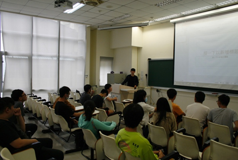
Every year, every summer, an Optoelectronics
Summer
Camp spanning over three days would be held at the Graduate Institute of Optoelectronics and Photonics. From morning to evening, from breakfast to supper, this Summer Camp is an introduction to the field of optoelectronics, open to all students with an interest in optoelectronics. Here, the attendants can experience first hand the newest developments at GIPO, along with all the excitements.
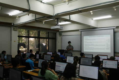
On the first day, an opening given by Prof. Jian-Jang Huang the Chairman of GIPO marked the beginning of the Optoelectronics Summer Camp, giving us a brief introduction on the background of optoelectronics and its developments, followed by three seminars given by Prof. Jui-Che Tsai, Prof. Guo-Dung Su, and Prof. Hoang-Yan Lin, on the topics of Laser Fundaments, Optical System Design with Zemax, and Embedded Systems respectively, giving us an in-depth understanding on laser optics and optical design.
|
 |
 |
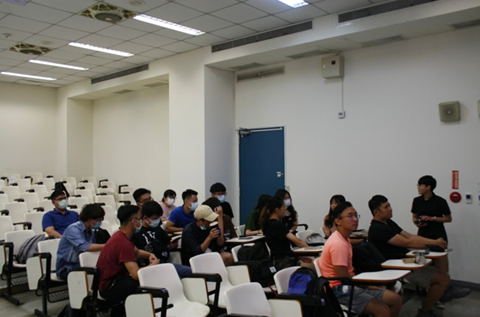
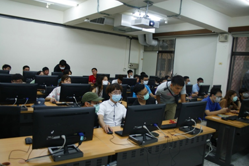
On the second day, Prof. Hsiang-Chieh Lee began the day with an introduction on photonics in biomedics, a rarely touched field especially while still at the undergraduate level. The goal of the Optoelectronics Summer Camp is to give the attendants an opportunity to gain some hands-on experience with the practical aspects of optoelectronics, and over the years the contents of the Summer Camp have undergone a series of reviews and developments. Today, the practical session was split into two parts. A Zemax workshop led by GIPO PhD candidate Chun-Yuan Fan, and a series of practical experiments on embedded systems designed by Prof. Hoang-Yan Lin and Prof. Ding-Wei Huang.
|
 |
 |
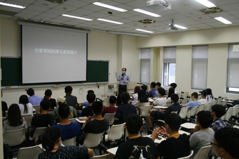
On the third day, Prof. Ding-Wei Huang gave us a talk on the basics of optical communication and its developments and evolution in industries, and the importance of its role in the future. At the end of the day, and also the end of the camp, we each shared our gains and thoughts over the past three days. Some of us were shy at first, and maybe a little uncertain, but as the sharing continued we reflected back more and more on the memories of the three days, which all of us remembered with fondness. Through this camp, we understood more about the field of optoelectronics, and we got to know more friends from different schools and places. To all of us, this camp has been an enjoyable and fulfilling experience.
|
|
|
|
|
| |
|
|
|
~ The 7th
Cross-Strait Workshop on
Wide
Band Gap Semiconductors ~
(October
22-23,
2020,
Barry Lam Hall, National Taiwan University)
By Yi-Lun Li
Due to COVID-19, this year was the first year that the scholars of the
7th Cross-Strait Workshop on Wide
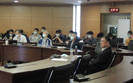
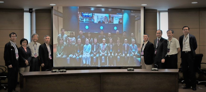
Band Gap Semiconductors were unable to meet and gather as planned. After much discussion on all sides, the conference was decided to be held online in two physical locations simultaneously, through video conference. On the day of the conference, more than 40 scholars from both sides of the Strait gathered online.
The goal of this conference was to stimulate the discussion of exchange of ideas between experts and scholars and industries from both sides of the Strait. The topics include Group III nitride semiconductors, II-VI semiconductors, oxide semiconductors, and manufacturing and applications. Scholars from both sides would take turns to present their findings, followed by in-depth discussions of the works presented.
 |

|
|
Fig. 1. Conference Photo |
Fig. 2. The conference opening, given by the conference chairman Prof. Jian-Jang Huang. |
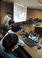
A successful video conference session is highly dependent on the computer equipment, cameras, and a fast and smooth network environment. As a person of average technological knowledge in those areas, I would like to thank the students of Prof. Jian-Jang Huang, the Chairman of GIPO and also the Chairman of this conference this year, for their generous assistance in operating the conference equipment and overseeing the running of the conference. A special thanks to Ms. Pei Chang too.
On the first day of the conference, the first session begins on 7:30 AM. Even before 6:30 AM, the students were gathered in full already, and we had breakfast together, of toasts and an assortment of dips and spreads. At the end of the conference, we chattered and laughed as we packed and returned the venue to normal, and Prof. Jian-Jang Huang stayed with us until the very end. It was a wonderful feeling, being a part of the team.
 |
 |
|
|
Fig. 3. The main control desk and the desk operator. |
Fig. 4. A seminar given by Prof. Jian-Jang Huang. |
Fig. 5. Toasty morning. |
During one of the tea breaks, one of the visiting scholars mentioned to us, “We were only coming for two days, but your team has prepared for this for over a month!” Here, a special thanks goes to the Center for Teaching and Learning Development
& Digital Learning Center for the provision of the conference equipment, and for many of their invaluable advice on online video conferencing, as well as the institute staff
members and Ms. Pei Chang for their assistance in overseeing the conference. A big thank you to the students of Prof. Jian-Jang Huang for sacrificing their valuable time outside their studies, and the network administrator of the Department of Electrical Engineering and Barry Lam
Hall overseers for their help. It was with your help that we still managed to hold a successful conference despite this slightly out of the ordinary year.
|
|
|
Fig. 6. Conference group photo of all scholars on both sides of the screen and both sides of the Strait. |
|
|
|
|
|
|
| |
|
|
|
Formation of ceramic and crystal claddings for Ti:sapphire crystalline fiber core
Professor Sheng-Lung Huang
Graduate
Institute of Photonics and
Optoelectronics, National Taiwan
University
Fibers with crystalline core and clad have high potential for high power applications. When compared with the photonic crystal fibers with glass core, the single-crystalline-core fiber has, in general, a higher melting point and larger dielectric breakdown field, that make it advantageous for high power light source applications. However, most of the crystal-core fibers use glass as a cladding, which are still affected by the fringe field. Air-cladding can avoid this damage, but it induces high losses. Using ceramic or crystal cladding, power can be scaled up without damaging the fiber while keeping a low transmission loss. For single-mode structures the laser intensity and the amplified spontaneous emission can be maintained at high level, whereas for optical amplification, it is essential to use single-mode waveguiding to achieve high signal gain.
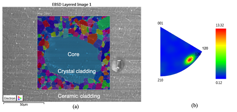
In this study, we have developed single-mode Ti:sapphire crystalline fibers, cladded by dip coating and high-temperature sintering at 1750 °C. Solid-state single crystal growth was observed at the perimeter of the crystalline core, and the growth speed along (11 ̅0) is about 2.7 times faster than that of (001). As shown Fig. 1, the grown cladding was single-crystalline as evidenced by electron backscattered diffraction and scanning electron microscopy examinations. From optical transmission measurement at 1550 nm, the far-field distribution of the transmitted light matches well with that of the fundamental mode. With a core size of 30 μm, the refractive index difference between core and clad was measured to be 1.0x10⁻⁴. From fluorescence mapping on the fiber end face, a very limited amount of the Ti3+ ions in core were diffused into the grown crystalline cladding during the solid-state growth. The realization of a fully crystalline single-mode fiber could be useful for applications where high power and/or high brightness light sources are needed.
|
|
|
Fig. 1. (a) EBSD end-face image of ceramic crystal cladded fiber, which was sintered for 24 hours at 1650 °C, and (b) crystal orientation map displayed in inverse pole figure coloring. |
Reference:
T. I Yang, H. T. Liu, S. C. Wang, K. H. Chuang, T. C. Chou, and S. L. Huang, “Formation of ceramic and crystal claddings for Ti:sapphire
crystalline fiber core,” Opt. Materials Express,
10,
No. 5, pp. 1215–1223, 2020.
Development of mesoscopic nonlinear imaging system with record-dense sampling capability
Professor Chi-Kuang Sun
Graduate
Institute of Photonics and
Optoelectronics, National Taiwan
University
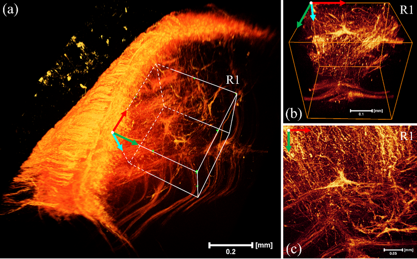
Nonlinear imaging [1] of volumetric biological specimens can reveal its three-dimensional (3D) structural details with ultra-high spatial resolution, in terms of depth-resolved cross-sectional views with a better penetration capability due to the use of near-infrared (NIR) excitation spectrum and excitation localization of nonlinear optical absorption, in comparison to single-photon based imaging modalities. To facilitate high-speed, but aliasing-free laser-scanning of a centimeter-scale volumetric sample, an ultra-large field of view (FOV) is mandatory, which must be digitized with an ultra-fast sampling rate in order to fulfil the Nyquist Criterion, being a fundamental limitation to all the state-of-the-art mesoscopic imaging systems to date [2].
Our group has developed a nonlinear optical mesoscope (NLOM) with an extended FOV of up-to 1.6×1.6 mm2 while preserving a smallest resolvable spacing of 0.48 μm. We further introduced a one-pulse-per-voxel extreme-synchronized-sampling for the first time in an NLOM with a FOV/ resolution ratio over 3000. Our record acquisition system holds the capability of simultaneously sampling 4 channels at up-to 125 MSps sampling-rate, reaching a record single-frame pixel number of 15720×16000 for each of the 4 channels, leading to a total of ~1 Gigapixels per frame, while maintaining ~0.5 fps; including real-time calibration, preview and storage of the acquired data in 16-bit format with 14-bit resolution.
|
|
|
Fig. 1(a) 3D view of coronal sections from medulla of a Nav1.8-tdTomato mouse; (b), (c) zoomed views of ROI R1 in (a). Red, green & cyan axes are X, Y & Z axes, respectively. Scale bars: (a) 0.2 mm, (b) 0.1 mm, (c) 0.05 mm. |
Reference:
1. W.
R. Zipfel, R. M. Williams, W. W. Webb,
Nonlinear magic: multiphoton microscopy
in the biosciences. Nature
biotechnology, 21,1369–1377 (2003).
2. M.
Balu, H. Mikami, J. Hou, E. O. Potma, B.
J. Tromberg, Rapid mesoscale multiphoton
microscopy of human skin. Biomedical
Opt. Express 7, 4375-4387 (2016).
Study on the Design Parameters for Curved-Type Parallax-Barrier Dual-View Display
Professor Hoang-Yan Lin
Graduate
Institute of Photonics and
Optoelectronics, National Taiwan
University
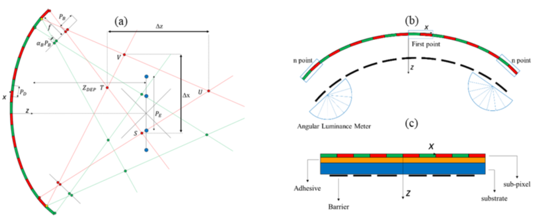
The 3D stereoscopic display makes both eyes to see the left and right image information separately, and recombine them to create stereoscopic vision. The dual-view display distributes the left and right images to each viewing zone, which can be realized through spatial multiplexing methods. The image information can be divided into different position by adding the parallax-barrier or lenticular-lens structures on the display system. The difference between the dual-view and 3D stereoscopic displays is that the viewing position is changed from the distance between both eyes of a person to the double viewing zones which can be designed by yourself. It becomes a technology that can provide at least two users on a single display at the same time. In recent years, the advancement of flexible substrate technology has brought attention to the issue of curved display. Curved displays provide screen-enlarged perception and immersive vision experience.
For the dual-view display, viewing position and the range nearby strongly affect image quality. Viewing zone describes the spatial range in front of the display where a viewer could move around while experiencing the corresponding image information. Regarding a curved dual-view display, radius and viewing angle of the screen determine the relative degrees of bending, by which the spatial light distribution can be determined. In addition, this is a key factor influencing image quality, especially for the display which directs the views for left and right viewing zones based on different image information. By using geometric optics and ray-tracing software, the viewing zone can be calculated and depicted, and discussed as given different curvature radius or viewing angle of the screen with refractive index substrate. Considering crosstalk and uniformity, we present a method to control the viewing zones by shifting parallax barrier in this study.
A curved-type parallax barrier dual-view display was constructed and shown as in Fig. 1(a). PD and PB are the pitches of the sub-pixel on display and the barrier aperture, respectively. A distance from the display to barrier is defined as f, a distance from barrier to a viewer is defined as ZDEP, and the dual people distance (DPD) is marked as PE. The geometric relationship is similar to our preview study for 3D stereoscopic displays. First, we take the emitting light rays through the sub-pixel edge to intersect in front of the display. Considering the radius of curvature, the design viewing positions on the left and right must be rotated into a plane parallel to the sub-pixels. The line of intersection point is the barrier, and the opening position of it can be calculated from the period of the barrier. By connecting the edge sub-pixels with the opening position of the parallax barrier, the right viewing zone, corresponding points STUV, can be calculated and depicted. ∆x and ∆z are the width and depth of the viewing zone, respectively. The left viewing zone can calculated an depicted in the same way.
Considering crosstalk and uniformity, it is defined that the crosstalk value must be less than 10%. Under the condition, the received image information will not be blurred or distorted. The uniformity value must be greater than 60%. Human eyes face the entire screen so that there is no uneven brightness problem. Spatial luminance distribution of the right viewing zone is shown as Fig. 2, (a) without considering crosstalk and uniformity, and (b) with crosstalk and uniformity situation.
|
|
|
Fig. 1. Construction of curved type parallax barrier dual-view display |
|

|
|
Fig. 2. Spatial luminance distribution of the right viewing zone |
Reference:
Yen-Wen Lin, Wei-Chen Chen, Hoang Yan Lin, Study
on the Design Parameters for Curved-Type
Parallax-Barrier Dual-View Display, submitted to
OPTIC 2020.
Synthesizer-free 28-GHz MMW Fiber-wireless Link with Orthogonally Polarized Dual-mode VCSEL
Professor Gong-Ru Lin’s Laboratory
Graduate Institute of Photonics and
Optoelectronics, National Taiwan
University
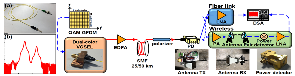
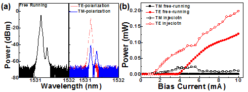
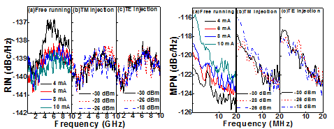
A synthesizer-free 28-GHz is proposed for fifth-generation (5G) millimeter wave over fiber (MMWoF) link by using orthogonally polarized dual-mode vertical-cavity surface-emitting laser (VCSEL) as the frontend transmitter, and the power envelope detection is employed for self-heterodyne down-conversion of the generalized frequency division multiplexing (GFDM) data stream. The demonstrated MMWoF link exhibits superior immunity to the residual frequency and phase noises as well as the inter-carrier interference induced by the free-running dual-mode carrier. After equalizing the dual modes with an extremely weak power as low as -26 dBm at TM-mode polarization, the dual-mode power extinction of only 5.4 dB is achieved for optimizing the remote-node optical heterodyne of 28-GHz MMW carrier with a peak power of -59.8 dBm before antenna propagation with remaining similar relative intensity noise (RIN) as compared to the free-running case. Moreover, the mode partition noise (MPN) is increased less than 2 dBc/Hz after mode-power equalization.
|
|
|
Fig. 1 Schematic diagram of 5G MMWoF link based on 2-l VCSEL transmitter with novel QAM-GFDM.
(a) The photograph and (b) the optical spectrum of 2-l
VCSEL without package. |
 |
|
|
Fig. 2 (a) The free-running polarization characteristic and (b) the P-I curves without and with master controlling of the dual-mode VCSEL. |
Fig. 3 The RIN and MPN of the dual-mode VCSEL at (a) free-running operation with different bias current and (b) TE- (c) TM-mode injection controlling. |
For back-to-back optical downstream wireline transmission, the receiving GFDM data optimizes its BER to 2.2´10-4 by adjusting the bias current of the dual-mode VCSEL to 8 mA (3 Ith), and by grouping the GFDM data matrix with total symbols of
N=K´M with
K=2 subcarriers and
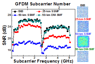
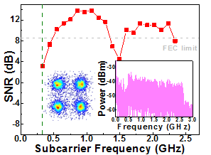
M=24 timeslots. After long-reach 50-km DM-SMF, the qualified receiving power sensitivity is -12 dBm, whereas the decoding GFDM data reveals improved receiving sensitivity with extremely low power penalty of only 0.3 dB. After wireless delivering over 2 m in free space, the self-heterodyne down-conversion by power envelope detection guarantees the down-converted QAM-GFDM data stream with an average power of -48.4 dBm after optimizing the impedance matching by selecting appropriate frequency response of the power envelope detector. As a result, the wireless MMW transmission of 8-Gbit/s 4-QAM GFDM data stream is qualified with EVM of 16.9%, SNR of 8.5 dB and BER of 3.8´10-3.
 |
|
|
Fig. 4 The constellation plots and decoded SNR spectra of the modulated 30-Gbit/s 64-QAM GFDM data by the dual-mode VCSEL after BtB, 25-/50-km SMF and 50-km DM-SMF transmissions. |
Fig. 5 The constellation plot, RF and SNR spectrum of the delivered 4-QAM GFMD data after 2-m free-space transmission and self-heterodyne down-conversion. |
Reference:
[1] C.-Y. Lin, Y.-C. Chi, C.-T. Tsai, H.-Y. Wang and G.-R. Lin, “39-GHz millimeter-wave carrier generation in dual-mode colorless laser diode for OFDM-MMWoF transmission,”
IEEE
J. Sel. Top. Quantum Electron.,vol. 21, no. 6, pp. 609-618, 2015.
[2] C.-T. Tsai, C.-H. Lin, C.-T. Lin, Y.-C. Chi and G.-R. Lin, “60-GHz millimeter-wave over fiber with directly modulated dual-mode laser diode,”
Sci Rep, vol. 6, no. 27919, pp. 1-12, 2016.
[3] C.-Y. Lin, Y.-C. Chi, C.-T. Tsai, H.-Y. Wang, H.-Y. Chen, M. Xu, G.-K. Chang and G.-R. Lin, “Millimeter-wave carrier embedded dual-color laser diode for 5G MMW of link,”
J. Light. Technol, vol. 35, no. 12, pp. 2409-2420, 2017.
[4] C.-Y. Lin, Y.-C. Chi, C.-T. Tsai, H.-Y. Chen and G.-R. Lin, “Two-color laser diode for 54-Gb/s fiber-wired and 16-Gb/s MMW wireless OFDM transmissions,”
Photonics Res., vol. 5, no. 4, pp. 271-279, 2017.
[5] Z.-K. Weng, Y.-C. Chi, H.-Y. Kao, C.-T. Tsai, H.-Y. Wang and G.-R. Lin, “Quasi-color-free LD-based long-reach 28-GHz MMWoF With 512-QAM OFDM,”
J. Light. Technol., vol. 36, no. 19, pp. 4282-4297, 2018.
A New Fitting Method for Ambipolar Diffusion Length Extraction in Thin Film Structures Using Photoluminescence Measurement with Scanning Excitation
Professor Ming-Hua Mao’s Laboratory
Graduate
Institute of Photonics and
Optoelectronics, National Taiwan
University
A new simple method is proposed to extract the
ambipolar diffusion length for two-dimensional (2D) electronic transport in thin
film structures using a scanning photoluminescence microscopy (SPLM) setup. No
spatially-resolved photoluminescence detection methods are required. By
measuring the excitation-position-dependent PL intensity across the edge of a
semiconductor, ambipolar diffusion length can be extracted from the SPLM profile
through a simple analytic fitting function. Numerical simulation was first used
to verify the fitting method. Then the fitting method was applied to extract the
ambipolar diffusion length from the measured SPLM profile of a GaAs thin film
structure. Carrier lifetime was obtained in an accompanying time-resolved
photoluminescence measurement under the same excitation condition, and thus the
ambipolar diffusion coefficient can be determined simultaneously. The new
fitting method provides a simple way to evaluate carrier transport properties in
2D electronic transport structures such as thin films or quantum wells. This
work has been published in Scientific Reports: Chu, C. H., Mao, M.-H., Lin, R.
Y. & Lin, H. H. A New Fitting Method for Ambipolar Diffusion Length Extraction
in Thin Film Structures Using Photoluminescence Measurement with Scanning
Excitation.
Scientific Reports
10,
5200, doi:10.1038/s41598-020-62093-w (2020).
|
 |
|
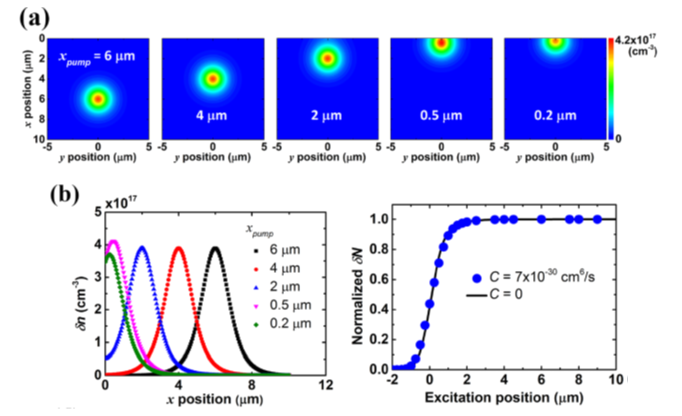
Fig. 1 (a) 2D photocarrier distribution mappings under CW excitation with varied excitation position (x,y) = (xpump,0). (b) Cross-sections of the above mappings at
y = 0 & scanning profile for the normalized total photocarrier number
δN under pulse excitation. The result without Auger recombination is also shown for comparison. |
|
|
|
|
|
|
|
| |
|
|
 |
|
 |
|
|
|