|
November
2019 - February 2020 |
| |
|
|
 |
|
 |
| |
Publisher: Chairman Jian-Jang Huang Editors: Professor
Snow H. Tseng, Ms. Hsiao-wen Lin April 30, 2020 |
| |
|
 |
|
Congratulations to Prof. Gong-Ru Lin for being awarded “2020 IEEE Fellow.”
Congratulations to Prof. Lon A. Wang, Prof. Chung-Chih Wu, Prof. Guo-Dung Su, Prof. Yuh-Renn Wu, and Prof. Hsiang-Chieh Lee for representing Team EECS and achieving Third Place in “2019 Academic Year NTU Staff Inter-Department Softball Tournament.”
Congratulations to our PhD candidate for being awarded “2019 CITI Foundation Technology Sector Scholarship.”
|
Award Nominee
|
Adviser |
Scholarship |
|
Pan Li |
Prof. Chung-Chih Wu |
2019 CITI Foundation Technology Sector Scholarship - PhD |
Congratulations to the following students for the award of “OPTIC 2019 Student Paper Award.”
|
Award Recipient
|
Award |
Adviser |
|
Pei-Jhe Wu |
OPTIC 2019 Student Paper Award (PhD)
Thesis title: Harmonic Generation Microscopy for Assessment of the Histopathological Characteristics and Therapeutic Outcome for Acquired Bilateral Nevus of Ota-like Maculae (ABNOM)
|
Prof. Chi-Kuang Sun |
|
Chen-Ling Wu |
OPTIC 2019 Student Paper Award (Master)
Thesis title: The Ultra-Short Photoacoustic Pulse Generation Using 2-Dimensional Electron Gas |
Prof. Chi-Kuang Sun |
|
Yang-Ting Hsiao |
OPTIC 2019 Student Paper Award (Master)
Thesis title: High Power Fiber-Format Femtosecond Laser for Simultaneous Three-Color Excitation of Two-Photon Microscopy
|
Prof. Chi-Kuang Sun |
|
Meng-Yu Tsai |
OPTIC 2019 Student Paper Award (Master)
Thesis title: GHz Optical Frequency Modulation from Light Emitting Diodes by Surface Acoustic Waves
|
Prof. Jian-Jang Huang |
|
Tsung-Jung Chuang |
OPTIC 2019 Student Paper Award (Master)
Thesis title: Polarization-independent metalens via modulating nanobar height ratio at visible wavelength
|
Prof. Guo-Dung Su |
|
Cheng-Fu Hsu |
OPTIC 2019 Student Paper Award (Master)
Thesis title: a-IGZO Thin-Film Transistor-Based Differential Amplifier
|
Prof. I-Chun Cheng
|
|
Yun-Ting Huang |
OPTIC 2019 Student Paper Award (Master)
Thesis title: Monolithically Integrated Optical NOR Gate Using Light-Emitting Transistors
|
Prof. Chao-Hsin Wu
|
|
Ching-Yu Wang |
OPTIC 2019 Student Paper Award (Master)
Thesis title: Investigation of the ex vivo Mouse Brain Tissue Architecture with a Long Wavelength Optical Coherence
|
Prof. Hsiang-Chieh Lee |
|
|
 |
|
 |
|
| |
|
|
|
October “GIPO Colloquium” Highlights
(Compiled by Li-Chi Yao) |
|
|
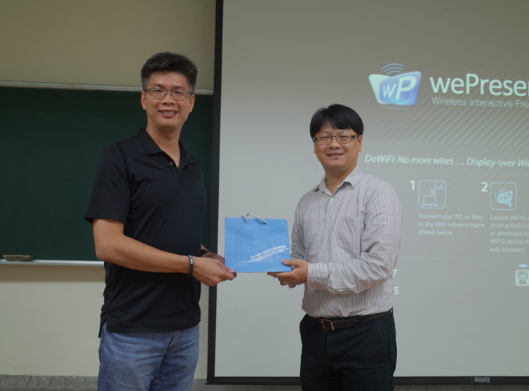
2:20 pm, Oct.
18 (Fri.), 2019 |
|
Speaker: |
Assistant Executive Officer IC Jan (National Biotechnology Research Park, Academia Sinica) |
|
Topic: |
A Life of Enterprising and Investments |
| |
|
 |
|
Assistant Executive Officer IC Jan (left) and Prof. Hsiang-Chieh Lee (right) |
|
|
November “GIPO Colloquium” Highlights
(Compiled by Li-Chi Yao) |
|
|
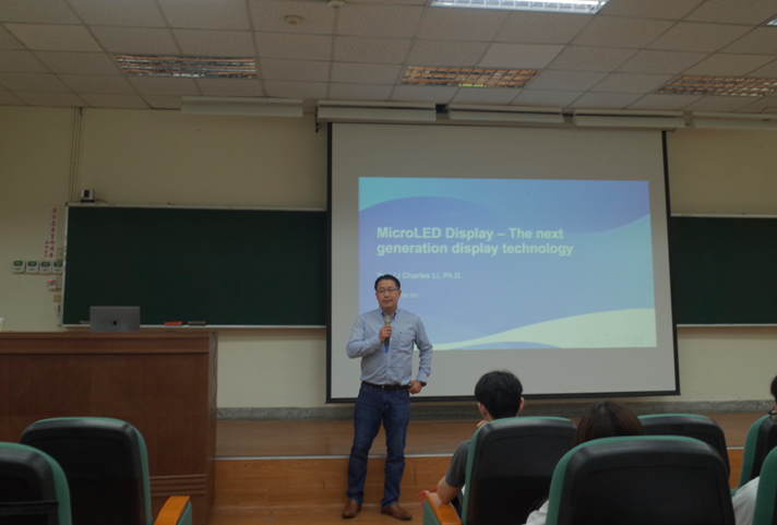
2:20 pm, Nov.
1 (Fri.), 2019 |
|
Speaker: |
Dr. Yun-Li Li (CEO of PlayNitride Inc.) |
|
Topic: |
MicroLED Display - the Next Generation Display Technology |
|
|
|
 |
|
Dr. Yun-Li Li, CEO of PlayNitride Inc. |
|
|
|
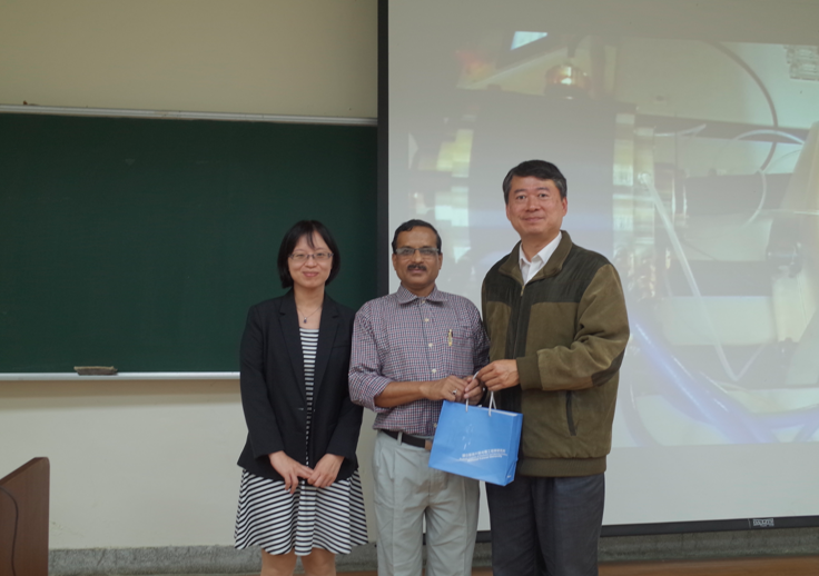
2:20 pm, Nov. 8 (Fri.), 2019 |
|
Speaker: |
Dr. Mukul Chandra Paul (Principal Scientist/Associate Professor, Fiber Optics and Photonics Division, Central Glass and Ceramic Research Institute, India) |
|
Topic: |
Research and development activities at Fiber Optics and photonics Division from view point of development of specialty optical fiber and fiber-based photonics devices |
|
|
|
 |
|
Dr. Mukul Chandra Paul (middle) and Prof. Sheng-Lung Huang (right) |
|
|
|
2:20 pm, Nov. 22 (Fri.), 2019 |
|
Speaker: |
Patent Attorney Mr. Narvis Wu (Wood & Wu Patent and Trademark Office) |
|
Topic: |
Different Ways of Profiting from Technology Patents |
| |
|
 |
|
Patent Attorney Mr. Narvis Wu (left) and Prof. Hoang-Yan Lin (right) |
|
|
December “GIPO Colloquium” Highlights
(Compiled by Li-Chi Yao) |
|
|
2:20 pm, Dec.
13 (Fri.), 2019 |
|
Speaker: |
Prof. Xiuling Li (Department of Electrical and Computer Engineering, University of Illinois) |
|
Topic: |
Nanostructured Materials and Devices: Innovations for Electronic, Photonic, and Biomedical Applications |
|
|
|
 |
|
Prof. Xiuling Li (left) and Prof. Chao-Hsin Wu (right) |
|
|
|
2:20 pm, Dec. 20 (Fri.), 2019 |
|
Speaker: |
Prof. Wei-Chieh Tseng (Department of Chinese, National Taiwan Normal University) |
|
Topic: |
Courage for Immorality - Modern Psychology and Social Media |
|
|
|
 |
|
Prof. Wei-Chieh Tseng (left) and Prof. Hsiang-Chieh Lee (right) |
|
|
|
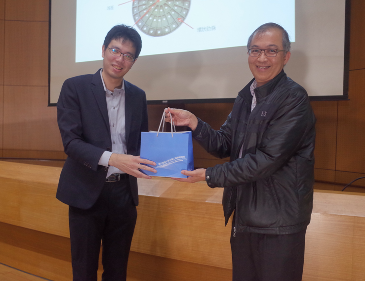
2:20 pm, Dec. 27 (Fri.), 2019 |
|
Speaker: |
Vice Chairman Mr. Yu-Chi Wang (WIN Semiconductors Corp.) |
|
Topic: |
New Era of III-V Semiconductor OEM |
| |
|
 |
|
Vice Chairman Mr. Yu-Chi Wang (right) and Prof. Jian-Jang Huang (left) |
|
|
|
|
|
|
| |
|
|
|
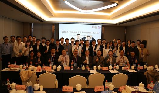
~ 2019 Ph.D. Student Academic Exchange with Nanjing University
~
(The 12th
Cross-Strait Ph.D. Student Forum on Photonic Science and Technology, 2019)
(Time: Nov.18-22 , 2019;
Location: Nanjing University)
Composed by
Ting-Hao Chen,
GIPO Ph.D. student
The 12th Cross-Strait
Ph.D.
Student Forum on Photonic Science and
Technology 2019
was held between 18th to 22th November, 2019. The conference period took place between the 19th and 20th November, at a hotel conference hall located in Nanjing Jiangbei New Area. On the morning of the 19th, the conference chairman Prof. Xinglong Wu (Vice Department Head of School of Physics, Nanjing University) opened the conference by introducing and handing the opening of the conference to the Vice Principal of Nanjing University, Prof. Zhenlin Wang. After the opening, the PhD forum began. The first morning of the forum comprised mainly of introductions of the invited speakers made up of members of the faculty from both sides, followed by their presentations. This year, the conference was able to invite the founders of this cross-strait forum, Prof. Shining Zhu of Nanjing University and Prof. Chih-Chung Yang of National Taiwan University, to impart upon the younger forum participants their research and their findings. The special topic given by Prof. Zhu’s research team on the unmanned observation of quantum entanglement and communication, and Prof. Yang’s student’s findings on surface silver nano network structures, were two deeply entrancing and valuable talks.
Other than PhD candidates from Nanjing University and National Taiwan University, other participants include students from Nanjing University of Aeronautics and Astronautics, Nanjing Normal University, and Soochow University, numbering at 32 in total. The presentations ranged from topics including inorganic display technology, solar energy material and components, nonlinear optics, topological optics, quantum optics and communication, III-V semiconductor components, liquid crystal application, light guide design, and biomedical optoelectronics system design. Topics on display technology and III-V semiconductors were two common interests of this forum, and many presenters shared their research findings with the forum participants. Research findings on nonlinear optics, topological optics, and quantum optics and communication were mainly presented by forum participants from Nanjing University. In particular, the presentation by Mr. Hong-Fei Wang on topological optics applications in photonic crystals, caught my attention. In the following days after the forum, Mr. Wang and I exchanged many ideas and thoughts, and we were both able to benefit from this exchange.
On the other hand, topics on the applications of liquid crystal, light guide design, and biomedical optoelectronics system design were presented by participants from National Taiwan University. One particular presentation by Mr. Chan-Yuan Fan of National Taiwan University, on the combination of utilization of liquid crystal and metalens to form a varifocal and aberration adjustable optical component, attracted interest from fellow students and professors alike. Another notable mention was that in my own research field of biomedical optoelectronics systems, Ms. Yaoyao Shi also presented a topic closely related to my field, however with a completely different direction of application, which greatly attracted my interest. Her research utilizes decorrelation image processing technology on the image formation of biological organisms and image encryption, which broadened my understanding of the scope of my research field.
The Popularity Awards of this forum went to Ms. Xinyu Huang of Nanjing University and Mr. Chia-Chun Ni of National Taiwan University. Both their research presentations were well received among student participants and faculty members of both universities alike. In particular, Ms. Xinyu Huang’s research achievements were documented on Nature Communication, a world renowned and recognized journal of this research field. The Best Thesis Awards went to Mr. Guang-Xu Su of Nanjing University, for his research on novel nanomaterial and two-dimensional structures, and Mr.Teng-I Yang of National Taiwan University on the application of crystalline optical fiber and developments in broadband light source. Both were remarkable achievements. Personally, it is my opinion that this forum greatly benefits all participants, in sharing of academic findings among like-minded intellects, broadening our views and the scope of our research, and serves as a beaconing encouragement in academic exchange and growth for both of us. I thank the many faculty members and fellow students of Nanjing University involved in the organization of this impeccably wonderful exchange event.
|
 |
 |
|
Prof. Chih-Chung Yang of National Taiwan University, and Prof. Xinglong Wu, the Vice Department Head of School of Physics, Nanjing University |
Prof. Jian-Jang Huang, Chairman of Graduate Institute of Photonics and Optoelectronics, National Taiwan University, and Prof. Shining Zhu of School of Physics, Nanjing University |
|
 |
|
Closing group photo |
|
|
|
|
|
|
| |
|
|
|
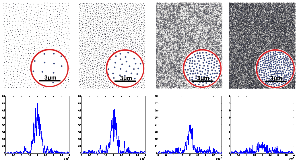
Simulating light transmission through scattering medium via numerical solutions of Maxwell’s equations
Professor Snow H. Tseng
Graduate
Institute of Photonics and
Optoelectronics, National Taiwan
University
Human cornea and sclera have very similar structures but distinctive optical characteristics. Here we model monochromatic light propagation through a macroscopic scattering medium by employing the pseudospectral time-domain (PSTD) simulation technique. We analyze the transparency; various factors are investigated. By analyzing the transmitted light intensity, the research objective is to decipher factors that contribute to the corneal and scleral optical characteristics.
|
 |
|
Figure 1. Simulation analysis of the transmitted light intensity through scattering media of various cylinder spacing. Wavelength of the CW light is
λ = 538 nm. (Upper row): the scattering medium consists of 200-nm-diameter dielectric cylinders. (Lower row): The light amplitude exiting the scattering medium. The penetrated light intensity decreases with increased cylinder diameter. |
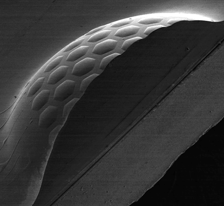
Biologically based artificial compound eye designed for a camera lens
Professor Guo-Dung J. Su
Graduate Institute of Photonics and
Optoelectronics, National Taiwan University
TAIPEI, TAIWAN — Researchers have designed a new camera module that uses a curved hexagonal microlens array and all spherical surfaces. Traditionally camera designs are difficult to assemble due to tight tolerance, because they consist of many separated lenses. If there is only one lens element in the camera, tolerance buildups can be avoided. The way to achieve a one-lens camera is through combining many lenses.
Researchers led by Prof. Guo-Dung J. Su from the Micro Optics Device Laboratory of the Graduate Institute of Photonics and Optoelectronics at National Taiwan University, Taiwan, experimentally demonstrated a one-lens camera design using a biologically inspired artificial compound eye with multiple focal lengths to avoid tolerance buildups. The artificial compound eye is a curved hexagonal microlens array arranged across a hemispherical photopolymer dome, wherein each microlens collects light with a small angular acceptance.
|
 |
|
Fig. 1. SEM images of the one-lens camera module system using a curved hexagonal microlens array attached to a hemispherical lens. The oblique view after cutting with a dicing saw is used to confirm the fabricated curved microlens array is spherical and its center of curvature locates at the down surface of the glass substrate. Image taken by Wei-Lun Liang, National Taiwan University. |
“This structure is integrated by the principles of both the human eye as well as an insect’s compound eye. It helps us to achieve a compact and wide field-of-view camera module.” said Wei-Lun Liang of the Micro Optics Device Laboratory, who was instrumental in designing the one-lens camera. “Most camera sensors are flat, due to the lithographic fabrication process. Our research showed that the field curvature aberration can be reduced by focusing on the best way to project a sharp image onto a flat surface.”
There are several benefits of using a hemispherical lens for a camera system, such as avoidance of coma aberration, wide field-of-view collection, and reduction of astigmatism aberration. However, a common optical problem of a hemispherical lens is known as field curvature aberration, and its image plane can be referred to as a curved Petzval surface. If the microlens array is arranged on the hemispherical surface, it can help with solving the problem.
To create the one-lens camera, the researchers used inkjet printing technology with the hydrophilic confinement effect to establish microlens shapes with different profiles on a planar substrate. The replication process can convert the planar array into a curved shape. Next, liquid photopolymer is filled into a deformed elastomer membrane and then cure when exposed to ultraviolet light. In the end, the spherical configuration of the hexagonal array of multiple focal lengths is accomplished by applying the template architecture to a reconfigurable surface shape.
To verify that the fabricated lens has hemispherical shape, the researchers observe scanning electron microscope (SEM) images of the lens sectioned by a dicing saw. “The sample is fed into a high-precision dicing saw, and the cutting blade accurately passes through the centers of the microlenses,” said Liang. “From the SEM images, we can check that the curved array is spherical and its center locates on the planar side of the lens.”
After an image is captured by the experimental setup of the camera module system which is built up of the one lens component, the researchers stitch every partial image formed by each microlens within its segmented channel into a combined image. “Tracing the path of a light beam emitted from a point source toward the image plane, the rays of the light beam pass through neighboring microlenses and produce several convergent beams of light.” said Liang. “This phenomenon leads to duplicate regions in neighboring sub-images, and these duplicate regions become a benefit for the subsequent image stitching.”
The researchers are now managing to convert their design into a commercial product. The funding support is from Taiwan Ministry of Science and Technology (MOST).
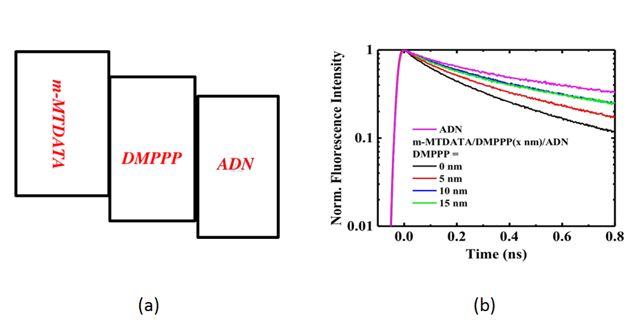
Exciton dynamics in tri-layer organic thin-film with exciplex sensitized triplet-triplet annihilation
Professor Jiun-Haw Lee
Graduate Institute of Photonics and
Optoelectronics, National Taiwan University
Exciton dynamics in tri-layer organic thin-film with exciplex sensitized triplet-triplet annihilation (ESTTA) process was studied by transient photoluminescence (trPL) measurement, which consists of 4,4’,4’’-tris(N-3-methyphenyl-N-phenyl-amino)triphenylamine (m-MTDATA) acting as the electron donor, 1-(2,5-dimethyl-4-(1-pyrenyl)phenyl)pyrene (DMPPP) as a triplet-diffusion-singlet-blocking (TDSB) layer, and 9,10-bis(2’-naphthyl) anthracene (ADN). With increasing the thickness of DMPPP from 0, 5, 10, and 15 nm, fluorescence decay time increased which was closed to the ADN thin-film, because DMPPP effectively blocked the singlet quenching of ADN by DMPPP.
|
|
|
Fig. 1. (a) Energy diagram of tri-layer organic thin-film, and (b) trPL measurement of thin film with different DMPPP thicknesses. |
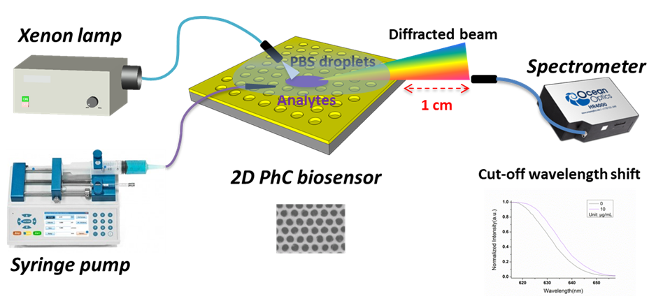
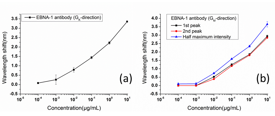
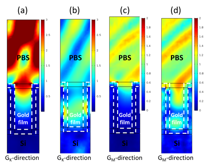
Surface plasmons coupled two-dimensional photonic crystal biosensors for Epstein-Barr virus protein detection
Professor Jian-Jang Huang
Graduate Institute of Photonics and
Optoelectronics, National Taiwan University
The fundamental detection scheme of typical grating or photonic crystal (PhC) sensors relies on the correlation of the diffraction behaviors with the refractive index of target analyte. For biomaterial detection, a thin gold film is usually deposited on the sensor surface so that cross linkers can be anchored before functionalizing the device. The nanoscale metallic film suggests plasmonic resonances play a critical role in light-matter interaction. In this work, we demonstrated a compact two-dimensional (2D) hexagonal photonic crystal (PhC) biosensor with thin gold film coating. In such a device, surface plasmon polariton (SPP) on the metal structure and phase matching of optical wave with the PhC are considered when analyzing light-biomaterial interaction on the detector. Using Epstein-Barr nuclear antigen-1 (EBNA-1) antibody as an example, protein sensing along different lattice orientations of the PhC biosensor was investigated. Based on the dispersion relationship and phase matching conditions, we unravel the mechanisms involved in the wavelength shifts and sensitivities. The simulation results verify the phenomenon of tighter spatial confinement and higher local field intensity from the SPP, which helps detecting small variations of the refractive index on the sensor surface.
|
|
|
Fig. 1. Experimental setup for characterizing EBNA-1 antibodies |
|
|
|
Fig. 2. (a) Sensitivity curves (cut-off wavelength shifts of various EBNA-1 antibody concentrations) along (a) Gk and (b) Gm directions |
|
|
|
Fig. 3. Simulation results of a EM field within a single nanohole |
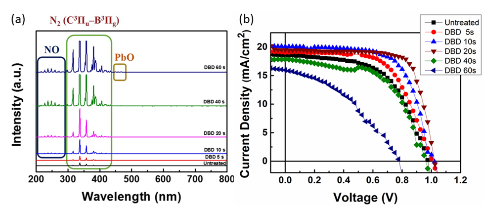
In-situ CH3NH3PbI3 Interface Treatment by Dielectric Barrier Discharge Plasma for Perovskite Solar Cells
Professor I-Chun Cheng
Graduate Institute of Photonics and
Optoelectronics, National Taiwan University
The surface diffusion dielectric barrier discharge (SDDBD) is a type of low-temperature plasma operated at regular pressure without the requirement of vacuum pumps and chambers. The plasma is formed by applying an AC voltage to produce a filamentous discharge. In this work, the effect of surface diffusion dielectric barrier discharge treatment on the properties of methylammonium lead iodide (CH3NH3PbI3) perovskite thin films is investigated. The in-situ SDDBD-treated MAPbI3 perovskite thin films are then used as the absorber layers for planar n-i-p perovskite solar cells (PSCs). N-O emission system is observed in the plasma during the treatment, indicating the reactions of reactive nitrogen plasma species with the organics in the precursor films. Long SDDBD treatment duration (60 s) leads to the phase precipitation of PbI2 and degrades the cell efficiency, whereas short SDDBD treatment duration (20 s) significantly improves the PSC efficiency by nearly 40%. Only slight performance enhancement is observed in the PSCs prepared by conventional thermal treatment at the same substrate temperatures as that for SDDBD treatment, implying that SDDBD provides the synergetic effect of the reactivity and plasma heating. Electrochemical impedance spectroscopy indicates that the charge recombination impedance increases and then decreases with SDDBD treatment duration. The shunt resistance also shows a similar trend, and it is consistent with the PSC performance. The PSC with the 20 s SDDBD-treated absorber layer shows energy conversion efficiency of 14.29%, open circuit voltage of 1.022 V, short circuit current density of 19.45 mA/cm2, and fill factor of 0.72, whereas the corresponding values for the untreated counterpart are 10.32%, 0.976 V, 18.52 mA/cm2, and 0.57. The result shows that short-duration low-temperature SDDBD treatment effectively enhances the performance of solution processed PSCs. [Appl. Surf. Sci. 473, pp.468 – 475, 2019.]
|
|
|
Fig. 1. (a) Evolution of OES of SDDBD plasmas during the treatment for perovskite layers. (b) J-V curves of PSCs with various SDDBD treatment conditions. |
|
|
|
|
|
|
|
| |
|
|
 |
|
 |
|
|
|