|
|
 |
|
 |
| |
Publisher: Chairman Gong-Ru Lin Editors: Professor
Chao-Hsin Wu, Ms. Hsiao-wen Lin October 30, 2017 |
| |
|
 |
|
Congratulations to GIPO professor Lung-Han Peng on receiving the “NTU 2016 excellent advisor” award!
Congratulations to Wei-Lun Liang, a GIPO doctoral student, on being awarded, under the instruction of Professor Guo-Dung Su, the “Best Paper Award” in “The 7th International Multidisciplinary Conference on Optofluidics 2017, IMCO 2017”!
Congratulations to Cheng-Yi Huang, a GIPO master student, on being awarded, under the instruction of Professor Gong-Ru Lin, the “OSA/SPIE Student Paper Award” in “The 24th Congress of the International Commission for Optics, ICO-24”!
|
|
 |
|
 |
|
| |
|
|
|
June “GIPO Colloquium” Highlights
(Compiled by Li-Chi Yao) |
|
|
4:30 pm, June 9 (Fri.), 2017 |
|
Speaker: |
Simon Chen, Chairman of LandMark Optoelectronics Corporation |
|
Topic: |
Semiconductor Lasers & Detectors and Their Applications in Optical Communication |
| |
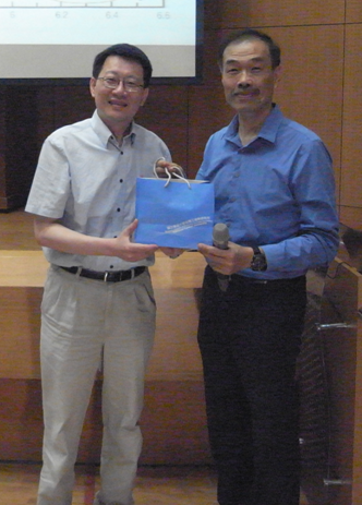
Chairman
Simon Chen visited GIPO at the invitation of GIPO professor Lung-Han Peng on June 9
(Fri.) and delivered a speech concerning “Semiconductor Lasers & Detectors and Their Applications in Optical Communication” at auditorium 101, Barry Lam
Hall. His speech was excellent and informative, and the
chairman
interacted very well with students. GIPO teachers and students learned a great deal from the event. |
| |
|
 |
|
Chairman Simon Chen (right), and Professor Gong-Ru Lin, chairman of GIPO (left) |
|
|
Time: |
4:30 pm, June 16 (Fri.), 2017 |
|
Speaker: |
Dr. Juen-Kai Wang, Research Fellow, Center for
Condensed Matter Sciences, NTU |
|
Topic:
|
From Femto to Nano and From Fundamental to Applications: My Optical Path |
|
|
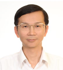
Dr. Juen-Kai Wang visited GIPO on June 16
(Fri.) and delivered a speech concerning “From Femto to Nano and From Fundamental to Applications: My Optical Path” at auditorium 101, Barry Lam
Hall. His speech was fascinating, and Dr. Wang interacted well with students. GIPO teachers and students all gained a great deal from the event. |
|
|
|
 |
|
Dr. Juen-Kai Wang, the speaker |
|
|
|
|
~ Sidelights on the
GIPO Cup sports games, 2017 ~ |
|
(Time: May 21, 2017; Location: NTU
Gymnasium) |
|
Compiled by Jui-Hsiang
Tsai, the president of GIPO Student
Association |
|
It is time for the once-a-year Photonics & Optoelectronics Cup Games again, sponsored by GIPO student association. Exercising, undoubtedly, is very good for everyone’s health. These games
are designed to remind GIPO students to exercise from time to time after completing their lab work and thereby improve their health and ease the pressure of studying. Aside from learning fast and studying hard, GIPO students apparently are also good in physical training. Many students do very well in several types of sports when they finish with experiments and are out on the fields. This year all the games ran smoothly. We would therefore like to thank all students for your enthusiastic participation and thank our association buddies for your hard work, which together, made this year’s games a success.
We were so lucky to have good weather on the day of the games, which allowed our contestants to come to the Gym without worry. We chose NTU Gymnasium to hold this year’s activities because we believe it is a nice place for our contestants to compete for medals. The games include three parts, i.e. badminton double, basketball 3 vs. 3 bullfight, and basketball funny contest. These three games are all very exciting and participants all showed excellent sportsmanship, regardless of whether they won or lost their games. At the end, contestants all enjoyed the event very much.
 |
|
Badminton preliminary contest |
 |
|
Badminton finals |
 |
|
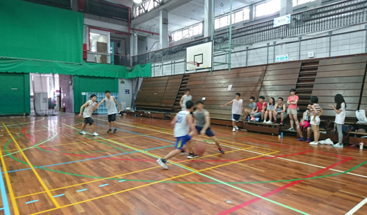
Basketball 3 vs. 3 bullfight |
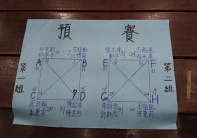
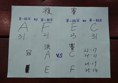
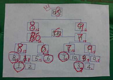
There were altogether 8 teams competing in the badminton double. After a preliminary contest, 4 teams entered the semi-final. And, after the semi-final, 3 winning teams came out on top in the final. All badminton players enjoyed the game very much. There were 10 teams competing in the basketball 3 vs. 3 bullfight game. During the play, the exciting hustle and bustle of the players made audiences nervous. Nevertheless, the players maintained their good manners throughout the game and nothing serious really happened. After 2 hours of fierce fighting, the 3 winning teams came out on top. By that time, these bullfight players were all exhausted, since the competition already consumed most of their energy. Then, we had a half-hour intermission for the players to have water and some rest. Next, we had the funny basketball contest, which was elaborately designed by our association buddies. After detailed instructions and a demonstration, each team took turns to play the game. During the play, some players just could not control their basketball and eventually lost it when they were trying to dribble it fast, and some even moved to wrong places, which attracted lots of laughter. It is a funny game. And it released the pressure and excitement from competition in previous badminton and basketball games. The contest achieved its designated purpose of bringing amusement to the audience.
 |
|
A snapshot of the basketball contest |
 |
|
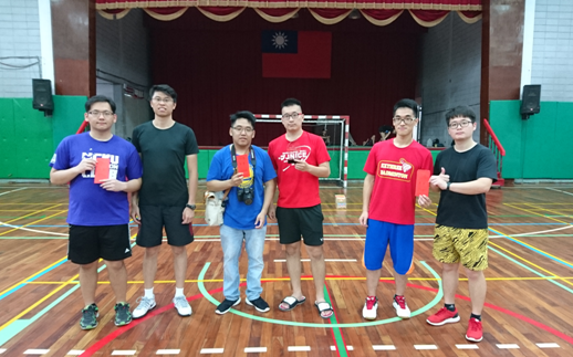
The 3 badminton winning teams |
 |
|
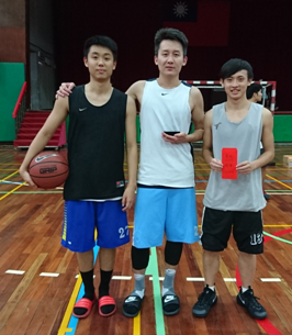
The basketball champion team |
After the funny basketball contest, this year’s games came to a close. We then awarded the winners with prizes and trophies. Everyone enjoyed a wonderful day and the games ended smoothly. We would encourage every GIPO students to participate in our future activities often and are looking forward to seeing you soon in the next event! Thanks everyone.
|
|
|
|
|
|
| |
|
|
|
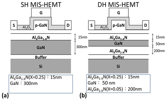
Suppression of Current Collapse in Enhancement Mode GaN based HEMTs using an AlGaN/GaN/AlGaN Double Heterostructure
Professor Jian-Jang Huang's laboratory
Graduate Institute of Photonics and
Optoelectronics, National Taiwan University
In this work, an AlGaN/GaN/AlGaN double heterostructure (DH) was proposed and demonstrated for enhancement mode operations. The DH MIS-HEMT possesses a higher threshold voltage and lower drain current under the same bias than the SH (single heterostructure) MIS-HEMT. Current collapse measurement shows superior properties of DH MIS-HEMT in long and short pulse measurement. The suppression of current collapse is mainly attributed to the raise of conduction band in the 2DEG channel, resulting in better electron confinement but less total electron density. The results indicate the potential of using the p-GaN/AlGaN/GaN/AlGaN E-mode HEMT structure for power device/system applications.
|
 |
|
Fig. 1. Device structures of the (a) SH MIS-HEMT and (b) DH MIS-HEMT. |
|
 |
|
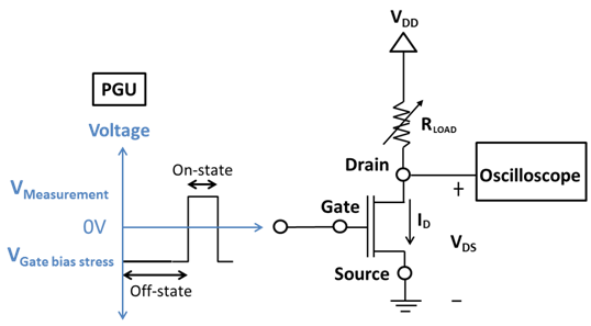
Fig. 2. Illustration of dynamic measurement setup. Vmeasurement is 4V at the on-state. |
|
 |
|
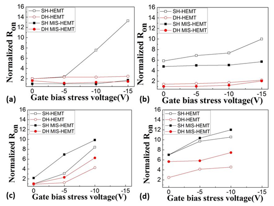
Fig. 3. Normalized dynamic on resistance of the devices stressed in (a) long pulse mode with VDD = 10V, (b) long pulse mode with VDD = 40V, (c) short pulse mode with VDD = 10V and (d) short pulse mode with VDD = 40V. Note that the RON is normalized to the channel resistance of the devices with nearly no stress (VDD=5V and VG=0V). |
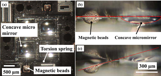
Magnetically Driven MEMS Cat’s Eye Array
Professor Jui-che Tsai
Graduate Institute of Photonics and Optoelectronics, National Taiwan University
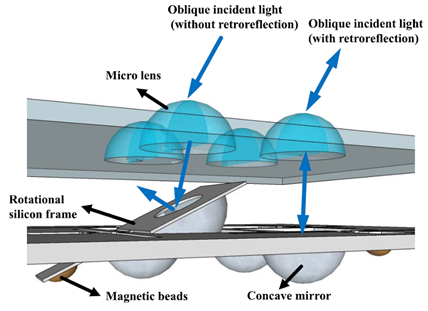
We have developed a micro-electro-mechanical system tunable cat’s eye retroreflector array for optical identification. A rotational concave mirror is employed in the retroreflector to achieve modulability of the retroreflected optical intensity (Fig. 1). The magnetic force between the permanent magnet and magnetic beads on the rotatable concave mirror unit enables magnetic actuation and accomplishes modulation (Fig. 2). The magnetically actuated mirror achieves a large tilt angle. The tilt angle of the concave mirror can change from 0° to 12°, with the retroreflection efficiency varying from 19% to 5% correspondingly. The retroreflection efficiency versus the position of the permanent magnet is characterized. A dynamic image can be generated by applying magnetic force individually to each cat’s eye in the array.
|
 |
|
Figure 1 |
|
 |
|
Figure 2 |
© 2016 IEEE
C. C. Chang, T. Y. Chen, and J. C. Tsai, “Magnetically driven MEMS
cat’s eye array as an optical identification,”
IEEE Photonics Technology Letters,
Vol. 28, No. 5, pp. 554-556, Mar. 2016
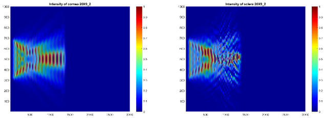
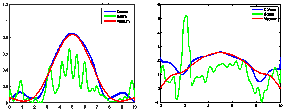
Simulation analysis of the cornea transparency
Professor Snow H. Tseng
Graduate Institute of Photonics and Optoelectronics, National Taiwan University
To analyze the transparency of cornea, we model monochromatic light propagation through a macroscopic scattering medium by employing the pseudospectral time-domain (PSTD) simulation technique. The geometric structure of cornea and sclera are modeled by different sizes and arrangements of the non-absorbing collagen fibrils, repsecitvely. Various factors are investigated, including wavelength of incident light, thickness of the scattering media, position of the collagen fibrils, and size distribution of the fibrils. The reported analysis provides information that may contribute to the understanding of the cornea transparency.
|
 |
|
Fig 1. (a) Light propagation through cornea-like structure. (b) Light propagation through sclera-like structure. |
|
 |
|
Fig 2. Comparison of the light amplitude and intensity propagating through cornea-like and sclera-like geometric structure. The x-axis is the cross-sectional width (μm). (a) Intensity distribution. (b) Phase distribution. |
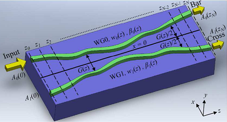
Broadband optical waveguide couplers with arbitrary coupling ratios designed using a genetic algorithm
Professor Ding-Wei Huang
Graduate Institute of Photonics and Optoelectronics, National Taiwan University
In this work, we present a generalized design of broadband optical waveguide couplers with arbitrary coupling ratios on the silicon-on-insulator platform. The device is segmented into 34 short sections, where the propagation constant and the coupling coefficient of each section are viewed as variables during the optimization process. The optimal variable combination is determined by a genetic algorithm. We can achieve a performance superior to that of other design methods with fewer degrees of freedom. For 75%/25%, 50%/50%, 25%/75%, and 0%/100% couplers, the device lengths are 34 μm and the ±2% bandwidths are all in excess of 100 nm at the central wavelength of 1580 nm.
Po-Han Fu, Yi-Chou Tu,
and Ding-Wei Huang* (2016, Dec.),
“Broadband optical waveguide couplers
with arbitrary coupling ratios designed
using a genetic algorithm,”
Optics Express,
24
(26), pp.30547-30561. (SCI)
|
 |
|
Fig. 1. Schematic of the broadband optical waveguide coupler. |
|
 |
|
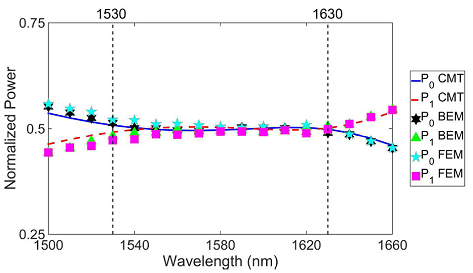
Fig. 2. Output power versus wavelength for
λ = 1500 – 1660 nm calculated by the CMT, BEM and FEM. |
Mechanical Bending Effect on the Performance of Flexible Complementary Oxide-TFT-Based Circuits Employing n-ZnO and p-SnO TFTs
Professor I-Chun Cheng
Graduate Institute of Photonics and
Optoelectronics, National Taiwan University
Complementary thin-film transistor (TFT) circuitry
consisting of inverters is the building block for realizing integrated logic
circuits on large-area and/or flexible substrates. Although numerous oxide-TFT
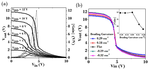
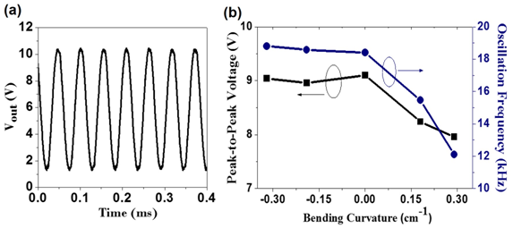
circuits have been reported previously, most of them were based on n-channel MOSFET (NMOS) technology. Here, we report flexible fully oxide-based complementary metal–oxide–semiconductor (CMOS) inverters and ring oscillators by the monolithic integration of flexible n-channel zinc oxide (ZnO) and p-channel tin monoxide (SnO) thin-film transistors (TFTs) on polyimide substrates. The TFTs have an inverted-staggered bottom-gated structure and were fabricated by a low-temperature rf-sputtering technique. The static voltage gain of a flexible oxide-TFT-based CMOS inverter with a geometric aspect ratio of 5 is ~12 at a supplied voltage (VDD) of 12 V. An oscillation frequency of ~18.4 kHz is obtained from a five-stage flexible oxide-TFT-based CMOS voltage control ring oscillator at VDD of 12 V. The mechanical bending effect on the electrical performance of the on-foil devices and circuits is then investigated by mechanical bending tests. The results show that the static voltage gain of the CMOS inverter and the peak-to-peak voltage and oscillation frequency of the ring oscillator decrease as the outward bending curvature (tensile strain) increases, while the influence of the inward bending curvature mechanical (compressive strain) is negligible.
|
 |
|
Fig. 1. (a) Static voltage transfer characteristics and voltage gain curves at different supplied voltages of the flexible oxide-TFT-based CMOS inverter. (b) Static voltage transfer characteristics of the CMOS inverter operated at VDD = 12 V under various bending levels. Inset: The static gain value of the CMOS inverter as a function of bending curvature. |
|
 |
|
Fig. 2. (a) Output waveform of a five-stage flexible CMOS ring oscillator. (b) Oscillation frequency and peak-to-peak voltage value as a function of bending curvature. |
Application of localization landscape theory of disorder in semiconductors. Application to carrier localization, absorption, transport and recombination in light emitting diodes
Professor Yuh-Renn Wu's laboratory
Graduate Institute of Photonics and
Optoelectronics, National Taiwan University
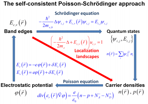
This work was the collaboration work with France team in Ecole polytechnique in Paris and UCSB SSLEC in united states under the support of Taiwan-ANR collaboration project. The goal is to directly apply the localization landscape theory into the simulation program in order to achieve an efficiency way for obtaining the effective quantum potential. In the first PRB paper, we try to prove that by solving the localization landscape u to obtain the effective quantum potential 1/u, we can bypass the time consuming process of solving Schrodinger equation eigen value problems.
|
 |
|
Fig. 1. Schematic structure of the self-consistent Poissonlandscape model allowing us to bypass solving the Schrödinger equation. [1] |
|
 |
|
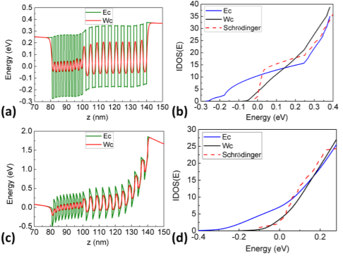
Fig. 2. (a), (c) The conduction band potential (Ec) and effective quantum confining potential (Wc) for
m-plane (top) and c-plane (bottom) double-period SLs. (b), (d) The corresponding integrated density of states (IDOS). [2] |
As shown in Fig.2, by solving the localization landscape, we can obtained the effective quantum potential wn in red line in Fig. 2(a) and 2(c). By applying the distribution of quantum potential to obtain the integrated density of states, it would be close to the result of Schrodinger eigen solver. However, the speed is a few order faster.
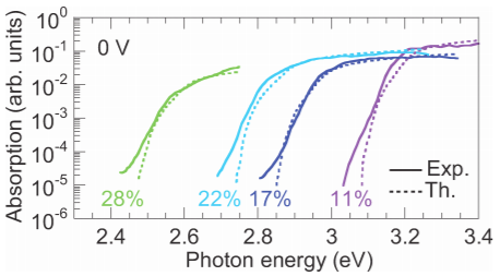
In the second paper, we try to apply the landscape theory in the 3D modeling to explain the Urbach tails in semiconductors related to compositional disorder. The Urbach tail observed in InGaN alloy quantum wells of solar cells and LEDs by biased photocurrent spectroscopy is shown to be characteristic of the ternary alloy disorder. The broadening of the absorption edge observed for quantum wells emitting from violet to green (indium content ranging from 0% to 28%) corresponds to a typical Urbach energy of 20 meV. Our 3D model is used for obstaining the effective potential in disorder. This model incorporating compositional disorder accounts well for the experimental broadening of the Urbach tail of the absorption edge. For energies below the Urbach tail of the InGaN quantum wells, type-II well-to-barrier transitions are observed and modeled. This contribution to the below-band-gap absorption is particularly efficient in near-ultraviolet emitting quantum wells. When reverse biasing the device, the well-to-barrier below-band-gap absorption exhibits a red-shift, while the Urbach tail corresponding to the absorption within the quantum wells is blue-shifted, due to the partial compensation of the internal piezoelectric fields by the external bias. The good agreement between the measured Urbach tail and its modeling by the localization theory demonstrates the applicability of the latter to compositional disorder effects in nitride semiconductors.
|
 |
|
Fig. 3. Absorption curves for InGaN/GaN
structures of different indium
composition at 0 V computed using the 3D
theoretical model incorporating
compositional disorder and QW electric
field as a function of different
smoothing parameters (dashed line). The
responsivity curves measured by BPCS of
InGaN/GaN solar cells of different
indium composition at 0 V are also shown
(continuous lines). [2] |
In the third paper, we finally apply this model in studying the carrier transport and recombination. We provide a novel method to account for quantum disorder effects into the classical drift-diffusion model of semiconductor transport through the localization landscape theory. Quantum confinement and quantum tunneling in the disordered system change dramatically the energy barriers acting on the perpendicular transport of heterostructures. In addition, they lead to percolative transport through paths of minimal energy in the two-dimensional (2D) landscape of disordered energies of multiple 2D quantum wells. This model solves the carrier dynamics with quantum effects self-consistently and provides a computationally much faster solver when compared with the Schrödinger equation resolution. The theory also provides a good approximation to the density of states for the disordered system over the full range of energies required to account for transport at room temperature. The current-voltage characteristics modeled by three-dimensional simulation of a full nitride-based light emitting diode (LED) structure with compositional material fluctuations closely match the experimental behavior of high-quality blue LEDs. The model allows also a fine analysis of the quantum effects involved in carrier transport through such complex heterostructures. Finally, details of carrier population and recombination in the different quantum wells are given.
|
 |
|
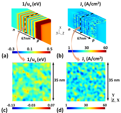
Fig. 4. (a), (b) The perspective views along the
z direction of vertical transport of the 1/ue and z component of current (Jz), respectively. (c), (d) The 1/ue and Jz value in the midplane (x-y plane) of the third QW. All figures are solved by 1/u-Poisson-DD model, where the LED current density is 20 A.cm-2. |
All
these simulation tools are shared at http://yrwu-wk.ee.ntu.edu.tw,
where users in academics can download for
usages.
References:
1. Marcel Filoche, Marco Piccardo, Yuh-Renn Wu,
Chi-Kang Li, Claude Weisbuch, and Svitlana
Mayboroda, "Localization landscape theory of
disorder in semiconductors I: Theory and
modeling", Phys. Rev. B, 95, 144204, April,
2017. DOI:
10.1103/PhysRevB.95.144204
2.
Marco Piccardo, Chi-Kang Li, Yuh-Renn Wu, James
S. Speck, Bastien Bonef, Bob Farrell, Marcel
Filoche, Lucio Martinelli, Jacques Peretti, and
Claude Weisbuch, "Localization landscape theory
of disorder in semiconductors II: Urbach tails
of disordered quantum well layer", Phys. Rev. B,
95, 144205, April, 2017. DOI:
10.1103/PhysRevB.95.144205
3.
Chi-Kang Li, Marco Piccardo, Li-Shuo Lu,
Svitlana Mayboroda, Lucio Martinelli, Jacques
Peretti, James S. Speck, Claude Weisbuch, Marcel
Filoche, and Yuh-Renn Wu *, "Localization
landscape theory of disorder in semiconductors
III: Application to transport and radiative
recombination in light emitting diodes.", Phys.
Rev. B, 95, 144206, April, 2017. DOI:
10.1103/PhysRevB.95.144206
|
|
|
|
|
|
|
| |
|
|
 |
|
 |
|
|
|