|
August 2016 - October 2016 |
| |
|
|
 |
|
 |
| |
Publisher: Chairman Gong-Ru Lin Editors: Professor
Chao-Hsin Wu, Ms. Hsiao-wen Lin January 15, 2017 |
| |
|
 |
|
Congratulations! GIPO professor Jian-Jang Huang receives the title of "2017 OSA Fellow".
Congratulations to the following graduate students on being awarded, under the instruction of Professor Gong-Ru Lin, the “2016 Youth Theses Prize of the Chinese Institute of Electrical Engineering”. The winners’ list is as follows:
The 1st place:
|
Winner |
Adviser |
Thesis title |
|
Tsai-Chen Wu (master student) |
Professor Gong-Ru Lin |
Laser diode based free-space, underwater, and white-lighting visible light communication |
The 3rd place:
|
Winner |
Adviser |
Thesis title |
|
Cheng-Hsuan Hsieh (master student) |
Professor Gong-Ru Lin |
All-optical switching in C-rich SiCx waveguide based on nonlinear Kerr and SPM effects |
|
|
 |
|
 |
|
| |
|
|
|
~ Sidelights on the 2016 GIPO undergraduates’ optoelectronics summer camp ~
(August 12~14, 2016, at Barry Lam Hall, NTU)
Compiled by
Yu-Ting Huang
(the president of GIPO Student
Association) and
Way-Yu Chen
(the convener)
Aside from focusing on academic studies and students’ well-being, GIPO, NTU, also extends its attention to undergraduate students who are interested in joining us. Therefore, we hold a GIPO undergraduates’ optoelectronics summer camp every year, usually lasting 3 days, from morning till evening. The event includes all meals, transportation and, of course, classroom studies. This camp is especially designed for the 3rd and 4th grades undergraduates. Its purpose is to introduce photonics and optoelectronics, the general situation of GIPO, and related information concerning GIPO admission applications. As a result, it provides a valuable experience and opportunity for interested students.
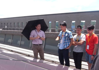
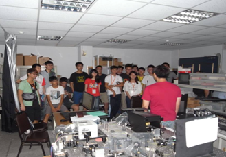
On the morning of the 1st day, students listened to several professors’ speeches, and then, Professor Chao-Hsin Wu led students to visit the solar energy plates on the roof of Barry Lam Hall. We were very grateful that he took the time to pass on valuable knowledge in the heat. In the afternoon, after a delicious lunch, we visited several photonics laboratories. It was amazing to listen and watch graduate students explaining the usage of laboratory instruments and experiment principles. Graduate students in Professor Hoang-Yan Lin’s laboratory were particularly helpful, showing visitors the application of holography, which has combined technology with film, making students even more interested in studying photonics and optoelectronics.
|
 |
 |
|
Professor Chao-Hsin Wu (1st left). He is well-known as the GIPO Yu-Yen Peng, a handsome Taiwanese actor. |
Laboratories visiting |
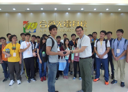
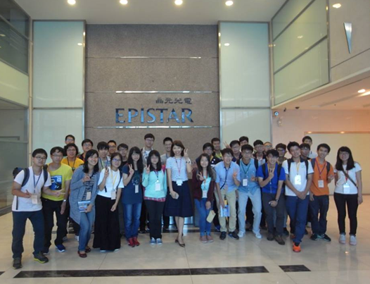
On the 2nd day, we visited H.P.B. Optoelectronics Co., Ltd. in Taichung and Epistar Corporation’s Tzunan factory. At H.P.B., they let us visit several manufacturing rooms, and gave us a detailed introduction of their company’s history. We were also allowed to try out operating a car using hand gestures, and H.P.B. thoughtfully provided us with snacks, soft drinks and boxed meals. H.P.B. is certainly an excellent corporation which welcomes students seeking employment after graduation. In the afternoon, we visited Epistar Corporation. They received us in their meeting room, gave us a detailed introduction of their company, and provided us with snacks. Although they did not arranged for us to visit their manufacturing rooms, the receiving staff members were all very nice and cordial.
|
 |
|
Way-Yu Chen (front left), GIPO graduate student, convener of this summer camp |
|
 |
|
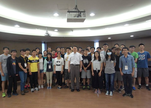
A group photo of all attendants |
On the morning of the 3rd day, after listening to a wonderful speech from a professor, we then had a highly-anticipated session of hands-on experiments. We made some practical holograms and illusion dinosaurs. With guidance from the staff we used transparent projecting films to make simple, small projectors, and used them to display 3D images. The illusion dinosaur experiment is obtained from the internet. It folds a sheet of paper into a dinosaur, and produces an illusion where the dinosaur appears to be starting at you, no matter how you turn your head, which is certainly very scary. These two experiments were highly appreciated by the undergraduate students. They discussed it enthusiastically during experiments, giving us affirmation for our hard work in designing these experiments.
After a delicious lunch, students then had their last classroom lesson. And, following that last lesson, we came to the important moment of awarding certificates. After a brief address, the GIPO chairman, with the help of student association staff members, awarded a certificate and a souvenir to every student. We believe they will undoubtedly tell their classmates about the camp when they return to their own universities. We, the GIPO student association staff, felt very relaxed after the camp’s smooth successful conclusion. We also believe that the wonderful memories of these three days will stay in our minds forever.
|
 |
|
A group photo of GIPO chairman, working staff members and all students |
|
|
|
|
|
|
|
| |
|
|
|
Regularly-patterned Multi-section GaN Nanorod Arrays Grown with a Pulsed Growth Technique
Professor C. C. (Chih-Chung) Yang
Graduate Institute of Photonics and
Optoelectronics, National Taiwan
University
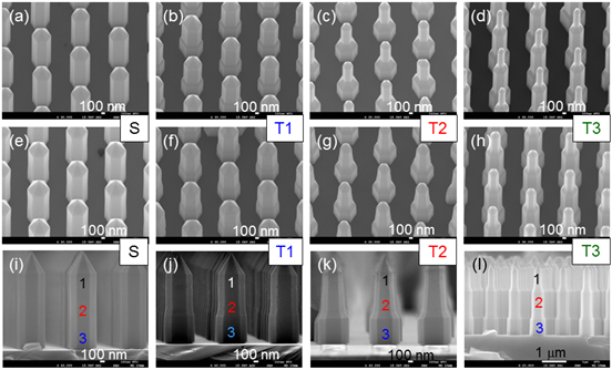
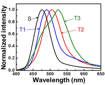
The growth of regularly-patterned multi-section GaN nanorod (NR) arrays based on a pulsed growth technique with metalorganic chemical vapor deposition is demonstrated. Such an NR with multiple sections of different cross-sectional sizes is formed by tapering a uniform cross section to another through the decrease of Ga supply duration stepwise for reducing the size of the catalytic Ga droplet. Contrast line structures are observed in either a scanning electron microscopy or a transmission electron microscopy image of an NR. Such a contrast line-marker corresponds to a thin Ga-rich layer formed at the beginning of GaN precipitation of a pulsed-growth cycle and illustrates the boundary between two successive growth cycles in pulsed growth. By analyzing the geometry variation of the contrast line-markers, the morphology evolution in the growth of a multi-section NR, including a tapering process, can be traced. Such a morphology variation is controlled by the size of the catalytic Ga droplet and its coverage range on the slant facets at the top of an NR. The comparison of emission spectrum between single-, two-, and three-section GaN NRs with sidewall InGaN/GaN quantum wells (QWs) indicates that a multi-section NR can lead to a significantly broader sidewall emission spectrum.
|
|
|
Fig. 1 (a)-(d): Tilted SEM images of a single-section (sample S), two 2-section (samples T1 and T2), and one 3-section (sample T3) n-GaN NR arrays. (e)-(h): Tilted SEM images after three periods of InGaN/GaN QWs are grown on the sidewalls of the n-GaN NRs in samples S and T1-T3, respectively. (i)-(l): Cross-sectional SEM images of the QW NR arrays in samples S and T1-T3, respectively. Numbers 1-3 are marked for indicating the locations of local cathodoluminescence measurements. |
|
|
|
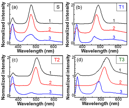
Fig. 2 (a)-(d): Local cathodoluminescence spectra at the three locations for samples S and T1-T3, respectively. |
|
|
|
Fig. 3 Normalized photoluminescence spectra of the QW NR arrays in samples S and T1-T3. |
Coupling Behaviors of a Radiating Dipole with the Surface Plasmon Induced on a Metal Protrusion
Professor Y.
W. Kiang’s Laboratory
Graduate Institute of Photonics and
Optoelectronics, National Taiwan
University
The coupling behaviors of a radiating dipole with
localized surface plasmon (LSP) resonance modes induced on an Ag protrusion in a
GaN layer are numerically studied with an algorithm including the feedback
effect of LSP resonance to modify the emission behavior of the radiating dipole.
Two spectral ranges (400 – 570 and 570 – 800 nm) of radiated power enhancement
can be observed. The radiated power enhancement in the long-wavelength
(short-wavelength) range is generated through the coupling of the radiating
dipole with the dipole and quadrupole (higher-order) LSP resonance modes induced
on the protrusion. Because the LSP electromagnetic fields of those higher-order
modes are mainly distributed around the tip of the protrusion, which is close to
the radiating dipole, the radiated power enhancement is quite effective in the
blue-green range even though the corresponding metal absorption can be higher
than that of a lower-order LSP mode. Compared with the configurations of surface
metal nanoparticle (NP) and embedded metal NP, the protrusion structure has the
advantages of relatively higher radiated power enhancement in the blue-green
spectral range and relatively lower fabrication cost from a practical
application viewpoint.
|
|
|
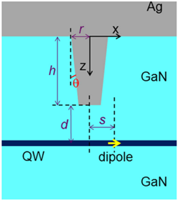
Fig. 1. Problem geometry of numerical simulation. A truncated-cone-shaped Ag protrusion with the base radius r, height h, and inclination angle θ in GaN is connected to the upper half-space of Ag. The vertical distance between the protrusion tip and the designated QW, which consists of a radiating dipole array in the x-y plane, is d. The lateral position of a radiating dipole is defined as s. |
|
|
|
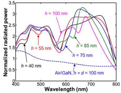
Fig. 2. Normalized radiated powers as functions of wavelength by fixing the distance between the protrusion tip and the radiating dipole, d, at 30 nm and varying the protrusion length, h. The lateral distance of the radiating dipole s is set at s=0. The radiating dipole is oriented along the x-axis. The dashed curve is plotted for the normalized total radiated power of a radiating dipole located in GaN 100 nm away from an air/GaN interface. |
MBE growth of the highly mismatched alloy InAsPSb
Professor Hao-Hsiung Lin
Graduate Institute of Photonics and
Optoelectronics, National Taiwan
University
Because of the strong internal bond distortion resulting from highly mismatched bond lengths, the InPSb and InAsPSb alloys are with a lot of peculiar properties which have not been fully understood yet. We used VG V80H GSMBE to grow the two alloys on InAs and GaAs. Also, with the surprising property that the lattice constant of InAsPSb remains approximately equal to that of InAs, we can treat the quaternary alloy as a buffer layer between GaAs and InAs. Results show that the buffer layer is feasible, although there are some stacking faults in the interface.
|
|
|
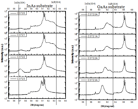
Fig. 1. XRD of InPSb grown on InAs and GaAs substrates. C3723 shows a sharp and narrow-line width epilayer signal without phase separation. |
|
|
|
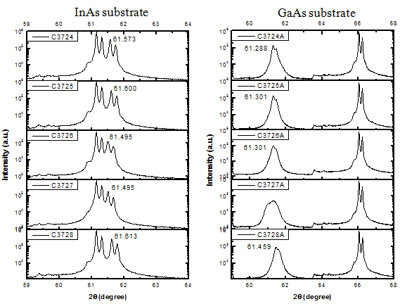
Fig. 2. XRD of InAsPSb grown on InAs and GaAs substrates. No matter how the composition changes, the diffraction angles of InAsPSb keep approximately equal. |
|
|
|
 |
|
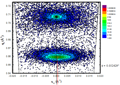
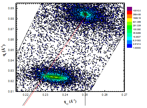
Fig. 3. (004) and (115) RSM of InAs/InAsPSb/GaAs structure. |
|
|
|
Fig. 4. HRTEM cross-section view of InAs/InAsPSb/GaAs structure. |
High Efficient Planar Heterojunction Perovskite Solar Cells via Sandwich Evaporation Technique
Professor Ching-Fuh Lin’s laboratory
Graduate Institute of Photonics and
Optoelectronics, National Taiwan University
Due to the gradual depletion of fossil fuels, the energy issue has received wide attention in this century. The world is making many efforts to develop alternative energy. Solar energy is an inexhaustible and readily available resources on earth. On the top of that, it is eco-friendly to our environment. For these advantages, the development of solar cells has become an excellent strategy to solve the shortage of energy. Among many types of solar cells, perovskite solar cells suddenly appear on the horizon and the conversion efficiency has been made significant progress from 3% to above 20% in just six years.
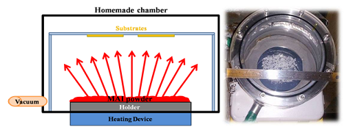
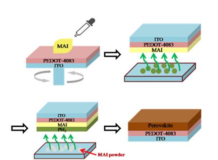
Although high-efficiency perovskite solar cells have been achieved, perovskite formed by solution process, in general, is very susceptible to the atmosphere and moisture. The perovskite grains usually become small and messy by the rapid formation of perovskite. In this research, we developed a new method using a homemade chamber, called Sandwich Evaporation Technique (SET), to form the perovskite layer, as shown in Fig.1. The process can be mostly conducted in the atmosphere and not be affected by the environment easily. The process includes the following steps. First, we raised a sandwich-like structure, MAI/PbI2/MAI, to fabricate the active layer of perovskite to enhance the current density, as shown in Fig. 2. Second, the perovskite solar cells are fabricated with the traditional structure of ITO/PEDOT-4083/Perovskite/PCBM/PEI/Ag, which can successfully achieve the power conversion efficiency of 14.03%.
|
|
|
Fig. 1. The picture of the homemade chamber of Sandwich Evaporation Technique (SET) process. |
|
 |
|
Fig. 2. The picture of Sandwich Evaporation Technique (SET) process. |
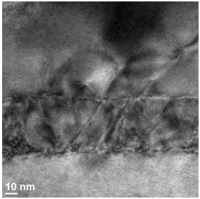
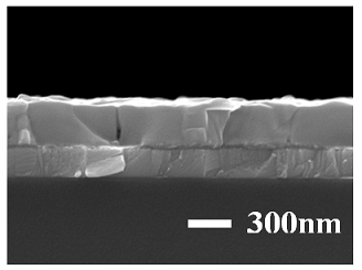
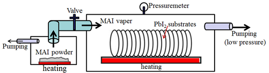
Furthermore, we modify those techniques that can make the better film of the active layer. IPA, CB have been applied on the substrates to slow down the reaction. Here this mechanism is refined for the SET process. Vials with solvent are placed inside the chamber directly. With the refined process, we are able to achieve 14.62% of perovskite solar cells with a higher current density and large crystals of perovskite, as shown in Fig. 3. This brand new method to fabricate the perovskie under atmosphere environment could potentially enable the mass production in the future using the Sandwich Evaporation Technique (SET), as shown in Fig.4.
|
|
|
Fig. 3. The SEM image of the perovskite. |
|
 |
|
Fig. 4. The schematic diagram of the Sandwich Evaporation Technique (SET). |
Improved Internal-Quantum Efficiency of GaN-Based LEDs
Professor Chieh-Hsiung Kuan
Graduate Institute of Photonics and
Optoelectronics, National Taiwan
University
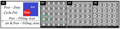
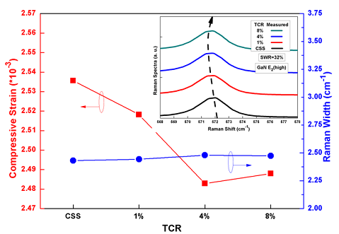
Instead of the limited exposure feature sizes of conventional photolithography, the ELIONIX ELS-7000 E-beam lithography system and the wet-etching technology were conducted to carry out the investigation. All patterned-sapphire substrates (PSSs) were all arranged in squares with the period of 2000nm and with various post-duty cycles (PDCs) of 1, 4 and 8%, which is defined in Fig. 1(a), respectively. Each square had a hexagonal post. SEM images of accomplished PSSs are shown in Fig. 1(b)-(d). The PSSs and a conventional sapphire substrate (CSS) with polished surface were grown using low pressure metal organic chemical vapor deposition (LP-MOCVD). The light-emitting diodes (LEDs) were encapsulated with TO-46 metal can package with a chip size of 17×34 mil2.
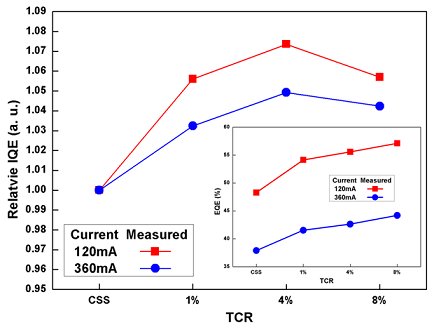
Figure 2 shows the residual compressive strain and the associated Raman width of the GaN-based PSS LEDs. With the increase of PDC, the residual compressive strain of the GaN-based PSS LEDs reduces first and then slightly increases as compared to the sample with the CSS. Fig. 3 shows the relative IQE versus PDC of the GaN-based PSS LEDs biased at injection currents of 120mA and 360mA, respectively. With the increase of PDC in contrast to the CSS, the reduced residual compressive strain leads to the enhanced relative IQE under the same crystalline quality.
|
|
|
Fig. 1. The SEM images of different PSSs and the definition of post-duty cycle. |
|
 |
|
Fig. 2. The residual compressive strain with the associated Raman width. The inserted figure is the Raman spectra. |
|
 |
|
Fig. 3. The relative IQE of the LEDs, calculated from the inserted figure regarding the EQE versus PDC. |
|
|
|
|
|
|
|
| |
|
|
 |
|
 |
|
|
|