| |
|
Publisher:
Chairman Gong-Ru Lin Editors: Professor
Chao-Hsin Wu, Ms. Hsiao-wen
Lin December 30, 2013
|
| |
|
|
 |
|
Congratulations! GIPO Professor
Gong-Ru Lin receives
the title of "2014
OSA Fellow".
Congratulations to Professor Jr Hau He’s team on their successful research, and the publication of their research results in PIEEE, in “Fully transparent resistive memory employing graphene electrodes for eliminating undesired surface effects”. For more information, please refer to NTU website Campus Focus.
(http://www.ntu.edu.tw/spotlight/2013/130805_1.htm)
|
|
 |
|
 |
|
| |
|
|
|
|
|
October “Photonics
Forum” Highlights
(compiled by Li-Chi Yao) |
|
|
3:30 pm, Fri., Oct. 4th, 2013 |
|
Lecturer: |
Prof. Hsiung Chang
(Advance Photonics Center, Electronics and Engineering College, Southeast University) |
|
Topic:
|
MOCVD growth and fabrication process of high performance GaN-based LEDs |
| |
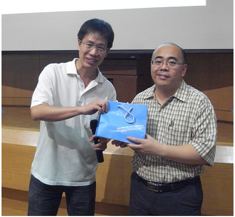
Prof. Hsiung Chang, in answer to Prof. Zhe-Chuan Feng’s invitation, visited GIPO on Oct. 4th
(Fri.) and delivered a speech concerning “MOCVD growth and fabrication process of high performance GaN-based LEDs”
at lecture theater
101, Barry Lam Hall. His speech was splendid and the professor interacted well with students. GIPO teachers and students participated in this activity enthusiastically and benefitted a great deal.
|
| |
|
 |
|
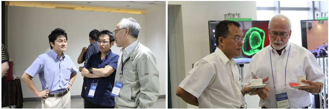
Prof. Hsiung
Chang
(right) and
Prof. Snow
H. Tseng
(left), the
host of the
speech |
|
|
|
|
|
3:30 pm, Fri., Oct. 18th, 2013 |
|
Speaker: |
Prof. Hao-Chung Kuo
(Distinguished Professor, Institute of Electro-optical Engineering, NCTU) |
|
Topic:
|
Recent progress of efficiency droop improvement for high efficiency GaN-based light-emitting diodes |
| |
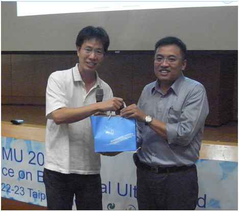
Prof. Hao-Chung Kuo visited GIPO on Oct. 18th
(Fri.) and delivered a speech concerning “Recent progress of efficiency droop improvement for high efficiency GaN-based light-emitting diodes” at
lecture theater 101, Barry Lam Hall. His speech was marvelous and the professor interacted very well with students. GIPO teachers and students learned a great deal from the experience.
|
| |
|
|
|
Prof. Hao-Chung Kuo
(right) and
Prof. Snow
H. Tseng
(left), the
host of the
speech |
|
~
A self introduction of the president of GIPO Student Association, 2013 academic year ~
 Hi, GIPO teachers and students, I’m Ting-Hao Chen, the president of GIPO Student Association, 2013 academic year. I’m very happy and honored to be the president and to have this opportunity to serve you. Hi, GIPO teachers and students, I’m Ting-Hao Chen, the president of GIPO Student Association, 2013 academic year. I’m very happy and honored to be the president and to have this opportunity to serve you.
Regarding student associations, I’m of the opinion that there is a slight difference between graduate school student associations and undergraduate student associations. In graduate schools, students study in different laboratories; each laboratory forms an independent unit. Even though there are 100 GIPO students every year, not many students will know each other even after graduation. GIPO students seem destined to be divided into different units; therefore, it is the most important job for this association to break these units limitation, to increase interaction among all GIPO students. We have been striving to strengthen bonds among students through activities such as lunch and dinner parties in the 1st semester and ball games in the 2nd semester. We sincerely hope that GIPO can become more of a big, joyful family, and that is exactly what I am striving for during my term as well.
Time goes by quickly. I remember that I joined the student association because I wished to make more friends, not just classmates of the same laboratory, but students of all other laboratories. After getting involved in several association activities, I believe that I have made the perfect decision in joining GIPO student association. Students of this association are very outstanding because they carry out missions quickly and efficiently. Every time we see GIPO students having a great time, we feel having done something worthwhile.
Nevertheless, there is still
a lot of room for us to
improve ourselves, and we
need more excellent students
to help us. Every GIPO new
student, or old student, is
welcome to join us. I
herewith, representing the
association, sincerely
invite you to join us. My
study room is located at
Min-Da hall, room 520; you
are welcome to drop in for a
chat anytime. Finally, I
would like to thank those
ladies in the GIPO office
for their kind assistance,
which has made our work
easier. I would also like to
thank my adviser, Chih-I Wu,
for his generous support.
And, I would like to thank
GIPO most of all for
bringing me such a wonderful
memory!
|
|
|
|
|
|
| |
|
|
|
|
|
~
BioPhotonics 2013 ~
(Time: July 17~19, 2013;
Location:
Barry Lam Hall, NTU)
Compiled by Chien-Chung Tsai,
Kuang-Yu Hsu, Chia-Kai Chang,
and Ya-Ting Hsu
The 2nd biophotonics conference was held at National Taiwan University during July 17~19, 2013, two years after the successful conclusion of the 1st conference at Parma University, Italy. On the morning of the 1st day, NTU president, Pan-Chyr Yang, presided over the opening ceremony. Afterward, during the theme speech session, Chung-Hsuan Chen, an Academia Sinica fellow, and Jürgen Popp, a professor of Jena University, Germany, spoke about the major applications of DNA mass spectrometer and Raman spectrometer respectively. Next on the agenda, were topics concerning micro-channel and biochips. A lunch featuring a Chinese and western combined buffet, was served in Barry Lam
Hall. Although space in the lunch room was limited, and the room was crowded with foreign and domestic scholars, the lack of space did provide an excellent opportunity for everyone to get to know each other, and exchange knowledge of different domains of biophotonics. In the afternoon, there were topics concerning optical coherence tomography and medical imaging. These topics included many types of imaging technologies which could, when used in different applications, create various imaging modes. Dinner in the evening of the 1st day was served at the Garden cafeteria of Howard Hotel. Those interested in the day’s topic stook this opportunity enter discussions with related scholars for further information, and thus created further exchange of knowledge among them.
In the morning of the 2nd day, participants proceeded to discuss the tissue imaging topic, which focused mostly on the mechanism of imaging-assisting-operation therapy. In medical nidus, surface imaging is no longer adequate, it needs to integrate 3D imaging to precisely locate, excise and sinter problem tissues. At 10:30
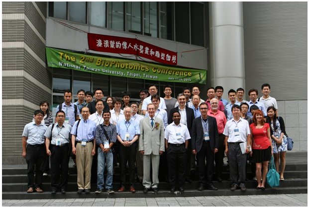
am, all conference participants assembled in
front of the gate of Barry Lam Hall to take a group photo, for a memorial of this conference. Next, there was the paper poster and digital poster session. Nowadays, some foreign conferences have increasingly developed facilities for digital poster sessions; in order to keep up with the multimedia era, to show participants’ research results more vividly, and to increase the adaptability of the agenda, we have also increased digital poster facilities for the conference. In the afternoon, the topic discussed was the application of fluorescence microscope. This topic has great relevance to cells and molecular biology, and was therefore, of great help to those who were studying cell imaging. The dinner on the 2nd day was served at Shin Yeh restaurant, located on the 85th floor of Taipei 101 tower, a landmark of Taipei. We had arrived at the restaurant before sundown, and the day was still clear. All the foreign and domestic scholars were immediately attracted by the view out of the restaurant window, the sundown by Guanyin mountain and Dansui river mouth, and street lights in the whole Taipei basin.
The agenda of the 3rd day morning was the sensing and components of molecular grades. The theme of this topic was to identify molecular structures or diseases by virtue of interactions among surface plasma wave, antigen and antibody. In the afternoon, there was the topic of applicable biomedical implements which could have great potential for the following ten years. After all papers had been presented, Prof. Selleri announced that the next biophotonics
conference would be held in Florence, Italy, the
birthplace of the Renaissance, at a location that looked like a European palace.
In order to help Taiwanese photonics professionals catch up with international biomedical applicable photonics technologies, we especially arranged 3 tutorials in the afternoon of July 16th. Professor Yu-Hwa Lo, UCSD,
Professor Chung-Ping Chen, UC Irvine, and Professor Chi-Kuang Sun, GIPO, NTU, delivered speeches concerning detailed theoretical analysis and experiment verification, and the most updated development and application information of cell micro-channel, optical coherence tomography and cell nonlinear imaging technologies. These tutorials were very beneficial for the photonics professionals who would soon be entering the study of biomedicine.
As we could see from their reports presented in the conference, there was a similarity among foreign professors’ research, i.e. they have been striving hard toward the goal of developing an intact set of technology, or instruments, and to certify them, such as with FDA certification, in due time. It could also be said that in peer reviews of foreign universities, the invention of some commercial instrument facilities, or the establishment of some high-tech corporation could be an index of their research success. This similarity could, perhaps, serve as a reference for Taiwanese academia.
We would like to thank Professor Si-Chen Lee, former president of NTU, for his service as the chairman of the counseling committee. Also we would like to thank Professor Sheng-Lung Huang, GIPO, NTU, and Professor Fu-Jen Kao, Institute of Biophotonics, National Yang-Ming University, for their efforts in preparing this conference, and thank
Yen Tjing Ling Industrial Research Institute, NTU, for their kind assistance. With their help, the participating scholars not only learned about international-level biophotonics technologies, but also gained an opportunity for international academic exchange and cooperation.
 |
|
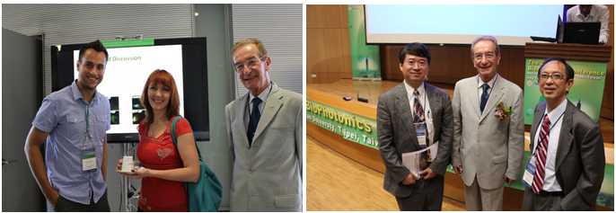
A group photo of the
participating scholars, in front of
Barry Lam Hall |
 |
 |
|
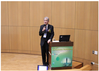
President Pan-Chyr Yang addressing the
conference at the opening ceremony |
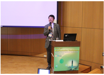
The conference chair, Professor Sheng-Lung
Huang, addressing the conference |
 |
|
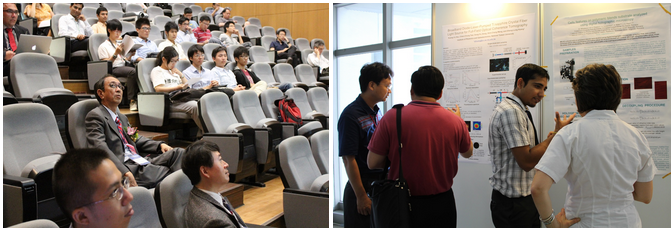
A snapshot of the
conference scene |
 |
|
A snapshot of the
conference scene |
 |
|
A snapshot of the
conference scene |
|
|
|
|
|
|
|
| |
|
|
|
|
|
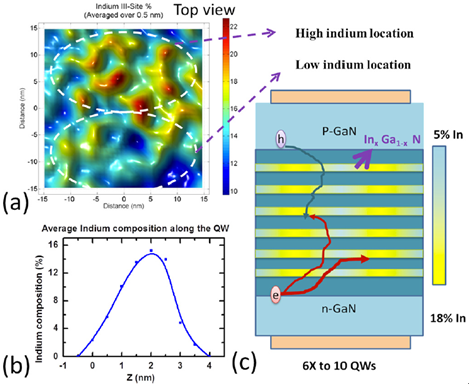
Analyzing the physical properties of InGaN multiple quantum well light emitting diodes from nano scale structure
Professor Yuh-Renn Wu
Graduate Institute of Photonics and
Optoelectronics, National Taiwan University
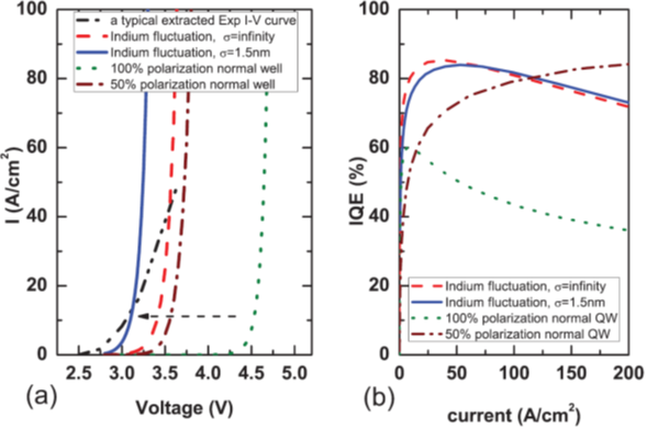
We reported on the influence of nanoscale indium fluctuations on physical properties for multiple quantum well (QW) light emitting diodes (LEDs). A commercial grade c-plane LED was analyzed by atom probe tomography, and the indium composition distribution was extracted. The influence of the degree of fluctuation and number of quantum wells were analyzed by a two-dimensional Poisson and drift-diffusion solver with very fine mesh and compared to the experimental result and a simple normal quantum well model. The studies show that the indium fluctuation will significantly impact the device’s internal quantum efficiency, droop behavior, and current-voltage curves. Including the influence of indium-fluctuation gives a better prediction of the device performance.
The simulation result shows that by considering the indium composition fluctuation in the QW, it is possible to explain the low forward voltage in the commercial blue LED diode. The influence of indium fluctuation to the IQE and carrier transport is very significant, which cannot be ignored in the device design and modeling. Of course, including the tunneling and ballistic transport with consideration of indium fluctuation will give the best prediction of device characteristics. In future work, direct results of indium fluctuation obtained from atom probe will be used as the input for our 3D Poisson, drift-diffusion, and k.p Schrodinger equation solver to analyze the emission spectrum and carrier transport characteristic and compare with experiments.
|
 |
|
Figure 1. (a) The top view of indium composition fluctuation in the lateral direction inside the MQW LED from atom probe measurement. (b) The average indium composition along the vertical direction of the QW from atom probe data. (c) The schematic of device structure to be modeled in this study. The QW thickness is 3 nm and the barrier thickness is 10 nm. The QW number is from 6 to 10 depending on different cases. |
|
 |
|
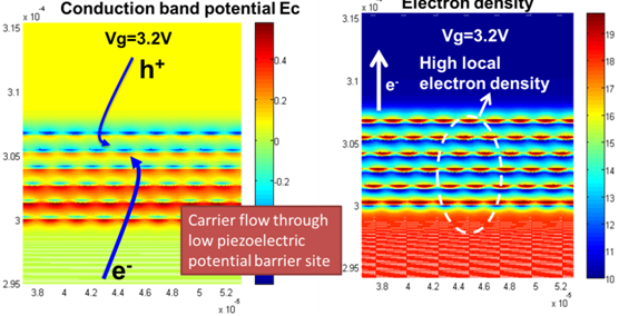
Figure 2. (a) The calculated potential distribution by assuming a fluctuation of indium composition in the QW. (b) The calculated electron density at 3V, which is near the forward voltage. |
|
 |
|
Figure 3. (a) The experimental and calculated I-V curve for the cases with indium fluctuation and without indium fluctuation. The extracted experimental I-V was from the average value of Nichia’s LED chip (see Refs. 20 and 21 in the original paper). (b) The calculated internal quantum efficiency under different simulation model. |
|
|
Research progress from Jr-Hau (JH) He's lab
Professor Jr-Hau He
Graduate Institute of Photonics and
Optoelectronics, National Taiwan University
Transparent memory
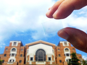
Transparent electronics is an emerging technology employing “invisible” electronic circuitry and optoelectronic devices, such as building-integrated photovoltaics and touch panel displays. In view of the integration toward see-through electronics, transparent non-volatile memory devices are indispensable and still deficient. Recently, in Jr-Hau He’s lab, they fabricated ZnO transparent resistance random access memory (TRRAM) devices employing atomic layered graphene at the surface of ZnO exhibiting not only excellent transparency (less than 2% absorptance by graphene) but also stable resistive switching characteristics. The obtained insights show guidelines not only for TRRAM device design and optimization against the undesired switching parameter variations but also for developing practically useful applications of graphene. The researcher presented their work in Proceeding of the IEEE. More details can be found in the article, “Fully transparent resistive memory employing graphene electrodes for eliminating undesired surface effects,” Proc. IEEE 101, 1732–1739 (2013).
|
 |
|
Figure 1. Transparent memory |
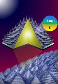
Above-11%-Efficiency Omnidirectional Hybrid Solar Cells
Hierarchical structures consisting of micropyramids and nanowires are used in Si/PEDOT:PSS hybrid solar cells to achieve a power conversion efficiency (PCE) up to 11.48% with excellent omnidirectionality, which is the highest PCE among all the reported Si/organic hybrid cells. The hierarchical-structured device properly designed by Dr. He’s team paves a promising way for developing low-cost, high-efficiency, and omnidirectional solar applications in the future.
Additional information can be found in the journal Nano Letters (J.H. He et al., “Above-11%-Efficiency Organic–Inorganic Hybrid Solar Cells with Omnidirectional Harvesting Characteristics by Employing Hierarchical Photon Trapping Structures,” Nano Lett. (Published online) (DOI: nl401540h))
|
 |
|
Figure 2. Hierarchical
hybrid solar cells |
|
|
Modeling of photoinitiated polymerization for active packaging of light-emitting diodes
Professor Ding-Wei Huang
Graduate Institute of Photonics and
Optoelectronics, National Taiwan University
We have presented a comprehensive modeling for the kinetics of photoinitiated polymerization. In our model, the light emitted from a bare LED chip was characterized by integrating the contributions of each infinitesimal area of the source. Next, the time evolution profile of the polymerization process trigger by LED intensity further can be solved by finite difference method. The percentage maps of the monomer concentration at different times describe the encapsulant profile by active packaging method for light-emitting diodes in thick polymer systems. With our simulation process, the shape and precise size of the mushroom-shaped lens can be depicted for any specific parameters in the polymerization reaction (e.g., LED power, polymerization time, absorptivity of the epoxy and photolysis, etc.) Lastly, our modeling provide useful guidance for designing the encapsulant shape by photoinitiated polymerization, such as the active packaging method, and it may inspire many applications such as encapsulation with multiple LED chips, or encapsulant lens design for special emission patterns. The study of the photoinitiated polymerization for fabricating self-written waveguides is under way in our laboratory.
|
 |
|
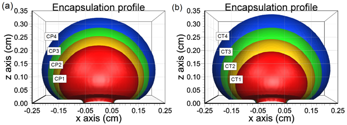
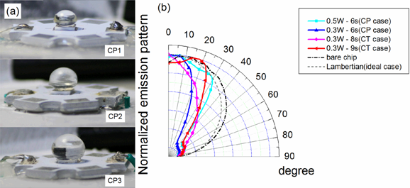
Figure 1. LED lens geometry simulated by the finite difference method. CP cases shown in (a). The simulation parameters are as follows. CP1: 0.3 W – 6 s, CP2: 0.4 W – 6 s, CP3: 0.5 W – 6 s, and CP4: 0.55 W – 6 s. CT cases shown in (b). The simulation parameters are as follows. CT1: 0.3 W – 6 s, CT2: 0.3 W – 7 s, CT3: 0.3 W –8 s, and CT4: 0.3 W – 9 s. |
|
 |
|
Figure 2. The geometry of LED lamps fabricated by the AP method. CP samples are shown in (a). The radiation patterns of CP and CT samples are shown in (b). |
|
Microwave Determination of Quantum-Well Capture and Escape Time in Light-Emitting Transistors
Professor Chao-Hsin Wu
Graduate Institute of Photonics and
Optoelectronics, National Taiwan University
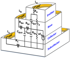
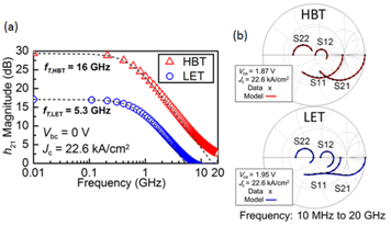
We demonstrated using microwave measurement (S-parameters) followed by small-signal analysis (Fig. 1) to determine the quantum-well (QW) capture and escape time of electrons in a light-emitting transistor (LET). The light-emitting transistor utilized embedded QWs in the base region of a heterojunction bipolar transistor (HBT) has been demonstrated with multi-GHz spontaneous optical bandwidth and recombination lifetime of a few ps.
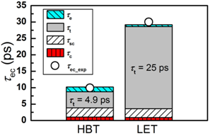
The emitter-to-collector transit time (τec) of the LET related to the transistor cut-off frequency (fT) (Fig. 2) is composed of emitter charging time (τe), base transit time (τt), space charge transit time in base-collector junction (τsc), and collector charging time (τc). We found that base transit time,
τt, of the LET is much longer than that of the conventional HBT (25 ps to 5 ps) under same bias condition (Jc = 22.6 kA/cm2) due to the experience of capturing/escaping processes caused by the embedded QWs in the base region of the LET (Fig. 3).
This work has been published in IEEE Trans. Electron Devices, vol. 60, 1088 (2013).
|
 |
|
Figure 1. HBT and LET device schematic layout (quarter) and the corresponding small-signal equivalent circuit model. DE = 13 μm, DB = 27 μm, and DC = 50 μm. |
|
 |
|
Figure 2. (a) Experimental h21 curves (red triangle: HBT; blue circle: LET). The extrapolation curves shows the cut-off frequency, fT, at 0 dB of the HBT is 16 GHz (corresponding τec=10 ps), and 5.3 GHz of the LET (corresponding τec=30 ps). (b) Measured and modeled S-parameters of the HBT and LET. The S-parameters were measured in common-collector configuration. |
|
 |
|
Figure 3. Stack column plot of the components of emitter-to-collector transit time of the HBT and LET. Open circles represent the experimental emitter-collector transit time obtained from cut-off frequency (Fig. 2.(a).). The HBT base transit time (τt = 4.9 ps) is close to theoretical calculation, and the LET base transit time (τt = 25 ps) includes carrier capture and escape time caused by QWs, which is about 20 ps. |
|
|