|
January 2013 - April 2013 |
| |
|
|
 |
|
 |
| |
Publisher:
Chairman Ching-Fuh Lin Editors:
Professor I-Chun Cheng, Ms. Hsiao-wen Lin May 30,
2013 |
| |
|
 |
|
Congratulations to the following GIPO students under the supervision of GIPO professor Jr-Hau He, on being awarded the Physical Society of Republic of China's 2012 Graduate Students'
Thesis Prizes:
|
Prize |
Winner |
Title |
Adviser |
|
Excellent |
Cheng-Han Ho
(Master student)
|
Efficient light harvesting/extraction schemes employing structure design from microscale to nanoscale for InGaN/GaN devices
|
Jr-Hau He |
|
Good |
Cheng-Ying Chen
(Ph.D. student)
|
Optoelectronic properties and electronic structures of one-dimensional semiconducting/piezoelectric nanostructures with sizes beyond the quantum confinement regime
|
Jr-Hau He |
Congratulations to GIPO Ph.D. student I-Wen Wu on being awarded, under the direction of GIPO professor Chih-I Wu, the 2012 Chien-Shiung Wu scholarship from the Physical Society of Republic of China.
|
Winner |
Title |
Adviser |
I-Wen Wu
(Ph.D. student)
|
Investigations of
interfacial properties in organic
light emitting diodes via impedance-voltage
characteristics |
Chih-I Wu |
Congratulations to Prof. Chi-Kuang Sun and Prof. Chung-Chih Wu on being awarded the “2012 Distinguished Research Award of National Science Council”.
|
|
 |
|
 |
|
| |
|
 |
|
December & January
“Photonics Forum” Highlights
(Compiled by Li-Chi Yao) |
|
|
Dec. 21st (Fri.), 2012,
3:30 pm |
|
Speaker: |
Dr. John Pern (National Renewable Energy Laboratory) |
|
Topic: |
An Introduction to CuInGaSe2 (CIGS) Thin-Film Solar Cell Technologies |
| |
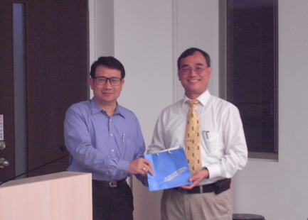
Dr. John Pern visited GIPO on Dec. 21st (Fri.) and delivered a speech titled “An Introduction to CuInGaSe2 (CIGS) Thin-Film Solar Cell Technologies” at room 205, Min-Da Hall. His speech was fabulous and action-packed, and Dr. Pern interacted well with the audience. The GIPO professors and students benefitted a great deal from the experience.
|
| |
|
 |
|
Dr. John Pern
(right) and GIPO chairman Ching-Fuh Lin, the host of this speech (left) |
|
|
|
Dec.
28th (Fri.), 2012,
3:30 pm |
|
Speaker: |
Prof. Devki N. Talwar (Chair of Department of Physics, Indiana U of Pennsylvania (IUP)) |
|
Topic: |
Nanotechnology: Making Efficient Solar Cells for Clean Energy |
| |
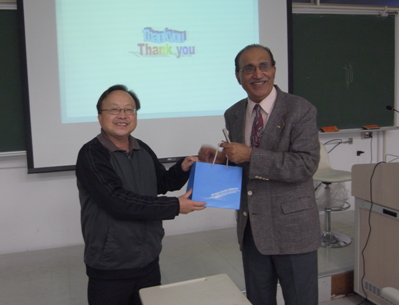
Prof. Devki N. Talwar visited GIPO on Dec. 28th (Fri.) and delivered a speech concerning “Nanotechnology: Making Efficient Solar Cells for Clean Energy” at room 205, Min-Da Hall. His speech was wonderful. The participants were eager to ask questions and benefitted greatly from the event.
|
| |
|
 |
|
Prof. Devki N. Talwar (right) and Prof. Zhe-Chuan Feng, the host of this speech (left) |
|
|
|
Jan. 4th (Fri.), 2013,
3:30 pm |
|
Speaker: |
Meng-Yin Ho (Manager, Photonics Industry & Technology Development Association) |
|
Topic: |
The Opportunities of Photonics Development & Its World Market |
| |
PIDA manager Meng-Yin Ho visited GIPO on Jan. 4th (Fri.) and delivered a speech titled “The Opportunities of Photonics Development & Its World Market” at auditorium 101, Barry Lam Hall. Her speech was filled with interesting information, including the themes : the variety of categories within the photonics industry, the present status of the global and Taiwan’s photonics industry, swiftly-emerging new display techniques, the soon-to-blossom LED lighting market, and movement of the production of the world’s PV to the Asia-pacific region. The GIPO professors and students participated in this event with great enthusiasm, interacted well with the speaker, and gained a lot from the experience.
|
| |
|
|
March
“Photonics Forum” Highlights
(Compiled by Li-Chi Yao) |
|
|
Mar. 1st (Fri.), 2013,
3:30 pm |
|
Speaker: |
Ms. Yu-Ting Chen (Member and the Honorary President of the Singapore Life Art Society) |
|
Topic: |
Untitled |
| |
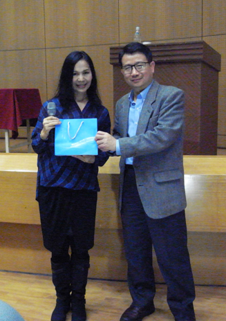
Ms. Yu-Ting Chen visited GIPO on Mar. 1st (Fri.) and delivered a speech at 101 auditorium, Barry Lam Hall. Her speech was untitled and she chiefly shared her experiences and the process of her striving and overcoming challenges in life. The speech was action-packed and interesting. The GIPO professors and students all took part in this event with enthusiasm and benefitted a great deal from it.
|
| |
|
 |
|
Ms. Yu-Ting
Chen (left) and GIPO chairman Ching-Fuh Lin, the host of this event (right) |
|
|
|
Mar. 8th (Fri.), 2013,
3:30 pm |
|
Speaker: |
Dr. Wanguo Liang (Fujian Institute of Research on the Structure of Matter, Chinese Academy of Sciences) |
|
Topic: |
The Research of the Industrialization of Crystal Materials to Laser Projectors |
| |
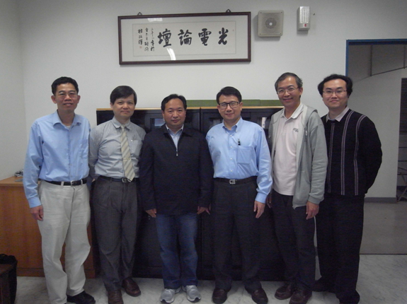
Dr. Wanguo Liang visited GIPO, at Prof. Lung-Han Peng’s invitation, on Mar. 8th (Fri.) and delivered a speech about “The Research of the Industrialization of Crystal Materials to Laser Projectors” at 101 auditorium, Barry Lam Hall. His speech was fascinating. The GIPO students attended the event, asked plenty of questions, and benefitted greatly.
|
| |
|
 |
|
A group photo of Dr. Wanguo Liang (left 3) and GIPO professors |
|
|
|
Mar. 22nd (Fri.), 2013,
3:30 pm |
|
Speaker: |
Prof. Russ Dupuis (Chaddick Endowed Chair in Electro-Optics, Georgia Institute of Technology, USA) |
|
Topic: |
MOCVD Quantum Well for LED and Lasers |
|
|
Mar. 22nd (Fri.), 2013,
4:30 pm |
|
Speaker: |
Prof. Shyh-Chiang Shen (School of Electrical and Computer Engineering, Georgia Institute of Technology, USA) |
|
Topic: |
III-Nitride Electronics for Next-Generation Energy Efficient Electronic Systems |
| |
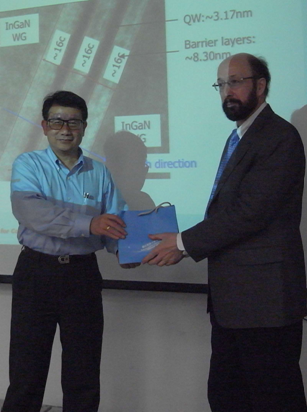
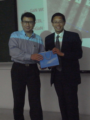
Prof. Russ Dupuis and Prof. Shyh-Chiang Shen visited GIPO on Mar. 22nd (Fri.) at Prof. Jian-Jang Huang’s invitation, and delivered speeches titled “MOCVD Quantum Well for LED and Lasers” and “III-Nitride Electronics for Next-Generation Energy Efficient Electronic Systems” at room 205, Min-Da Hall. Their speeches were wonderful and both professors interacted well with the audience. The GIPO professors and students had taken part in this event with enthusiasm and gained a lot from it.
|
| |
|
 |
 |
|
Prof. Russ
Dupuis (right, left photo),
Prof. Shyh-Chiang Shen (right,
right photo) and GIPO chairman Ching-Fuh Lin, the host of the speeches (left) |
|
|
|
Mar. 29th (Fri.), 2013,
3:30 pm |
|
Speaker: |
Prof. Pochi Yeh (Electrical and Computer Engineering, University of California, USA) |
|
Topic: |
3D Holographic Image Displays using Liquid Crystal Panels |
| |
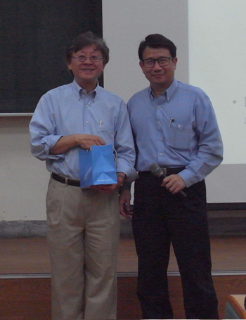
Invited by Prof. Sheng-Lung Huang, Prof. Pochi Yeh visited GIPO on Mar. 29th (Fri.). Professor Yeh spoke on the topic of “3D Holographic Image Displays using Liquid Crystal Panels” at 105 Lecture Theatre, EE II Building. His speech was fascinating, and the GIPO students who had enthusiastically attended this event gained a lot from it. |
| |
|
 |
|
Prof. Pochi
Yeh (left) and GIPO chairman Ching-Fuh Lin, the host of this speech (right) |
|
|
 |
|
 |
|
| |
|
 |
|
~
Optics & Photonics Taiwan, International Conference 2012 (OPTIC 2012)
~
(Time: Dec. 6th~8th, 2012; Location: Barry Lam Hall & Min-Da Hall, NTU)
OPT (Optics and Photonics Taiwan) is Taiwan’s most important event in optics and photonics for technology exchange each year. Every year, each university takes a turn to host this event, which has promoted Taiwan’s level of optics and photonics research by means of allowing exchanges of ideas among its related industries, authorities and academic scholars.
According to the resolution of the 1st joint meeting of OPT’s steering committee, held on May 8th, 2012 by Taiwan Photonics Society, starting from this year, the English name of OPT conference is changed to “Optics & Photonics Taiwan, International Conference”, abbreviated “OPTIC”. Nevertheless, its Chinese name “台灣光電科技研討會暨國科會光電學門研究成果發表會” remains the same.
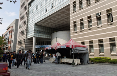
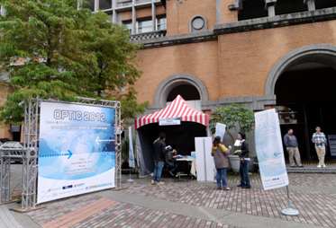
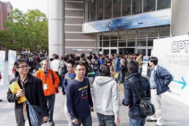
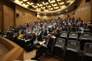
OPTIC 2012, held during Dec. 6th~8th, 2012 at Barry Lam Hall & Min-Da Hall, NTU, lasted 3 days. There were 1239 domestic and international scholars, students and industry specialists attending this conference. There were 9 major topics, including Nanophotonic Materials and Devices, Optical Waveguides and Communications, Quantum Optics and Laser Technology, Information Optics, Optical Design and Engineering, Biophotonics and Biomedical Imaging, Display Technology, Solid State Lighting Technology, and Photovoltaic Technology, and 822 technical papers presented, including 583 poster and 239 oral presentations.
Plenty of events occurred during this conference, including 8 plenary talks, 41 invited talks, panel discussion, contributed oral and poster presentations, student paper awards competition, and exhibition of 20 photonics manufacturers. The annual meetings of OSA Taiwan affiliate, IEEE Taipei affiliate, and Taiwan Photonics Society, and the National Science Council’s photonics research performance presentation were also held during this conference, which further promoted the exchanges among the students, scholars and specialists in photonics.
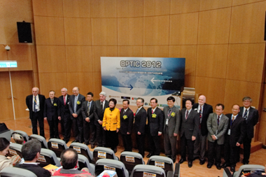
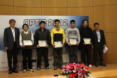
On the morning of Dec. 6th , the first day of the conference, we had especially invited Yung-Mau Chao, the administrative vice-president of NTU, Ching-Ji Wu, a national policy advisor to the president, Shu-Hung Shen, the minister of Environmental Protection Administration, and Hsiu-Lien Lu, ex-vice-president of R.O.C., to address the opening ceremony. Afterwards, there were 5 plenary talks, during which Dr. Woodrow W. Clark II, Prof. Satoshi Kawata, Prof. Lihong Wang, Dr. Burn Lin and Prof. Paul Weiss delivered speeches on green energy and the exploration of advanced photonics technologies. After the above wonderful speeches, Prof. Lihong Wang, Dr. Burn Lin, Prof. Paul Weiss, Prof. Michal Lipson, Prof. Eustace L. Dereniak and Dr. Kari Apter held panel discussions with the attendants. In the afternoon, the poster presentation sessions were held on the 3rd and 5th floors of Min-Da Hall, and the attendants exchanged the ideas on their research topics and learned from each other on the spot. On the morning of Dec. 7th, the second day of the conference, there were another 3 plenary talks. We had Prof. Xuechu Shen, Prof. Eustace L. Dereniak and Prof. Michal Lipson to deliver speeches about the exploration of advanced photonics technologies. Meanwhile, the poster sessions also continued on the 3rd and 5th floors of Min-Da Hall. In the afternoon, oral presentations and invited talks were held at Barry Lam Hall and Min-Da Hall. These talks attracted fervent discussion among the attendants. Then in the evening, there was a conference banquet. The domestic and international scholars, industry specialists, and professors and students from many universities all gathered together, which provided good opportunities for interactions. On Dec. 8th, the third day of the conference, the invited talks, oral presentations, and poster presentations continued. Finally, there was a closing ceremony, in which best student paper awards were given to 38 students.
In recent years, the development of photonics research is vigorously rising and flourishing in the domestic academic community. By holding this annual conference, we have not only provided opportunities for interaction, increased the research capacity in photonics related fields, but also expanded the cooperation between the academia and industry. Although everyone greatly valued this year’s conference, held in Barry Lam Hall and Min-Da Hall of NTU, we do fear that we have not done well enough, as the event came up against constraints in space and location. In the future, a larger conference location might go even further in increasing our international renown and improving our worldwide image.
This year’s conference has closed successfully and achieved its projected goals. We thank GIPO’s professors, students, conveners of all fields and everyone related for your strong support and kind participation to make this event perfect. The working staff has also gained precious experiences which will be extremely useful for future conferences.
|
 |
 |
|
The conference hall (Barry Lam Hall) |
The conference hall (Min-Da Hall) |
 |
 |
|
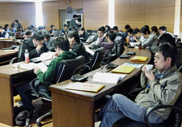
The attendants participated fervently |
A group photo of opening ceremony attendants |
 |
 |
|
A scene of enthusiastic participation in the auditorium |
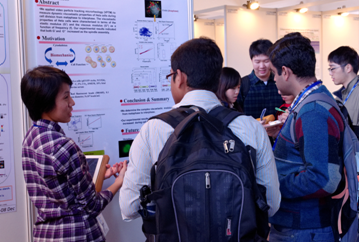
Lots of attendants gathered at the conference hall to listen to the discussion online |
 |
 |
|
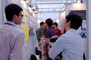
3rd floor of Min-Da Hall, the site of poster sessions |
5th floor of Min-Da Hall, the site of poster sessions |
 |
 |
|
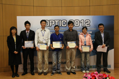
The ceremony of best student paper award |
The ceremony of best student paper award |
|
|
 |
|
 |
|
| |
|
 |
Passively mode-locked
erbium-doped fiber laser with graphite and charcoal
nano-particle
Professor
Gong-Ru Lin
Graduate Institute of Photonics and
Optoelectronics, National Taiwan University
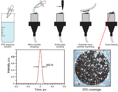
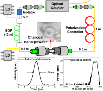
It is the first demonstration that the graphite nano-particle can
serve as a saturable absorber to passively mode-lock the erbium-doped fiber
laser (EDFL). By directly brushing the graphite nano-particle on the end-face of
a FC/APC with the assistance of polymer polyvinyl alcohol (PVA) film (see Fig.
1), such a novel approach greatly simplifies the fabrication procedure and
suppresses the film-thickness induced laser-beam divergent loss to promote the
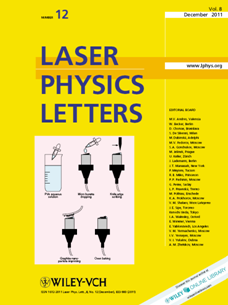
pulsewidth shortening ability. This work was select as the cover story of the
journal of Laser Physics Letters (see Fig. 2) and the highly cited paper. The
saturable absorber with an optimized area coverage ratio of 25% provides the
modulation depth of 20% to generate a passively mode-locked EDFL pulsewidth of
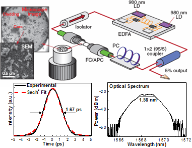
482 fs (Fig. 1). Later on, the free-standing graphite nano-particle is also
successful on mode-locking the EDFL without the assistance of PVA film; however,
the self-aggregated graphite nano-particles induce a high cavity loss to result
in a broadened pulsewidth of 1.67 ps and a time-bandwidth product of 0.325 under
an intra-cavity group delay dispersion of –0.017 ps2 (Fig. 3). The
graphite nano-particle with reduced size and sufficient coverage ratio can
effectively decrease the insertion loss and lasing threshold to compete with
other fast saturable absorbers such as carbon nanotube or graphene. In addition,
the triturated charcoal nano-powder is preliminarily used to passively mode-lock
the EDFL. These dispersant-free charcoal nano-powder with few crystalline
graphene phase and highly disordered carbon structure can easily provide a
passively mode-locked pulsewidth as short as 0.9-1.36 ps in a low-gain EDFL
(Fig. 4). The nanoscale charcoal saturable absorber shows its potential for
generating subpicosecond pulse under a relatively low cavity gain. An
appropriate cavity design can compensate the defect-induced loss to overcome the
limitation for obtaining a shortened pulsewidth in the near future.
 |
 |
|
Figure 1. Schematic diagram of the
direct brushing process and the
autocorrelation trace of the passively
mode-locked EDFL, as well as the image
of graphite nano-particle on the
end-face of FC/APC. |
Figure 2. The cover story of Laser
Physics Letters in vol. 8, pp. 880-886,
2011 (SCI Highly cited paper in 2012). |
 |
 |
|
Figure 3. The graphite nano-particle
based passively mode-locked EDFL system
with the autocorrelation trace and the
optical spectrum. |
Figure 4. The charcoal nano-particle
based passively mode-locked EDFL system
with the autocorrelation trace and the
optical spectrum. |
Applications of nanostructured materials for
organic/nano/hybrid optoelectornics
Professor
Chung-Chih Wu
Graduate Institute of Photonics and
Optoelectronics, National Taiwan University
We have been dedicated to development of nanostructured materials and their
applications to various organic/nano/hybrid optoelectronic devices, for
instance, nanostructured dye-sensitized solar cells (DSSCs). DSSCs offer various
advantages and are one of promising solar cell technologies. A typical DSSC
consists of transparent conductive substrate (anode), a porous thin-film
photoelectrode consisting of TiO2 nanoparticles, dye, electrolyte,
and a counter electrode. Each part of the cell has crucial effects on overall
cell efficiency. We had investigated the effects of nanostructured anodes
(transparent conducting oxides, TCO) on characteristics and performances of
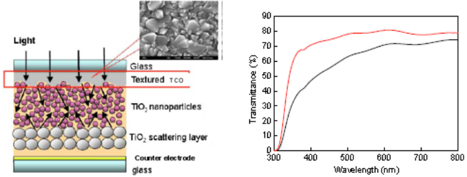
DSSCs. TCO having varied nano-textures were studied for their morpholoical,
electrical and optical properties and were subjected to device applications
(Fig. 1). Highly textured and high-haze TCO can effectively scatter the incident
light into larger angles in the device (Fig. 1), enhancing the propagation
length and trapping of the incident light within the device and enhancing
absorption/light harvesting (and thus short-circuit current, quantum efficiency,
and power conversion efficiency) of the device. We also investigated the
growth/formation of nano-textured/nanoporous /nanorod counter electrodes of
DSSCs (Fig. 2). Counter electrodes having varied nano-textured/nanoporous/nanorod
structures were characterized for their morphological and electrochemical
properties (Fig. 2), and were subjected to device applications. Highly nano-textured/nanoporous
/nanorod counter electrodes can effectively enhance active surface areas,
electrocatalytic ability and charge exchange at the interface with the DSSC
electrolyte (Fig. 2). By incorporating these effective nanostructured
electrodes, highly efficient DSSCs with reduced interface impedance were
achieved simply using typical dye sensitizers (Fig. 3).
 |
|
Fig. 1. (a) DSSC having nano-textured
TCO anode. (b) Normal-direction (red)
and integrated (black) transmittance
spectra of highly textured TCO anode,
showing high integrated transmittance
and strong optical scattering. |
 |
|
Fig. 2. (a) DSSC having nano-textured/nanoporous
/nanorod counter electrode. (b) SEM of
nano-textured/nanoporous /nanorod
counter electrode. (c) Cyclic
voltammetry (CV) and enhanced
electro-catalytic activity of nano-textured/nanoporous
/nanorod counter electrode. |
 |
|
Fig. 3. (a) I-V, (b) IPCE, and (c)
impedance spectroscopy and reduced
interface impedance of DSSC
incorporating nanotextured anode and
nano-textured/nanoporous /nanorod
counter electrode. |
The investigation of the diffusion length of cathode materials in organic light emitting devices through impedance characteristics
Professor
Chih-I Wu
Graduate Institute of Photonics and
Optoelectronics, National Taiwan University
The impedance-voltage (Z-V) characteristic is introduced as a non-destructive method to analyze the diffusion length of the cathode materials in organic light emitting diodes (OLEDs). The transition voltage is the voltage where the impedance decreases before the device turns on and the hole transport layer (HTL) becomes conductive. The electrical potential of each layer inside the OLED is illustrated in Fig 1, indicating that the transition voltage is determined by the density of the accumulation charges Q and the thickness of the electron transport layer (ETL). The phase-voltage, current density-voltage (J-V), and Z-V characteristics of devices with different thicknesses of the ETLs and various cathode structures are shown in Fig 2 and Fig 3, respectively. The correlations of the transition voltage and the thickness of the ETL of devices with varied film structures are also investigated systematically in Fig 4. The results reveal that the density of the accumulation charges at the organic layers interfaces is constant in devices with the identical carrier transport layers. However, the transition voltages shift toward higher bias voltages in the devices with a lower work-function metal as the cathode (Mg) or an electron injection layers (LiF or Cs2CO3). This shift of the transition voltages is attributed to the diffusion of the cathode atoms, which decreases the effective ETL thickness for providing the electrical potential between two electrodes, as shown in Fig 5. Based on this assumption, the diffusion length of the cathode materials being used can be estimated by the overall decreasing of the electrical potential, and the analysis of transition voltages in the Z-V is proposed as a potential method to measure the cathode atoms diffusion length in OLED devices.
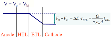 |
Fig 1. Illustration of the electrical potential inside the OLED devices at the transition voltage. The arrow indicates the difference between the turn-on voltage and the transition voltage. |
Efficiency improvement of organic solar cell through deposition rate control
Professor
Jiun-Haw Lee
Graduate Institute of Photonics and
Optoelectronics, National Taiwan University
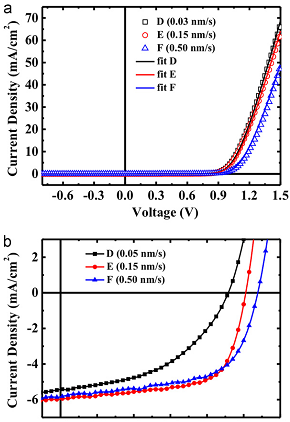
Increase of open circuit voltage (Voc) and fill factor (FF) were achieved in a small-molecules heterojunction solar cell by varying the deposition rate of donor material subphthalocyanine chloride (SubPc). With increasing the deposition rate of
SubPC, we found that: (1) energy level shifted away from the vacuum level, and (2) the molecular stacking tended to amorphous, which resulted from the increase of Voc. Besides, the mobility of subPC thin film decreased with increasing depostion rate, which affected the charge balance in such a device. With suitable treatment of anode layer, considerable improvement in both the VOC (1.02 V) and fill factor (65.37%) of the device, and a 3.96% final efficiency of the device was achieved. [published in Sol. Energy Mater. Sol. Cells.
103, 69, 2012].
|
 |
|
Fig. 1. The J–V characteristics of OPV devices at various SubPc deposition rates under (a) dark condition (hollow symbol: experiment results, line: fitting results) and (b) 1-sun AM 1.5G solar illumination. The deposition rates of SubPc in Device D, E, and F are 0.03 nm/s, 0.15 nm/s, and 0.50 nm/s, respectively. |
Effects of the spatial frequency composition of
the target pattern and the number of
quantization levels in diffractive beam shaper
design
Professor Hoang-Yan Lin
Graduate Institute of Photonics and
Optoelectronics, National Taiwan University
A mathematical model is derived and numerical
simulation is analyzed for laser beam shaping by using multi-level phase-only
diffractive optical elements. We used the simulated annealing algorithm to
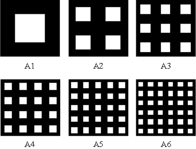
design the beam shapers. There is an essential effect on the diffractive pattern
quality caused by the spatial frequency composition of target patterns (Fig. 1)
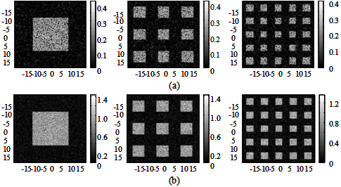
for the same incident Gaussian beam size and target pattern area. The root mean
square error between the diffractive and target patterns is smaller for the
target patterns with lower spatial frequencies (Fig. 2). Moreover, the effect of
spatial frequency composition can be relaxed for the cases of larger incident
Gaussian beam size (Fig. 3). Besides, finer quality controlling on diffraction
pattern can be obtained by increasing the number of quantization levels at the
diffractive optical elements.
|
 |
|
Fig. 1. Target patterns comprising of squares with various frequency compositions. |
|
 |
|
Fig. 2. The 4-level beam shapers designed for the target patterns (a) A1; (b) A3; and (c) A5, respectively by using R= 0.25 mm incident Gaussian beam. |
|
 |
|
Fig. 3. The diffractive patterns of the 4-level beam shapers by using (a) R= 0.25 mm; and (b) R= 0.50 mm incident Gaussian beams. |
Far-field self-focusing and -defocusing
radiation behaviors of the electroluminescent
light sources due to negative refraction
Professor JianJang Huang
Graduate Institute of Photonics and
Optoelectronics, National Taiwan University
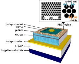
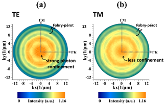
Negative refraction was observed from a semiconductor light source with embedded
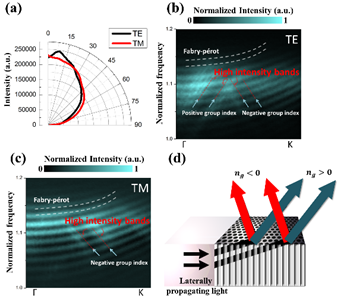
PhC nanohole arrays. For TE mode, when photons interact with the PhC, changes
between positive and negative group indices in the dispersive band structure
modulate the group velocity, resulting in the confinement of radiation light to
10°. On the other hand, TM-mode photons are less perturbed by the air hole
structure. This study uses 3D far-field analysis to visualize the energy
distribution radiating from the devices and EFC analysis to obtain the
group-velocity dispersion in PhCs. Theoretical and experimental results show
that the inward and outward propagating light collide intensely near the
Brillouin zone in the TE mode. The polarization-dependent spatial distribution
makes it possible to achieve self-collimated electroluminescent devices,
enabling negative refraction with short optical path lengths and larger
numerical apertures for devices such as lasers and LEDs.
|
 |
|
Fig. 1. Device structure of a photonic
crystal LED (PhCLED) with surrounding
nanohole arrays. |
|
 |
|
Fig. 2. (a) Electroluminescent radiation
profiles. (b) shows the measured TE
photonic band, and (c) shows the
measured TM. (d) Principle of the
negative refraction and light
collimation of PhC nanoholes under TE
light. |
|
 |
|
Fig. 3. Far-field radiation of the
PhCLED measured (a) for TE and (b) for
TM at a wavelength of 454 nm. |
|
|
|
 |
|
 |
|
| |
|
|
 |
|
 |
|
|
|