|
September 2012 - December 2012 |
| |
|
|
 |
|
 |
| |
Publisher:
Chairman Ching-Fuh Lin Editors:
Professor I-Chun Cheng, Ms. Hsiao-wen Lin February 28,
2013 |
| |
|
 |
|
Congratulations! Guan-Jhong Lin, a GIPO graduate student under the direction of Prof. Jr-Hau
He wins the "2012 Lam Research Award
(1st-class)".
Congratulations to GIPO Ph.D. student Hong-Jhang Syu on being awarded, under the direction of Prof. Ching-Fuh Lin, the student paper award of European Photovoltaic Solar Energy Conference and Exhibition (EUPVSEC).
By virtue of his thesis: "Silicon
Nanowire Array Morphology Dependant
Optical Characteristics and Influences
on Hybrid Solar Cells", GIPO student Hong-Jhang Syu
won the student paper award in EUPVSEC
2012. This prize was awarded to only one person in each session. Therefore, among 1843 presented papers, only 6 were awarded this rare honor; the chance of winning was 0.33%. (Please refer to the
related pictures
and
EUPVSEC
2012’s website for details.)
Congratulations! GIPO Professor Zhe-Chuan Feng receives the title of
"2013 SPIE Fellow".
Congratulations to GIPO Ph.D. student
Chih-Hsien Cheng on being awarded, under the direction of Prof. Gong-Ru Lin, the "Best Student Award of 2012 Asia Communications and Photonics Conference".
Congratulations to GIPO
Ph.D. student Li-Ko Yeh and postdoctoral researcher Kun-Yu Lai on being awarded, under the direction of Prof. Jr-Hau He, the "Excellent Poster
Award of 2012 Taiwan Association for Coatings and Thin Films Technology’s annual conference & National Science Council’s research project presentation".
Congratulations to GIPO graduate students Yuan-Fu Tsai and Guan-Jhong Lin on being awarded the "2012 Youth Thesis
Prize of The Chinese Institute of Electrical Engineering".
|
Place |
Name |
Adviser |
Thesis title |
|
1st |
Yuan-Fu Tsai |
Chi-Kuang Sun
|
Non-invasive Terahertz Blood Glucose
Measurement |
|
1st |
Guan-Jhong Lin |
Jr-Hau He
|
Photovoltaic Physics of InGaN/GaN
Multiple Quantum Wells |
Congratulations to GIPO graduate students Guan-Jhong Lin,
Chiung-Ting Wu and Yuan-Fu Tsai on being awarded the "21st
Student Thesis Prize of Taiwan Photonics Society".
|
Name |
Thesis title |
Adviser |
|
Guan-Jhong Lin |
Photovoltaic Physics of InGaN/GaN
Multiple Quantum Wells |
Jr-Hau He |
|
Chiung-Ting Wu |
Technique Development of
Fourier-domain Optical Coherence
Tomography |
C. C. (Chih-Chung) Yang |
|
Yuan-Fu Tsai |
Non-invasive Terahertz Blood Glucose
Measurement |
Chi-Kuang Sun |
Congratulations to GIPO Ph.D. student Yung-Hsiang Lin on being awarded, under the direction of Prof. Gong-Ru Lin, the "2012 Garmin scholarship".
The Optics &
Photonics Taiwan, International
Conference 2012 (OPTIC 2012) was hosted by GIPO and held during Dec. 6~8 at Barry Lam Hall and Ming-Da Hall of NTU. Congratulations to the participating GIPO students on being awarded numerous prizes.
|
Prizewinner |
Prize |
Adviser |
|
Yu-Feng Yin |
OPTIC 2012 Student Oral Paper Award
(Ph.D. student)
|
Jian-Jang Huang |
|
Shih-Che Hung |
OPTIC 2012 Student Oral Paper Award
(Ph.D. student)
|
Ching-Fuh Lin |
|
Yung-Hsiang Lin |
OPTIC 2012 Student Oral Paper Award
(Ph.D. student)
|
Gong-Ru Lin |
|
Hui-Hsin Hsiao |
OPTIC 2012 Student Oral Paper Award
(Ph.D. student)
|
Hung-Chun Chang |
|
Liang-Yu Su |
OPTIC 2012 Student Oral Paper Award
(Ph.D. student)
|
Jian-Jang Huang |
|
Shih-Ying Lin |
OPTIC 2012 Student Oral Paper Award
(Master student)
|
Gong-Ru Lin |
|
Yu-Hsiang Cheng |
OPTIC 2012 Student Oral Paper Award
(Master student)
|
Chi-Kuang Sun |
|
Shao-Hsuan Kao |
OPTIC 2012 Student Oral Paper Award
(Master student)
|
Ching-Fuh Lin |
|
Po-Kang Yang |
OPTIC 2012 Student Oral Paper Award
(Ph.D. student)
|
Jr-Hau He |
|
Wen-Yen Chang |
OPTIC 2012 Student Oral Paper Award
(Ph.D. student)
|
Yean-Woei Kiang |
|
Yu-Chieh Chi |
OPTIC 2012 Student Oral Paper Award
(Ph.D. student)
|
Gong-Ru Lin |
|
Wei-Fu Chang |
OPTIC 2012 Student Oral Paper Award
(Ph.D. student)
|
Jiun-Haw Lee |
|
I-Wen Wu |
OPTIC 2012 Student Oral Paper Award
(Ph.D. student)
|
Chih-I Wu |
|
Hong-Jhang Syu |
OPTIC 2012 Student Oral Paper Award
(Ph.D. student)
|
Ching-Fuh Lin |
|
Y. P. Lai |
OPTIC 2012 Student Oral Paper Award
(Master student)
|
Sheng-Lung Huang |
|
|
 |
|
 |
|
| |
|
|
|
September & October
“Photonics Forum” Highlights
(Compiled by Li-Chi Yao) |
|
|
Sep.
14th (Fri.), 2012,
3:30 pm |
|
Speaker: |
Prof. Yuhwa Lo (University of California San Diego, USA) |
|
Topic: |
Lab-on-a-Chip Device for Point-of-Care in-Vitro Diagnosis |
| |
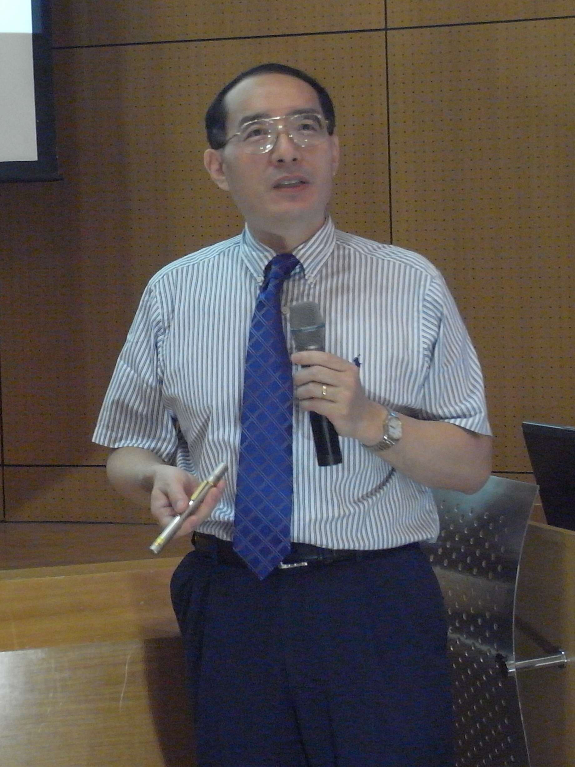
Prof. Yuhwa Lo visited GIPO on Sep. 14 (Fri.) and delivered a speech titled “Lab-on-a-chip device for point-of-care in-vitro diagnosis” at auditorium 101, Barry Lam Hall. The GIPO professors and students attended the event with enthusiasm and gained a lot from it. |
| |
|
 |
|
Prof. Yuhwa Lo (right) and GIPO chairman Ching-Fuh Lin, the host of this event (left) |
|
|
|
Oct. 5th (Fri.), 2012,
3:30 pm |
|
Speaker: |
Chung-Mo Cheng (Chairman, Taiwan Law & Policy Research Foundation) |
|
Topic: |
The Current Situation of Taiwan and the Way to Cope With It |
| |
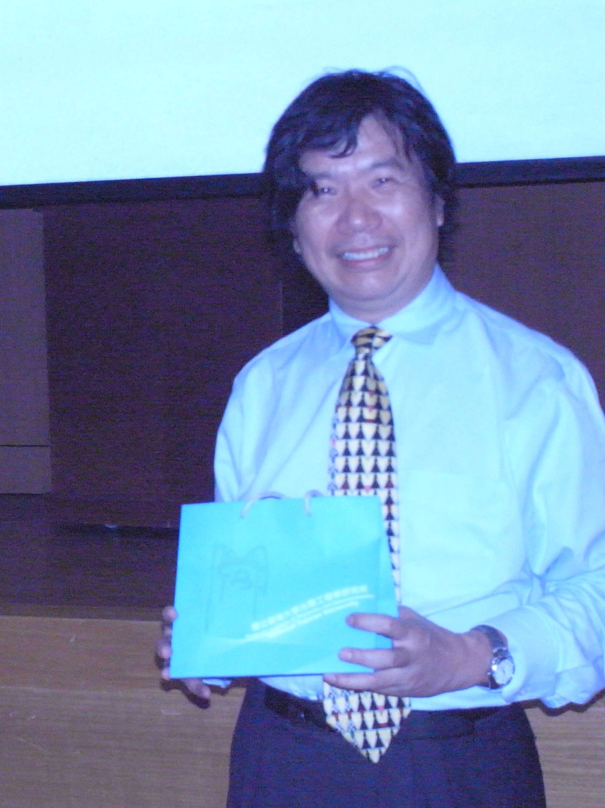
Chairman Chung-Mo Cheng visited GIPO on Oct. 5 (Fri.) and delivered a speech on “The Current Situation of Taiwan and the Way to Cope With It” at auditorium 101, Barry Lam Hall. GIPO students enthusiastically participated in this event and benefited greatly from it.
|
| |
|
 |
|
Chairman
Chung-Mo Cheng (right) and GIPO chairman Ching-Fuh Lin, the host of this event (left) |
|
|
|
Oct. 12th (Fri.), 2012,
3:30 pm |
|
Speaker: |
Prof. Yong-Hang Zhang (Electrical Engineering at Arizona State University) |
|
Topic: |
6.1 A II-VI and III-V Semiconductors and Their Applications for Optoelectronic and Electronic Devices |
| |
Prof. Yong-Hang Zhang visited GIPO on Oct. 12 (Fri.) and delivered a speech on “6.1 A II-VI and III-V semiconductors and their applications for optoelectronic and electronic devices” at auditorium 101, Barry Lam Hall. GIPO
professors and students took part in
this activity with great enthusiasm.
Prof. Yong-Hang Zhang’s speech was
filled with exciting content and the participants benefited greatly from the event.
|
| |
|
 |
|
The speaker, Prof. Yong-Hang Zhang |
|
|
|
Oct. 26th (Fri.), 2012,
3:30 pm |
|
Speaker: |
Prof. Sean TX Wu (Dept. of Information Management, Shih Hsin University; Interdisciplinary Program in Information Communications, NTU) |
|
Topic: |
Multi-learning, Independent and Inquisitive |
| |
Prof. Sean TX Wu visited GIPO on Oct. 26 (Fri.) and delivered a speech titled “Multi-learning, Independent and Inquisitive” at auditorium 101, Barry Lam Hall. GIPO professors and students attended the event with enthusiasm and gained a great deal from the experience.
|
| |
|
 |
|
The speaker, Prof. Sean TX Wu |
|
|
|
|
|
|
| |
|
|
|
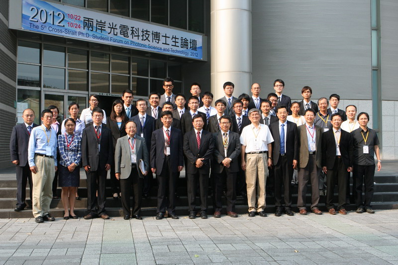
~ 2012 Ph.D. Student Academic Exchange with Nanjing University
~
(The 5th Cross-Strait Ph.D. Student Forum on Photonic Science and Technology, 2012)
(Time: October
20~26, 2012; Location: National Taiwan
University)
Composed by Chun-Wei Tsai, GIPO Ph.D.
candidate
The Ph.D. student exchange between GIPO of NTU and Physics
School of Nanjing University (NU) was hosted by GIPO and held at NTU this year. The Ph.D. student forum took place during Oct. 22~24. In addition to NU and NTU, we had also invited 24 Ph.D. students from Nanjing Normal University, Nanjing University of Technology, Soochow University and Nanjing University of Aeronautics and Astronautics to participate in this event. The scale of this year's exchange was greater than previous ones. It was the 5th time of the annual exchange between NU and NTU. I was honored to attend this event, and, by means of this experience, realized that both NU and NTU place more and more importance on the Ph.D. students’ interactions year by year.
In order to make this and the following exchanges proceed more smoothly,
Professor Ching-Fuh Lin, GIPO chair, and Professor Chih-I Wu, GIPO
vice chair, held 4 preparatory meetings and 1 review meeting. There were GIPO students
Yi-Jiun Chen, the team leader, Chia-Wei Liu, the
deputy leader, Jiun-Jie Chao, Dung-Sheng Tsai, I-Chung Chiu, Chun-Wei Tsai, Ling-Hsuan Tsai,
Yan-Shuo Chang, Liang Liao and Yung-Tsan Chen attending this interaction. Moreover, Hsiao-Wen Lin, GIPO clerk, handled the particulars of this year’s forum. Due to both professors' and students' all-out cooperation and detailed division of work, the event was carried out successfully. The event had 4 main themes: Ph.D. students' forum, cultural visits, laboratory visits and students' activities. I will hereunder report the details according to the agenda.
 |
|
A group photo of participants of
the 5th Cross-strait Ph.D. Student Forum on
Photonic Science and Technology. |
On the 1st day when the Mainland students arrived Taiwan, GIPO student leader
Yi-Jiun Chen and the team members went to pick them up at the airport. Then we dined at a restaurant across from the NTU campus gate. Almost all of our team members attended the dinner, and provided detailed explanation of the schedule to the NU and other Mainland universities' students. During the meal, we also talked about dietary habits, culture, history, university backgrounds and up-to-date news of both sides. After dinner, Ling-Hsuan Tsai and Yan-Shuo
Chang, the GIPO students taking care of our meals, thoughtfully gave our guests a tour of Gong-Guan night market. The Mainland students were deeply impressed by the Taiwan's night market culture and fine foods. But, because we had just eaten our fill at dinner, we could only say “no” to the temptation of those delicacies.
The next day was the cultural visit. Liang Liao was in charge of the excursion. He led us to
Yilan, the so-called backyard of Taipei. That day's visit was rich and colorful. In the morning, we went to Lan-Di
Stack Room to hear a narration of
Yilan's culture. In the afternoon, we went to
Hsing-Chien-Tsuen to hear an introduction of agroecology
and to experience making scallion pancakes and
rice noodles. In the evening, we went to Artemis
Garden to see, and smell, the fragrance of
aromatic plants. And, finally, we went to Jiaoxi, the famous hot spring scenic spot, to have diner and experience "hot spring fish SPA". Among these activities, the experiences of handmade scallion pancake and rice noodle at Hsing-Chien-Tsuen
and the "hot spring fish SPA" at Jiaoxi impressed us most. On the morning of the third day, we went to visit the famous National Palace Museum. Seeing the incredible collection of National Palace Museum had greatly impressed the Mainland students, who lingered without any thought of leaving.
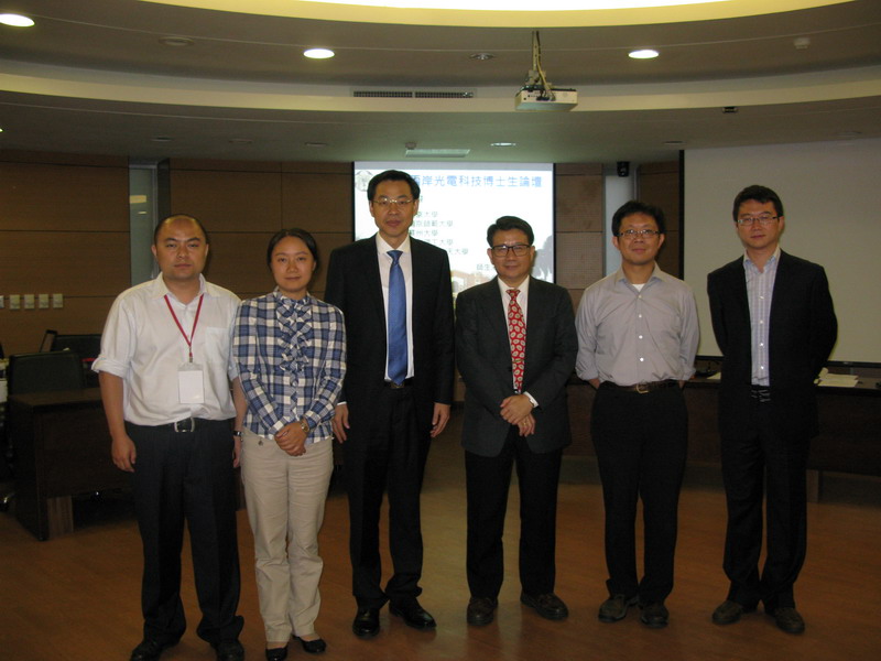 |
|
A
group photo at the forum site, from left to
right: Xiang Xiong (teacher, NU), Yan Ju (teacher, NU),
Zhenlin Wang (vice dean, NU), Ching-Fuh Lin (GIPO chairman, NTU), Chih-I Wu (vice chairman, NTU), Peng-Fei
Qiu (teacher, NU) |
The major event of this interaction
- The 5th Cross-Strait Ph.D. Student Forum on Photonic Science and Technology - took place in the afternoon of the third day. Professor Ching-Hua Lo, Vice President for Academic Affairs, NTU,
Professor Ching-Fuh Lin, GIPO chair, NTU,
Professor Shining Zhu, Physics School, NU/member of the Chinese Academy of Sciences, and
Professor Zhenlin Wang, vice dean,
Physics School, NU, co-hosted the
3-day-long Cross-strait Ph.D. Student
Forum on Photonic Science and
Technology. From the forum, we realized
that they, students of NU and the other
Mainland universities, had focused their
study on analyses of fundamental science
and theories, which was quite different
from our focus of applied engineering
and hands-on experience. We deeply
admired them for their knowledge of
fundamental science and theories.
Because of this difference, both sides
discussed studies frequently during and
after the forum. Although we admired
their fundamental science and theory
studies, they were also very interested
in our applied engineering studies. Many
of them admired us more for our
immediate application of our studies.
During the 3-day forum, students from
both sides all did their best to explain
their studies so as to let others
understand their research filed, focuses
and results through the detailed
reports. Generally speaking, both sides'
students did well in briefing and
questioning; everyone had good stage
presence. In particular, NU and other
Mainland universities' students raised
numerous questions with enthusiasm; this
put us under some pressure, and is
certainly an area that we should improve
on. The key program of this year's
interaction was for one side's students
to choose the other side student's best
thesis and best interaction-with-others.
In the end, Yanfei Bai, Physics School, NU, and
Chun-Wei Tsai, GIPO, NTU, won the best thesis prizes; Li Wang, Physics
School, NU, and Yi-Jiun Chen, GIPO, NTU,
won the best relationship-with-others
prizes. Of course, we would also like to
thank Jiun-Jie Chao, Dung-Sheng Tsai, Yung-Tsan Chen and
Chun-Wei Tsai for their help in setting the agenda and arranging the meeting locations. Because of their generous assistance, all activities of the forum proceeded as planned.
 |
|
A group photo of all attending Ph.D. students of NTU, NU, Nanjing Normal University, Nanjing University of Technology, Soochow University, and Nanjing University of Aeronautics and Astronaut, at the forum site. |
On the afternoon of the fifth day, after the forum was over, we had laboratory visits. I-Chung Chiu arranged for our guests to visit GIPO laboratories, including: Prof. Ching-Fuh Lin's "Silicon
Photonics and Organic Solar Cell Lab.", Prof. Chih-I Wu's "OLED
Meterial Analysis Lab.", Prof. I-Chun Cheng's "Flexible
Optoelectronics Laboratory", and Prof. Jr-Hau He's "Small
Lab.". After the visit, the Mainland students all admired GIPO's professors and students very much for we could achieve the best research results in the most limited laboratory spaces. In other words, the arrangement and usage of our laboratories maximized benefits. On the sixth day, we went to Hsinchu Science Park to visit EPISTAR and AU Optronics Corporation. Through visiting these two large companies, the Mainland students could have further understanding of the up-to-date development of Taiwan's photonic industry.
On the morning of the last day, we arranged free time for our guests so they could go anywhere they wished to visit or try any Taiwanese local delicacy. In the afternoon, GIPO chair, Prof. Ching-Fuh Lin, and the rest of us went to Leader Hotel to see each of them off. During the farewell, the Mainland professors and students were deeply touched by NTU professors and students' hospitality and sadness at seeing them go. And thus, this cross-strait Ph.D. student exchange came to a perfect end.
|
|
|
|
|
|
| |
|
|
|
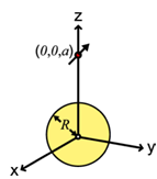
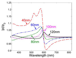
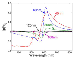
Theoretical Study of Surface Plasmon Coupling between a Radiating Dipole and a Metal Nanoparticle
Professor Y. W. Kiang’s Laboratory
Graduate Institute of Photonics and
Optoelectronics, National Taiwan University
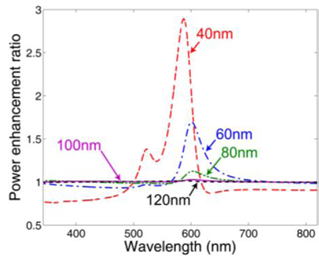
We report the theoretical and numerical study results of surface plasmon (SP)-dipole coupling based on a simple coupling model between a radiating dipole and the SP induced on a nearby Ag nanoparticle (NP). To include the dipole strength variation effect caused by the field distribution built in the coupling system (the feedback effect), the radiating dipole is represented by a saturable two-level system. The spectral and dipole-NP distance dependencies of dipole strength variation and total radiated power enhancement of the coupling system are demonstrated and interpreted. The results show that the dipole-SP coupling can enhance the total radiated power. The enhancement is particularly effective when the feedback effect is included and hence the dipole strength is increased. Figure 1 shows the geometry of the dipole-NP system, including a spherical Ag NP with radius R (=10 nm) centered at the coordinate origin and a radiating dipole located at (0, 0, a), which is represented by an arrow. Figure 2 (3) shows the dipole strength enhancement ratios,  , of the x-oriented (z-oriented) dipole as functions of wavelength when the distance between the dipole and the Ag NP center, a, varies from 40 through 120 nm. Figure 4 (5) shows the total radiated power enhancement ratios as functions of wavelength at several a values for the x-oriented (z-oriented) dipole. The power ratio is defined as the total radiated power of the dipole-NP system over that in the case without the Ag NP. , of the x-oriented (z-oriented) dipole as functions of wavelength when the distance between the dipole and the Ag NP center, a, varies from 40 through 120 nm. Figure 4 (5) shows the total radiated power enhancement ratios as functions of wavelength at several a values for the x-oriented (z-oriented) dipole. The power ratio is defined as the total radiated power of the dipole-NP system over that in the case without the Ag NP.
 |
 |
 |
|
Figure 1 |
Figure 2 |
Figure 3 |
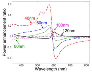 |
 |
|
Figure 4 |
Figure 5 |
|
Structural properties of InAsPSb grown on GaAs
Professor Hao-Hsiung Lin
Graduate Institute of Photonics and
Optoelectronics, National Taiwan University
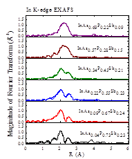
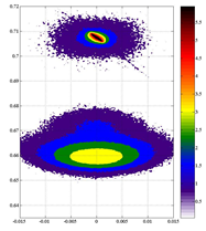
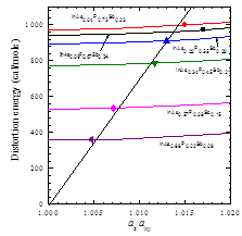
Previous studies have shown that bonds in alloy resemble their original lengths in binaries. Quaternary InAsPSb contains two bonds, InP and InSb, that are with very large mismatch in length. This mismatch leads to strong bond distortion in the quaternary, which could affect the structural, electronic and optical properties. In this work, we investigate the structural properties of InAsPSb grown on GaAs substrate using reciprocal space mapping (RSM) and P K-edge and In K-edge extended X-ray absorption fine structure (EXAFS). Valence force field (VFF) is used to simulate the bond distortion in the quaternary. Fig. 1 shows the Fourier transformed In K-edge EXAFS signals. Two peaks representing InP and InSb bonds are clearly seen when As composition is low and gradually merge into a broad peak with the increasing As composition. Detailed analysis show that the bond lengths are close to their original values in binaries. Fig. 2 shows RSM results of a InAsPSb samples. Although the lattice mismatch between of these alloys and GaAs is ~7% and the layer thicknesses are 1000 times thicker than the critical thicknesses, strong residual strain exists in these layers. We used VFF model to calculate the bond distortion. Fig. 3 shows the distortion energy as a function of az/axy for each sample. As can be seen, the distortion energy is much larger than the strain energy and the residual strain, in term of az/axy ratio, is proportional to the distortion energy. This finding suggests that the randomly oriented bond distortion could hinder the generation of dislocation in the alloy, leading to the observed residual strain.
 |
 |
 |
|
Fig. 1 Fourier transformed In K-edge
EXAFS signal of InAsPSb. |
Fig. 2 (004) and (-1-15) RSM
measurements of InAs0.04P0.73Sb0.23
show a az/axy ratio of 1.017, resulting
from the residual strain in the 1-mm-thick
sample. |
|
|
|
 |
|
Fig. 3 Distortion energy as functions of
az/axy for InAsPSb
alloys. Symbols indicate the az/axy
ratio obtained from RSM measurement for
each samples. |
Crystalline Si Thin Foil of Completely Single Domain
Professor Ching-Fuh Lin
Graduate Institute of Photonics and
Optoelectronics, National Taiwan University
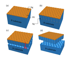
Producing ultra-thin Si wafer with low Si material waste is an important issue to achieve grid parity of Si solar cells. Although Si wafer with a thickness of 20μm can be fabricated by epitaxial techniques, these techniques need rigorous process environment, expensive equipment and high power consumption, limiting the potential of cost reduction. In this report, we explore a procedure involving very fast and low-cost process to fabricate crystalline Si thin foils of completely single domain from (100) Si bulk wafer.
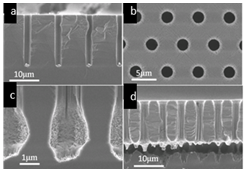
The low-cost procedure is a multi-step metal-assisted etching (MAEtch). Figure 1 shows the procedure of forming Si thin foil using multi-step MAEtch. First of all, the Ag used as catalytic agent for MAEtch is deposited on the Si surface with photoresist (PR) pattern. The solution of electroless metal deposition consists of AgNO3 and HF, which allows Ag+ to become silver dendrites on Si. Second, the multi-step MAEtch has two major steps including anisotropic and isotropic etching. The solution of the anisotropic etching (1st step MAEtch) is composed of H2O2 and HF to form vertically-aligned Si micro-holes. In aqueous solution of H2O2 and HF, Ag dendrites will sink into Si substrate vertically. Then, at the other MAEtch step (2nd step MAEtch), the Si micro-holes from the 1st step MAEtch are undercut for lift-off of Si thin-foil. The solution of 2nd step MAEtch contains a large H2O2/HF ratio to achieve isotropic etching, and thus Si micro-holes could be undercut from the bottom. Figures 2(a) and (b) are the SEM images of the micro-holes formed in 1st step MAEtch, where vertical micro-holes can be observed. In Fig. 2(c) and (d), the micro-hole undercut with isotropic etching is also shown, and the thin foil can be lifted-off after 7-min of 2nd step MAEtch. By multi-step metal-assisted etching, the entire procedure takes no more than 20 minutes to produce the Si thin foil with thickness of 15 μm.
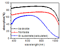
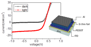
The Si thin foil with micro-hole structure could induce strong light trapping effect, leading to high absorption. Figure 3 shows that the absorption of the Si thin foil is over 85% from 350 nm to 960 nm, exceeding the calculated absorption of planar Si thin foil with the same thickness. This is due to the fact that the back side of the thin foil provides excellent anti-reflection, and multiple internal light scattering is induced by the micro-hole structure. Finally, combined with solution-processed conducting polymer, the Si thin foil/PEDOT:PSS solar cell is demonstrated. The structure of the solar cell is depicted in inset of Fig.4. The interface between the PEDOT layer and n-type Si can form a good heterojunction for separation of electron-hole pairs, and it reveals rectifying characteristics as shown in Fig.4. In conclusion, the Si thin foil has potential for low-cost solar cell devices, and its light-weight and ultra-thin properties can enable wide applications.
 |
 |
 |
|
Figure 1. (a) Deposition of silver on the PR -patterned Si surface. (b) 1st step MAEtch to form vertically-aligned Si micro-holes. (c) 2nd step MAEtch to undercut the Si micro-holes. (d) Lift-off of the Si thin foil from Si substrate.
|
|
Figure 2. (a) & (b) are side-view and top view of the Si micro-holes formed by 1st step MAEtch, respectively. (c) Side view of Si micro-holes after 2nd step MAEtch for 2min. (d) Side view of Si micro-holes after 2nd step MAEtch for 5min.
|
 |
|
 |
|
Figure 3. Absorption spectra of the Si thin foil.
|
|
Figure 4. J-V characteristics of Si thin foil/PEDOT solar cell under dark and light conditions. Inset picture: Device structure of the Si thin foil/PEDOT solar cell.
|
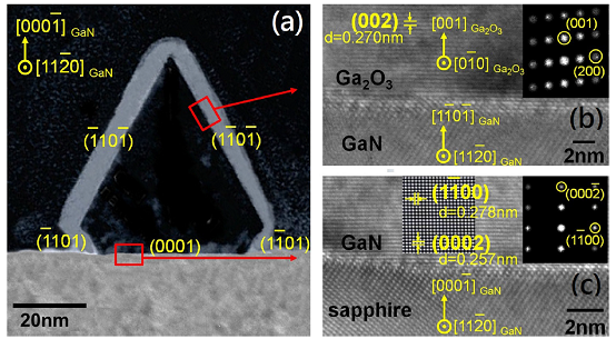
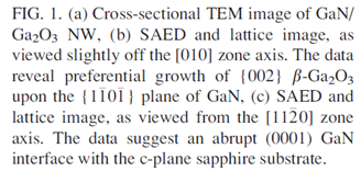
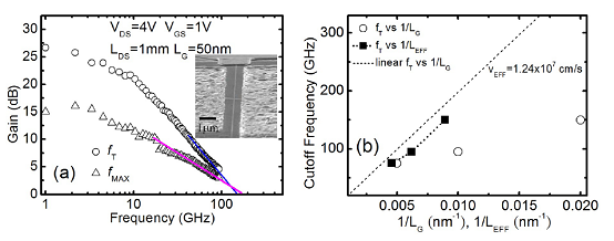
Short channel effects on gallium nitride/gallium oxide nanowire transistors
Professor
Lung-Han Peng
Graduate Institute of Photonics and
Optoelectronics, National Taiwan University
To explore the carrier transport properties in the short channel regime, we used the technique of electron-beam lithography to define transistors with drain-source distance LDS of 1μm, and gate length of Lg= 500, 200, 100, and 50nm on the same wafer where the [ ]-GaN/Ga2O3 NWs were grown. GaN/Ga2O3 nanowire metal-oxide-semiconductor field-effect-transistors (NW-MOSFETs) are shown to operate at average electron velocity of ~1.24×107cm/sec and threshold-voltage roll-off of -0.2V as the transistor gate length Lg reduced from 500 to 50nm. Improvement of saturation current to 120μA and unity current/power-gain cut-off frequency to 150/180GHz are observed on Lg=50nm devices. This concurs with doubling of the device peak transconductance gm value from 42μS of the long-gate value to 84μS of the short gate devices. Moreover, a drain induced barrier lowering (DIBL) factor (measured at a drain current of 10 mA/mm for VDS =1 and 4V) below 35mV/V was observed in the GaN/Ga2O3 NW-MOSFETs compared with a DIBL value of ~50mV/V commonly observed in the planar-type devices. Our study reveals the advantages of using (i) polarization-induced positive charge and high-k dielectric at { ]-GaN/Ga2O3 NWs were grown. GaN/Ga2O3 nanowire metal-oxide-semiconductor field-effect-transistors (NW-MOSFETs) are shown to operate at average electron velocity of ~1.24×107cm/sec and threshold-voltage roll-off of -0.2V as the transistor gate length Lg reduced from 500 to 50nm. Improvement of saturation current to 120μA and unity current/power-gain cut-off frequency to 150/180GHz are observed on Lg=50nm devices. This concurs with doubling of the device peak transconductance gm value from 42μS of the long-gate value to 84μS of the short gate devices. Moreover, a drain induced barrier lowering (DIBL) factor (measured at a drain current of 10 mA/mm for VDS =1 and 4V) below 35mV/V was observed in the GaN/Ga2O3 NW-MOSFETs compared with a DIBL value of ~50mV/V commonly observed in the planar-type devices. Our study reveals the advantages of using (i) polarization-induced positive charge and high-k dielectric at { }GaN/{002}Ga2O3 to provide carrier confinement and to shield the drain field, and (ii) polarization-induced negative charge at (0001)GaN/sapphire to form back-barrier to suppress leakage and improve the short-channel transport properties. }GaN/{002}Ga2O3 to provide carrier confinement and to shield the drain field, and (ii) polarization-induced negative charge at (0001)GaN/sapphire to form back-barrier to suppress leakage and improve the short-channel transport properties.
Ref: C.-W. Yu et al., “Short Channel Effects on Gallium Nitride/Gallium Oxide
Nanowire Transistors,” Appl. Phys. Lett. 101, 183501 (2012).
Cell death detection by quantitative three-dimensional single-cell tomography
Professor
Sheng-Lung Huang's
Laboratory
Graduate Institute of Photonics and
Optoelectronics, National Taiwan University
The aim of cancer therapies is mainly to stop cell proliferation or induce cell death. Cell death regulation is important for normal development and homeostasis. Cancer cells escape from death signals and continue their abnormal proliferation. Therefore, the ability to induce death in cancer cells has been a crucial biomarker for the efficacy of chemotherapeutic agents. However, individual cancer cells, even from the same population, vary greatly in their response to cell death stimuli. Measuring the response at the single-cell levels provide further pharmacokinetic and pharmacodynamics information, which aids drug development and regimen design. Developing a microscopic technology with non-invasive,
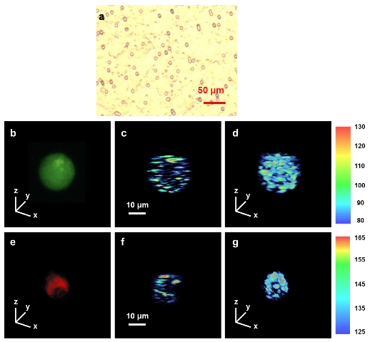
in situ, label-free, single-cell spatial resolution may serve this long-term need. We report the detection of cell death at the single-cell level using ultrahigh-resolution optical coherence tomography (UR-OCT). An improvement in OCT technology currently provides axial resolution to approximately 1 μm and lateral resolution to 2 μm. We demonstrated that UR-OCT not only provides three-dimensional
in situ single-cell imaging but is also able to delineate subcellular structure (i.e., the nucleus). Dead cells cannot be differentiated from live cells based merely on size. Many parametric analytic methods have been used to address this issue, including speckle fluctuation in time-lapse images. It was confirmed that back-scattering signals are lower in apoptotic cells, which is most likely due to the perturbation of mitochondria morphology during apoptosis. Nuclear disintegration after chromatin condensation provides high-signal-intensity peaks that facilitate the identification of apoptotic cells.
With the collaboration between GIPO team at National Taiwan University (NTU) and Professor Jeng-Wei Tjiu’s team at the NTU
Hospital, a homemade UR-OCT system was developed to image single-cell basal cell
carcinoma (BCC) in three dimensions and differentiate between live and dead BCC
cells by not only morphological recognition but also parametric analysis. The
BCC cell line was used because BCC is the most common skin cancer, and we are
familiar with it. An image analysis approach was also developed to automatically
extract deterministic information of a single cell.
This result is featured at http://www.octnews.org in October 2012.
 |
|
Fig. 1. Microscopic image of BCC cell
line and UR-OCT/confocal microscopy
images of live and dead BCC cells. BCC
cell line was suspended in Matrigel and
imaged by a bright-field microscope (a).
Live and dead BCC cells were randomly
selected from the sample and scanned by
UR-OCT and confocal microscopy. Live
cell were encoded in green (b) and dead
cell which was were encoded in red (e),
according to the calcein and propidium’s
fluorescence spectrum. Two-dimensional
cross-sectional imaging (c, f) were
performed across the center of each
cell. Three-dimensional imaging of the
whole cell (d, g) were realized by
combining several cross-sectional images
whose covering range were slightly
larger than the size of the cells. |
Semiconductor Nanorod-based Nanoacoustic and Nanoultrasonic Technologies
Professor
Chi-Kuang Sun’s Laboratory
Graduate Institute of Photonics and
Optoelectronics, National Taiwan University
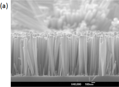
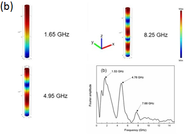
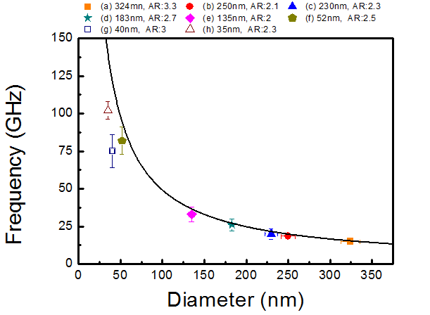
Led by NTU GIPO, laser-based nanoultrasonic technology is one of the most innovative tools for the noninvasive sub-surface nano-imaging. For the present nano-fabrication processes (22/32/45nm), it provides a possible solution to nondestructively monitor the yielding rate for mass production. Thanks to the piezoelectric multilayer structures and the ultrafast optical coherent control, we successfully photo-generated and synthesized the acoustic waveform with <10 nm wavelength, which determined the longitudinal resolution of a nanoultrasonic image. However, the lateral resolution is still severely restricted by the optical diffraction limit. Besides the previously demonstrated saturation technology, one way to improve the lateral resolution is to use nanorods as nanoultrasonic sources and probes. In order to realize the application, our laboratory currently has devoted to the comprehensive investigation of nanoacoustic vibrations in nanorods, including multiple orders of extensional and radial breathing modes. Figure 1 shows the SEM picture of the GaN nanorod array. We successfully measured several quantized (confined) vibrational modes in the studied nanorods, of which the frequencies agree well with the predicted results by using a finite element method (FEM) simulation. Figure 2 shows the oscillation frequency of the fundamental radial breathing mode as a function of rod diameter. We discovered that the mechanical properties, e.g. elastic stiffness constant C11, in piezoelectric GaN nanorods start to differ from those of bulk GaN when the rod diameter shrink down to the order of or less than 50nm. That is, the softening effect in nanorods was observed once the rod diameter was reduced to <50 nm. In brief, we have well characterized the various confined vibrational modes of nanorods. The explored information serves as a foundation for future nanorod-integrated nanoultrasonic technologies.
  |
|
Figure 1 (a) SEM picture of nanorods array. The average length is 1150 nm and the average diameter is 100 nm. (b) Observed acoustic spectrum and FEM simulation of the mode shapes of the extensional modes. |
 |
|
Figure 2 Measured oscillatory frequency as a function of rod diameter. The horizontal error bars represent the diameter nonuniformity based on the SEM images and the vertical error bars represents FWHM of the amplitude in Fourier-transformed oscillatory spectra. The black curve shows the theoretical oscillation frequencies of the radial breathing modes. |
|
|
|
|
|
|
|
| |
|
|
 |
|
 |
|
|
|