|
|
 |
|
 |
| |
Publisher:
Chairman Ching-Fuh Lin Editors:
Professor I-Chun Cheng, Ms. Hsiao-wen Lin October 30,
2012 |
| |
|
 |
|
May
“Photonics Forum” Highlights
(Compiled by Li-Chi Yao) |
|
|
May 11th (Fri.), 2012,
3:30 pm |
|
Speaker: |
Chun-Ting Liu (Deputy
Director, Electronics and
Optoelectronics Research
Laboratories, Industrial Technology
Research Institute) |
|
Topic: |
Advanced LED
and OLED Lighting Technologies |
| |
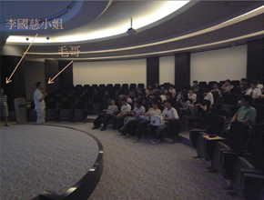
Deputy Director Chun-Ting Liu
visited GIPO on May 11th
(Fri.) and delivered a speech
“Advanced LED and OLED Lighting
Technologies” at auditorium 101,
Barry Lam Hall. His speech was
splendid and well-considered in
every respect. He interacted
thoughtfully with the GIPO
professors and students. Everyone
participated with great enthusiasm
and thus benefited greatly from the
talk.
|
| |
|
|
June
“Photonics Forum” Highlights
(Compiled by Li-Chi Yao) |
|
|
June 1st (Fri.), 2012,
3:30 pm |
|
Speaker: |
Prof. Yeong-Chuan Kao
(Department of Physics,
National Taiwan University) |
|
Topic: |
How Did Einstein Form
the Principle of Special Relativity
and the Concept of Light Quantum? |
| |
Professor Yeong-Chuan Kao visited
GIPO on June 1st (Fri.)
and delivered a speech “How Did
Einstein Form the Principle of
Special Relativity and the Concept
of Light Quantum?”. The outline of
Professor Kao’s speech was to
elaborate on Einstein’s way of
thinking, and, especially, his
motive and logic of demonstration
when he delivered, in 1905, 2
important works concerning light:
the principle of special relativity,
and the hypothesis of quantum of
light. Professor Kao’s speech was
well-considered in every respect and
he interacted with the audience
throughout the speech. GIPO
professors and students attended the
event enthusiastically and thus
benefited greatly from it.
|
| |
|
 |
|
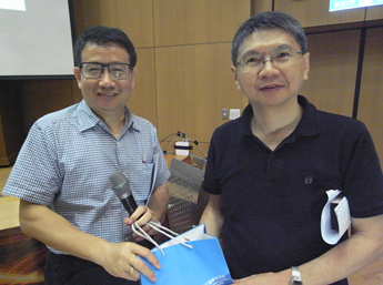
A group photo of
Professor Yeong-Chuan Kao
(right) and Chairman Ching-Fuh
Lin (left), the host of this
speech |
|
|
|
June 8th (Fri.), 2012,
3:30 pm |
|
Speaker: |
Prof. Asif Khan
(University of South Carolina,
Columbia SC, USA) |
|
Topic: |
Deep Ultraviolet
Light Emitting Diode Lamps |
| |
Professor Asif Khan visited GIPO on
June 8th (Fri.) and
delivered a speech on “Deep
Ultraviolet Light Emitting Diode
Lamps” at auditorium 101, Barry Lam
Hall. His speech was marvelous, and
the GIPO students participated in
this event with enthusiasm. The
participants were eager to ask
questions and benefitted greatly
from the experience.
|
| |
|
 |
|
The speaker,
Professor Asif Khan |
|
|
|
June 15th (Fri.), 2012,
3:30 pm |
|
Speaker: |
Dr. Cheng-Tsung Guo
(Institute of Nuclear Energy
Research, Atomic Energy Council, R.O.C.) |
|
Topic: |
High Concentration
Photovoltaic (HCPV) Technology |
| |
Dr. Cheng-Tsung Guo visited GIPO on
June 15th (Fri.) and
delivered a speech concerning “High
Concentration Photovoltaic (HCPV)
Technology” at auditorium 101, Barry
Lam Hall. The GIPO professors and
students participated in this event
with enthusiasm. Dr. Guo’s speech
was excellent, and he interacted
well with students. Everyone
benefited greatly from this event.
|
| |
|
 |
|
The speaker,
Dr. Cheng-Tsung Guo |
|
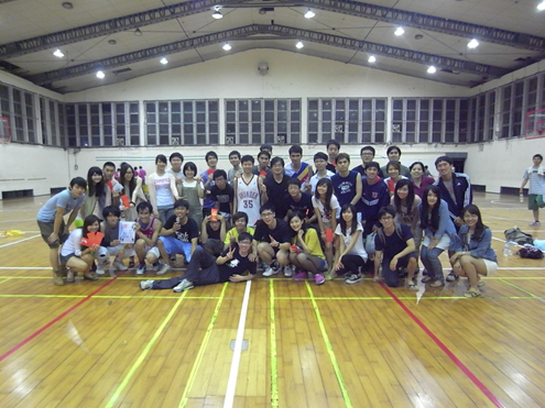
~
Highlights of the GIPO Students’
Association’s Optoelectronics Cup
Tournament ~
(Time: May 19th, 2012;
Location: Gymnasium, subdivision of
National Taiwan Normal University
Campus)
Compiled by Chi-Fan Huang,
President of GIPO Students’
Association
After several delays caused by Taipei’s
bad weather, the annual Optoelectronics
Cup Tournament was finally held on May
19th at the gymnasium of
subdivision of National Taiwan Normal
University Campus. This was the first
time GIPO opened the tournament to 2
types of ball games, badminton and
basketball, at the same time. Because of
the considerable prize and the
on-the-spot lottery, there was a great
deal of excitement among students and
everyone registered for the game with
enthusiasm. There were 6 teams
registered for badminton tournament and
22 teams for basketball’s 3-on-3. After
the opening ceremony, hosted by Chairman
Ching-Fuh Lin at 6 pm, the intense and
exciting basketball game started. In
order to ensure the impartiality, we
invited the head referee of the High
School Basketball League to perform the
job. After 2 hours’ fiery competition,
the team of professor Ding-Wei Huang’s
laboratory, the team of professor Gong-Ru
Lin’s laboratory and the team of
professor Chao-Hsin Wu’s laboratory had
made it to the final. In the final, the
competition was fierce. Having defeated
the other 2 teams, the team of professor
Ding-Wei Huang’s laboratory finally won
the championship, and the team of
professor Gong-Ru Lin’s laboratory
placed 2nd. It’s also worth
mentioning that some members of those 3
final teams were also co-workers of our
association for this event, which means
GIPO students are excellent both in
study and sports.
Following the 3-on-3 games, we had the
3-pointer jumper game. There was 45
students registered for this game, which
was a record-breaking in the history of
GIPO tournament. Finally, Shu-Wei Yeh, a
student from professor Sheng-Lung
Huang’s laboratory, emerged as the
champion.
This year’s badminton game was the first
ever held in the GIPO history. We were
surprised to see so many teams (6 in
total) registered, since, in a group
game, several members are needed to form
a team. Obviously, a great number of
people in GIPO are passionate about
badminton. We were also pleased to see
many women taking part in this event.
This was precisely why we added
badminton to the tournament, to
alleviate the problem of having mostly
male and few female participants. At the
end, the team of professor Chih-I Wu’s
laboratory won this championship and the
team of Ming-Hua Mao’s laboratory placed
2nd.
After a day-long competition, we
believed GIPO students got to know each
other better, and get closer. In fact,
all members of professor Jian-Jang
Huang’s laboratory came to the
tournament to cheer their friends on.
For those who participated in this
event, the activities will certainly be
a happy memory in his/her dreary life as
a graduate student.
Self-introduction of the President of GIPO Students’ Association of the 2012
Academic Year
 Hi,
GIPO professors, office staff and
students! I’m pleased to be the
President of the GIPO Students’
Association of the 2012 academic year
and to be able to have the opportunity
to serve you. My name is Yi-Jiun Chen
(陳奕均), which is only one word different
from the name of our GIPO professor
I-Chun Cheng (陳奕君). However, Professor
I-Chun Cheng is a Ph.D. of Princeton
University and I’m just a Ph.D.
candidate who can’t eat too much food
that is high in purine. I’m studying in
Professor Hoang-Yan Lin’s display optics
laboratory. Next semester will be the 2nd
year in my Ph.D. study. My office is
located at 351A, EEⅡ Building. You are
more than welcome to drop in for a chat
when you have either study problems or
questions about GIPO. Hi,
GIPO professors, office staff and
students! I’m pleased to be the
President of the GIPO Students’
Association of the 2012 academic year
and to be able to have the opportunity
to serve you. My name is Yi-Jiun Chen
(陳奕均), which is only one word different
from the name of our GIPO professor
I-Chun Cheng (陳奕君). However, Professor
I-Chun Cheng is a Ph.D. of Princeton
University and I’m just a Ph.D.
candidate who can’t eat too much food
that is high in purine. I’m studying in
Professor Hoang-Yan Lin’s display optics
laboratory. Next semester will be the 2nd
year in my Ph.D. study. My office is
located at 351A, EEⅡ Building. You are
more than welcome to drop in for a chat
when you have either study problems or
questions about GIPO.
Last year, when I took part in an
education appraisal, an appraiser said
to me: “It seems that NTU students
seldom care about things beyond
themselves, especially the graduate
students. They are always buried
themselves in their own studies.” At
that time, I was actually a shy person,
a man of few words and unable to get
along with others. However, because of
his words, I started actively took part
in the GIPO Students’ Association’s
business, and actively interacted with
my classmates. I was involved in the
GIPO Optoelectronics Camp, Sports
Tournaments, and the welcoming party
events for the new students. I also
participated in last year’s academic
exchange between GIPO and Nanjing
University. Being the President of the
students’ association, I would like to
promote the interaction among GIPO
students, hoping you can take part in
activities beyond study. I also
sincerely wish that after graduation you
will remember not only classmates of
your own laboratory but also classmates
of other laboratories, and you will keep
in touch with them and continue to
establish good relationship with
everyone.
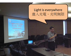
In conclusion, I’d like to quote
Chairman Ching-Fuh Lin’s slogan “light
is everywhere”, and, in this academic
year, I will be at your service
everywhere.
~
Highlights of the GIPO 2012
Undergraduates’ Optoelectronics Summer
Camp ~
(Time:
July 17~19, 2012;
Location:
Barry Lam Hall, NTU)
Compiled by Yi-Jiun Chen,
President of GIPO Students’ Association
This was the second time I took part in
holding the GIPO Undergraduates’
Optoelectronics Summer Camp. At the
first time, I led students to visit
laboratories. This time I, as the new
president of GIPO students’ association,
accompanied students for the whole -threeday
activities. I was so excited on the
previous night that I couldn’t fall
asleep, and I was late for the check-in
on the next day…
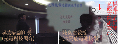
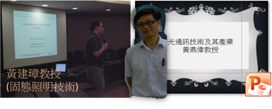
Professor Chih-I Wu, vice chairman of
GIPO, started the camp on the 1st
day by briefing students on
optoelectronics technologies, including:
organic and inorganic LED lighting,
display panels, solar cells and optical
communications. He also briefly analyzed
the future trend of the industry;
however, he didn’t elaborate much and
left students to find out the details in
the following lessons. Next, Professor
I-Chun Cheng elaborated more deeply
about solar cells, and, in the
intervals, she led students to the top
floor of Barry Lam Hall to see the solar
cell modules and explained how to
perform experiments using this
apparatus. After a brief break,
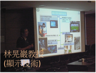
Professor Hoang-Yan Lin spoke to
students about display panels, including
the hot 3D display techniques. After
lunch, Professor Hoang-Yan Lin, who in
charge of undergraduate’s
optoelectronics experiments, again gave
students related lessons in order to
prepare for the introductory
optoelectronics laboratory. At that
time, I went to the optoelectronics
laboratory, in EEⅠ Building, to prepare
for the experiment setup. Then, working
together with two teaching assistants,
we introduced the experiments to
students.
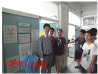
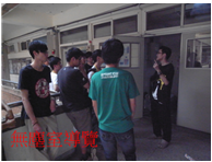
The laboratory tours included visiting
some of EEⅡ laboratories and a brief
introduction of the clean room. The
hands-on experiment in the EEⅠ
optoelectronics laboratory was also
included. During the event, I had the
opportunity to chat with the students
and realized that they came from various
departments, such as electronics
engineering, information engineering,
chemical engineering, oceanographic
engineering and optoelectronics-related
departments. Even though they have
different backgrounds, they were all
interested in and looking forward to
join the optoelectronics industry.
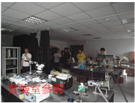
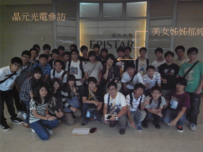
The next day, we went to Hsinchu Science
Park to learn about the optoelectronics
industry. We would like to thank Epistar
Corporation and AU Optronics Corporation
for making this visit possible. We went
to Epistar first and were received by a
beautiful lady – Yu-Ting Wang, manager.
Aside from introducing the assembly
line, she also clearly described
Epistar’s internal conditions and its
employee’s relationships. From her
introduction of the office of employee
relationships in Epistar, we could sense
Epistar’s kindness in taking care of its
employees in every possible way. The
beautiful lady said engagement was the
best policy in handling employee’s
relationships. During lunch, we talked
with Epistar’s superintendents
enthusiastically and believed that
everyone had learned something from this
visit. Next, we went to Au Optronics
Corporation and were received by Ms.
Guo-Tz Lee, who accompanied us even
though she was pregnant. Then AU’s
brother Mao (who asked us to call him by
this) gave us a lesson and wanted us to
think about how to revive the world’s
display panel industry. After the
lesson, he took us to visit the sports
facilities in the AU employee’s leisure
center. After that, in the products
display room, Ming-Hsien Lee, vice
manager, Advanced Manufacturing Section,
AC Technology department, introduced to
us all sizes of display panels. This
concluded the on-day visit and we drove
back to National Taiwan University.
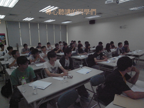
In the 1st class on the last
day of the camp, Professor Jian-Jang
Huang introduced the solid-state
lighting technology. After having
visited Epistar Corporation on the
previous day, students could understand
better on the solid-state lighting
lesson. In the last two classes,
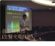
Professor Ding-Wei Huang spoke about
optical communication technology and
Professor Chia-Wei Sun discussed
biomedical optoelectronics, which then
concluded all the lessons of the camp.
After having a light meal, Chairman
Ching-Fuh Lin came to talk face-to-face
with the students, and the students were
eager to ask questions. Finally, the
chairman conferred the certificates
personally to each student and shook
hands and took photos with them. We
believe that all students have learned a
great deal from participating in this
camp.
Finally, we would like to thank Ms.
Li-Chi Yao of the GIPO office and
students Sheng-Hao Chen, Chai-Yu Shen,
Er-Hsuan Wu, Yan-Shuo Chang and Pei-Yu
Tseng for their help in making this camp
a great success.
|
 |
|
 |
|
| |
|
|
|
Study of Optical Anisotropy in Nonpolar and Semipolar AlGaN Quantum Well Deep Ultraviolet Light Emission Diodes
Professor Yuh-Renn Wu's
Laboratory
Graduate Institute of Photonics and
Optoelectronics, National Taiwan
University
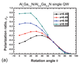
This study analyzes the optical
polarization characteristics and
internal quantum efficiency of AlGaN
based polar, nonpolar, and semipolar
deep ultra-violet(UV) LED. A 1D model is
used to solve drift-diffusion, Poisson
equations and 6x6 k.p Schodinger
equations to investigate band structure
and emission characteristics. The light
emission polarization ratios of nonpolar
and semipolar AlGaN based deep UV LED
with different Al compositions and
injection current were studied. The
studies shows that the optical
polarization of c-plane AlGaN based deep
UV LED is dominated by the out-plane
polarization as the Al composition
increases. And for the nonpolar
structures, the light polarization
direction is mainly dominated by
in-plane polarized light which is good
for surface emitting. Although the
anisotropic polarization property of
semipolar structures is not as strong as
the nonpolar structure, it can be
another choice if the growth speed is
faster than the nonpolar plane. Finally,
the study discusses IQE behavior through
changing the p-type activation energy,
quantum well layer number, and Schottky
barrier height. The detail work can be
found in our recent publications.
  |
|
FIG. 1. (a) The polarization
ratio rz’ of
a single AlGaN based deep UV QW
with different
rotation angle θ.
(b) The polarization ratio ρx′y′ of
a single AlGaN based deep UV QW
with
different rotation angle θ. |
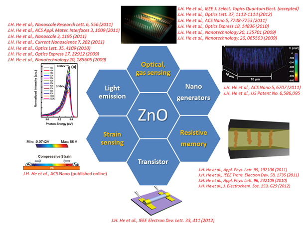
Surface Effect and Device Application of Nanostructured ZnO
Professor Jr-Hau He
Graduate Institute of Photonics and
Optoelectronics, National Taiwan
University
Nanostructured ZnO has attracted
intensive research efforts for its
versatile applications such as
nanogenerators, stain sensors,
field-effect transistors, light emitting
diodes, gas sensors, optical sensors,
and resistive memory. The surface
effects including surface band bending,
chemisorption/photodesorption near
surfaces, native surface defects/states,
and surface roughness are more
pronounced in the nanostructures than
that in thin film and bulk counterparts
due to the structural uniqueness and the
ultrahigh surface-to-volume ratio of ZnO
nanostructures. For the past years, we
have continued to understand how the
physical properties are affected by
shrinking the dimension of ZnO for
exceeding state-of-the-art planar
devices and developed the novel
application of ZnO nanostructures
utilizing the surface effect.
For more details, please visit our web
(http://cc.ee.ntu.edu.tw/~jhhe).
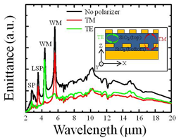
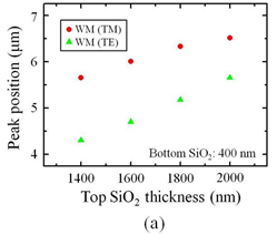
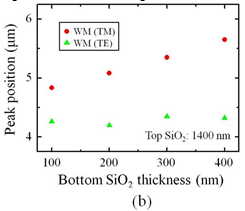
Two infrared emission modes with different wavelengths and orthogonal polarization in a waveguide thermal emitter
Professor Si-Chen Lee
Graduate Institute of Photonics and
Optoelectronics, National Taiwan
University
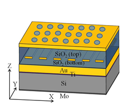
We investigated an Au/SiO2/Au
waveguide thermal emitter
incorporating a metallic grating
embedded in the SiO2 layer
(Fig. 1). The metal grating acts as
a beam splitter, dividing the device
into two waveguide structures
determined by the polarization of
the waveguide modes. The thermal
radiation spectrum exhibits two
peaks with orthogonal polarization
(Fig. 2). The emitted wavelengths of
the two waveguide modes can be
adjusted by controlling the
thickness of the SiO2 layers
on both sides of the metallic
grating (Fig. 3(a) and 3(b)). The
emission peaks have ratios of the
full width at half maximum to the
peak wavelength of 0.057 and 0.05
for the TE and TM polarizations,
respectively. These characteristics
show the suitability of the device
for multipeak and narrow bandwidth
infrared light source applications.
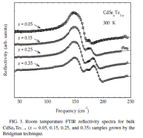
Combined Experimental and Theoretical Studies on II-VI Ternary CdSeTe and CdZnTe Alloys
Professor Zhe-Chuan Feng
Graduate Institute of Photonics
and Optoelectronics, National
Taiwan University
The optical, structural, and
electrical properties of
luminescent II-VI compound
semiconductors with bandgap
energies ranging from 0 to 4 eV
are appealing for ultrasensitive
multiplexing/multicolor
applications in a variety of
emerging areas of biotechnology,
nanoscale optoelectronics, and
nanophotonics. By varying the
composition and controlling the
lattice constants in ternary or
quaternary alloys, we can
achieve greater flexibility of
tuning emission and absorption
wavelengths for high-efficiency
solid-state light emission
sources. Earlier, the
applications of II-VI materials
for photonic devices were
hampered primarily by the
availability of poor-quality
crystals and the difficulty of
managing doping. Progress in the
modern crystal growth techniques
such as metalorganic chemical
vapor deposition (MOCVD),
molecular beam epitaxy (MBE)
etc., has offered higher quality
and greater versatility in the
preparation of thin films with
controlled doping on many
convenient substrates.
CdSexTe1-x is
the II-VI-VI ternary compound,
possesses a zinc-blende
structure for x<0.36. The
ability to prepare zinc–cadmium
(mercury)–based binary [AB,
with lended A =
Zn, Cd, and Mn (Hg) and B =
S, Se, and Te] compounds and
thin films of ternary A1−xBxC (e.g.,
Cd1−xZnxTe,
CdTe1−xSex,
etc.) or quaternary A1−x−yBxCyD (e.g.,
Cd1−x−yZnxMnyTe,
CdSexSyTe1−x−y ,
etc. where C and D can
be the elements of the binary
compound AB)
alloys with precise chemical
compositions x, y has
now opened up many possibilities
of using II-VI materials in
various technological
applications.
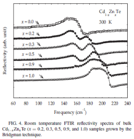
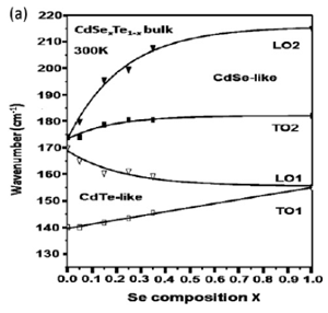
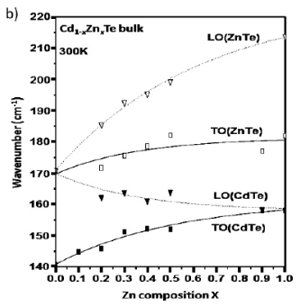
We have measured far-infrared (FIR) reflectance spectra for CdSeTe and CdZnTe alloys, as shown above, and in collaboration with Prof. Devki Talwar, an excellent theorist, also theoretical calculations on their phonon dispersions, as shown below [1]. Further, to II-VI compound semiconductors, we have used a comprehensive Green’s function theory to study the vibrational properties of isotopic defects and to ascertain the microstructure of complex centers involving dopants and intrinsic impurities. [2]
[1] Devki N Talwar, Tzuen-Rong Yang, Zhe Chuan Feng and P. Becla, “Infrared reflectance and transmission spectra in II-VI alloys and superlattices”, Physical Review B 84, 174203 (2011).
[2] Devki N. Talwar, Zhe Chuan Feng and Tzuen-Rong Yang, “Vibrational signatures of isotopic impurities and complexes in II-VI compound semiconductors”, Physical Review B 85, 195203 (2012).
Determination of Surface Plasmon
Modes and Guided Modes Supported
by Periodic Subwavelength Slits
on Metals Using a
Finite-Difference
Frequency-Domain Method Based
Eigenvalue Algorithm
Professor Hung-chun
Chang
Graduate Institute of Photonics and
Optoelectronics, National Taiwan
University
An eigenvalue solution algorithm is
formulated based on the
finite-difference frequency-domain (FDFD)
method for determining guided modes,
including the surface plasmon modes,
supported by periodic metallic
structures. The Yee-mesh grids which
have been popularly adopted in the
finite-difference time-domain (FDTD)
method are used in the FDFD method
and standard eigenvalue matrix
equations are obtained for easily
searching for the guided eigenmodes.
Both two-dimensional (2-D) and
three-dimensional (3-D) structures
are considered and the periodicity
is along the propagation direction.
The metals are assumed to be perfect
ones or real ones without loss. For
2-D structures, an array of grooves
drilled in a perfect conductor and a
real-metal structure with a periodic
arrangement of subwavelength slits
in air are analyzed and the
dispersion diagrams and mode-field
profiles are obtained. For the
latter structure, surface plasmon
modes and dielectric slab modes are
identified to be in agreement with
published results based on a
different numerical scheme. This
subwavelength-slit structure is then
extended to a 3-D one having an
additional depth and it is
demonstrated that the formulated
algorithm can solve the same two
kinds of modes for the more
complicated 3-D problem. The modes
guided along drilled periodic
rectangle holes on a perfect
conductor surface are also
calculated. (IEEE/OSA
Journal of Lightwave Technology,
vol. 30, no. 1, pp. 76–83, 1 January
2012.)
  |
|
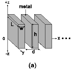
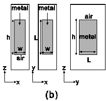
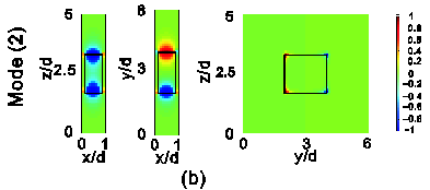
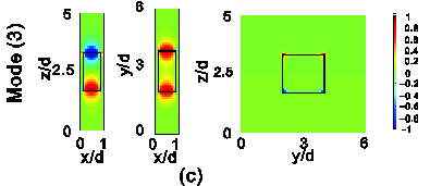
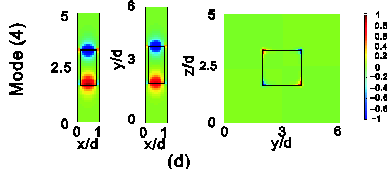
Fig. 1. (a) Schematic of the
3-D structure generalized
from the 2-D periodic
arrangement of subwavelength
slits. (b) Schematic of the
three sides of one metallic
block in the x-z, x-y,
and y-z planes. |
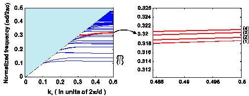 |
|
Fig. 2. Dispersion diagram
of the guided modes on the
structure of Fig. 1. The red
solid lines represent
surface plasmon modes and
the blue solid lines
represent a series of
effective dielectric slab
modes. The right panel is
the expanded view for more
clear visualization of the
surface plasmon modes. |
|
 |
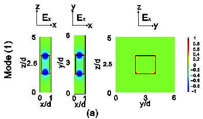
|
Fig. 3. Ex field
profiles at kx = p/d on
the three sides of one
metallic block, as plotted
in Fig. 1(b), i.e., in the x-z, x-y,
and y-z planes,
for each of the four suface
plasmon modes mode in Fig.
2. (a) Mode (1). (b) Mode
(2). (c) Mode (3). (d) Mode
(4). |
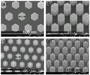
Regularly Patterned InGaN/GaN
Quantum-well Nanorod
Light-emitting Diode Arrays
Professor C.
C. (Chih-Chung) Yang's group
Graduate Institute of Photonics
and Optoelectronics, National
Taiwan University
With the nano-imprint
lithography and the pulsed
growth mode of metalorganic
chemical vapor deposition, a
regularly-patterned, c-axis
nitride nanorod (NR) array of
quite uniform geometry with
simultaneous depositions of
top-face, c-plane
disc-like and sidewall, m-plane
core-shell InGaN/GaN quantum
well (QW) structures is formed.
The differences of geometry and
composition between these two
groups of QW are studied with
scanning electron microscopy,
cathodoluminescence, and
transmission electron microscopy
(TEM). In particular, the strain
state analysis results in TEM
observations provide us with the
information about the QW width
and composition. It is found
that the QW widths are narrower
and the indium contents are
higher in the sidewall m-plane
QWs, when compared with the
top-face c-plane
QWs. Also, in the sidewall m-plane
QWs, the QW width (indium
content) decreases (increases)
with the height on the sidewall.
The observed results can be
interpreted with the migration
behaviors of the constituent
atoms along the NR sidewall from
the bottom.
 |
 |
|
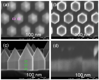
Fig. 1 Plan-view (a) and 30o-tilted (b) SEM images of the GaN NR array; Plan-view (c) and 30o-tilted (d) SEM images of the QW NR array. |
Fig. 2 Plan-view SEM (a) and the co-located panchromatic CL (b) images of the QW NR array; Cross-sectional SEM (c) and the co-located panchromatic CL (d) images of the QW NR array. The rectangles in (a) and (c) indicate the locations of local CL spectrum measurements. |
 |
 |
|
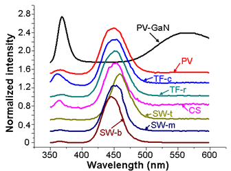
Fig. 3 CL spectra of the QW NR array measured at different locations and different view directions, including that from the large-scale plan-view (PV) measurement, that at the center on the top face of an NR (TF-c) and that at the rim on the top face of the NR (TF-r), that from the large-scale cross-sectional view (CS) measurement, that at a point near the top of the sidewall (SW-t), near the middle height of the sidewall of the NR (SW-m), and near the bottom of the sidewall of the NR (SW-b). The plan-view CL spectrum of the bare GaN NR array is also plotted as curve PV-GaN. |
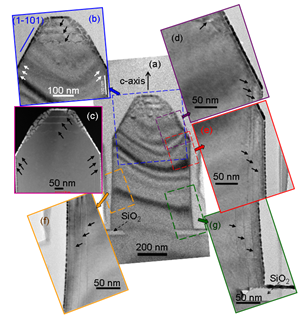
Fig. 4 (a) Cross-sectional TEM image of a QW NR. The portions of the top, the slant (1-101) facet on the right, the top sidewall on the right, the middle-height sidewall on the left, and the bottom sidewall on the right of the NR are magnified to show parts (b) and (d)-(g), respectively. The HAADF image of the NR top portion is shown in part (c). |
|
|
|
|
|
|
|
| |
|
|
 |
|
 |
|
|
|