|
High-order
Rational Harmonic Mode-locking and
Pulse-amplitude Equalization of SOAFL
under Optical Injection
Professor Gong-Ru Lin
Graduate Institute of Photonics and
Optoelectronics, National Taiwan
University
First
of all, we demonstrate the 20th-order
rational harmonic mode-locking (RHML)
semiconductor optical amplifier fiber
laser (SOAFL) pulses by using 1 GHz
backward dark-optical comb injection,
and discuss the
competition between
mode-locking mechanisms in the SOAFL at
high-gain and strong optical injection
condition at higher RHML orders.
As the rational harmonic order increases
up to 20, the auto-correlation traces
and optical spectra of the RHML-SOAFL at
different RHML orders are characterized.
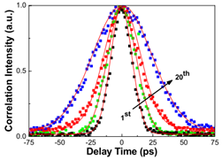
The Fig. 1. shows that the normalized
auto-correlation traces of the SOAFL at
1st, 5th, 10th,
and 20th RHML orders
gradually changes the pulsewidth from
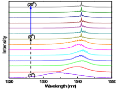
13.5 to 35 ps. The Fig. 2.
exhibits that the SOAFL spectrum with
red-shifted wavelength and reduced
linewidth from 12 to 3 nm at RHML order
increases to >8 reveal a less pronounced
high-order RHML mechanism when competing
with the continuous-wave lasing
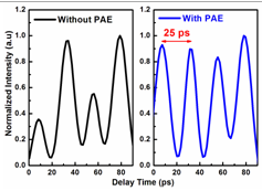
mechanism. Furthermore, in order to
solve the problem of uneven RHML
pulse-amplitude, we use the reshaped
10-GHz gain-switching FPLD double-peak
pulse to reconstruct the gain profile of
SOA in time domain, the 4th-order
RHML-SOAFL is demonstrated for achieving
40-GHz RHML pulse-train with optimized
performance of pulse-amplitude
equalization (PAE). The Fig. 3. shows
the auto-correlation traces of 4th-order
RHML pulse-train without and with PAE.
Such the indirect gain compensation
further balances the amplitude
fluctuation from 45% to 3.5% when
obtaining 40-GHz RHML pulse-train.
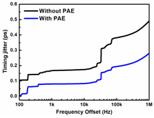
After initiating the PAE, the
uncorrelated phase noise contributed by the residual ASE noise of
the RHML-SOAFL is significantly
decreased, which leads to a timing
jitter reducing from 0.5 to 0.28 ps as
shown in Fig. 4. and provides an
amplitude-equalization pulse-train
repeated at 40 GHz to meet the demand of
being a perfect RZ pulsed carrier for
its future application in OTDM network.
Reference: G.
-R. Lin et al., Optics Express, Vol. 18,
No. 9, pp. 9570-9579, Feb. 2010.
|
 |
 |
|
Fig. 1. The
auto-correlation traces of SOAFL at
1st, 5th, 10th,
and 20th RHML orders. |
Fig. 2.
Evolution on RHML-SOAFL spectra at
different RHML orders. |
|
 |
 |
|
Fig. 3. Auto-correlatted
traces of 40-GHz RHML pulse-train
without and with pulse-amplitude
equalization. |
Fig. 4. The
timing jitter of 40 GHz RHML
pulse-train without and with
pulse-amplitude equalization. |
Emitter
Apodization Dependent Angular Luminance
Enhancement of Microlens-Array Film
Attached Organic Light-Emitting Devices
Professor Hoang-Yan Lin
Graduate Institute of Photonics and
Optoelectronics, National Taiwan
University
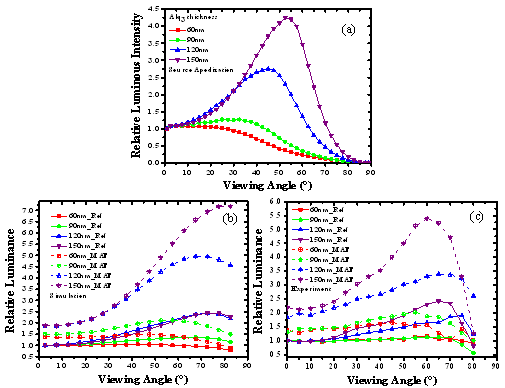
Taking
organic emitter apodization calculated
from electromagnetic theory as input,
the angular luminance enhancement of a
microlens-array-film (MAF) attached OLED
(organic light-emitting device) can be
further evaluated by ray-tracing
approach. First, we assumed artificial
emitters and revealed that not every
OLED with MAF has luminance enhancement.
Then, the OLEDs of different Alq3
thickness were fabricated and their
angular luminance measurement validated
simulation results. Mode analyses for
different layers were performed to
estimate the enhancement potential of
the MAF attached devices. In conclusion,
the organic emitters with higher
off-axis-angle luminous intensity cause
lower out-coupling efficiency but gain
higher enhancement after the MAF
attached.
|
Fig. 1. (a)
The simulated source apodization
varying Alq3 thickness
from electromagnetic theory; (b) the
simulated luminance from geometrical
optics; (c) the validation of
experimental results. |
|
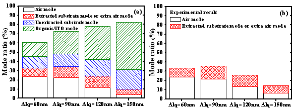
Fig. 2. (a)
Mode ratios calculated by transfer
matrix method with embedded sources.
The blank area of each bar
represented the optical power ratio
of the surface plasmonic mode; (b)
the experimental mode ratios. |
A Novel
Boundary-Confined Method for High
Numerical Aperture Microlens Arrays
Fabrication
Professor Guo-Dung John Su
Graduate Institute of Photonics and
Optoelectronics, National Taiwan
University
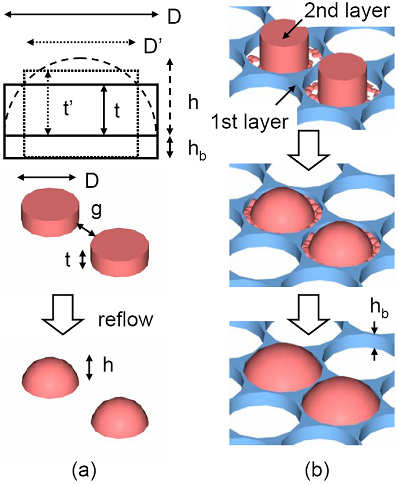
We present a technique to
improve microlens arrays (MLAs)
uniformity after the thermal reflow
process. Microlens arrays (MLAs) usually
form a layered structure in
application-specific optical systems,
such as backlight modules for liquid
crystal displays (LCD), extraction
improvement film for layered light
emitting devices, wavefront sensors,
image recorders, and a focusing
component in the optical communication
devices. It is hard to make small lenses
and large arrays by traditional
machining. Although several methods are
proposed to replace the traditional
machining, thermal reflow process is
widely used to fabricate MLAs.
To
overcome this difficulty, a novel method
is proposed and demonstrated in this
paper. It is called the
boundary-confined method. A boundary
between each PR cylinder is defined
first by a thin negative tone PR. A
thermal reflowing of a 2nd
thick PR is halted at the boundary, as
shown in Fig. 1. The uniformity can be
improved without the cling phenomenon.
Besides, the boundary is narrow and only
a small amount of fill-factor is
sacrificed. The height of the microlens
is adjustable by the different diameter
of PR cylinders inside the same boundary
wall. We achieved high uniformity and
high-NA (numerical aperture)
simultaneously without sacrificing
fill-factor too much. In order to
improve fill-factor, residual PR (photoresist)
between the photoresist cylinders are
used to make photoresist flow outward in
standard thermal reflow processes. PR
cylinders, however, merge together
easily due to an inexact reflow time and
temperature distribution. This results
in low uniformity and small lens height
or low-NA. We proposed a
boundary-confined method to pattern thin
PR holes to prevent PR microlenses from
merging together even after a long
reflow time. Thick PR cylinders are
patterned inside thin PR holes served as
boundaries. PR microlenses are formed
after reflowing the thick photoresist
cylinders. Both the uniformity and the
height of microlens can be well
controlled. Besides, the fill-factor is
high due to the high resolution at thin
photoresist layer in photolithography.
Our results show that the microlens is
approximately a hemispherical profile.
The gap between microlenses with 48
mm
diameter in hexagonal arrangement is 2
mm
and the height of microlens is 22
mm,
as shown in Fig. 2. This work is also
patterned under US 7,713,453 B2.
|
 |
|
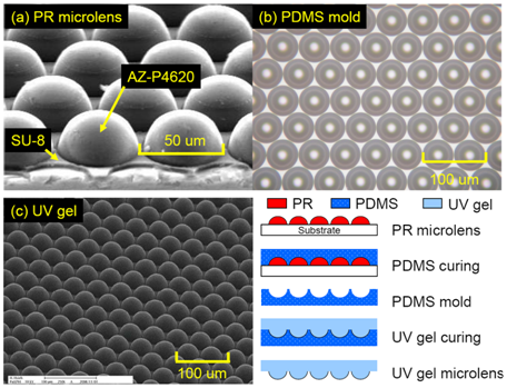
Figure 1.
Schematic drawing of PR reflow by
boundary-confined method. |
|
Figure 2. The
fabrication process sequence, and
(a) PR microlens and SU-8 boundary,
(b) PDMS mold captured by a
microscope, (c) UV gel MLAs after
releasing from PDMS mold. |
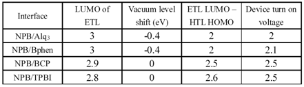
The
Correlation of Turn on Voltage and Band
Alignment in Organic Light Emitting
Diodes
Professor Chih-I Wu
Graduate
Institute of Photonics and
Optoelectronics, National Taiwan
University
Turn on
voltage in the current density-voltage
characteristics is one of the important
factors to evaluate the performance of
organic light emitting diodes (OLEDs).
We report investigation of the origins
of turn-on voltage, defined at where log
J (current density) has a sharp rise and
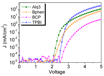
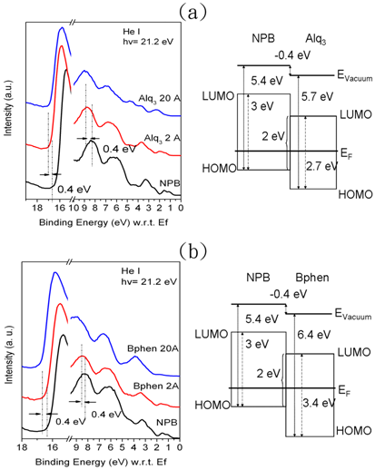
starts to increase dramatically. In
OLEDs with NPB as the hole transport
layer (HTL) and Alq3
as the electron transport layer (ETL),
we find that the turn on voltage is
always at 2V, regardless the cathode
structures being used, such as Ca, Al,
LiF/Al and Cs2CO3/Al.
The turn on voltage is also independent
on the thickness of organic layers
(thickness varies from 30nm to 120 nm).
Beside NPB and Alq3,
we also study the J-V characteristics on
various OLEDs with T3/Alq3,
NPB/T3,
and NPB/Bphen as HTL/ETL, respectively.
In all the devices mentioned above, the
turn on voltage just equals to the
difference between the LUMO of ETL and
the HOMO of HTL, taking into
consideration of vacuum level shift at
organic interfaces measured from the
ultraviolet photoemission spectroscopy
(UPS). Combined with J-V characteristics
of OLEDs and UPS measurement, we
conclude that the turn on voltage of
organic light emitting devices is
determined by the difference between
LUMO of ETL and HOMO of HTL and is
independent of the cathode and thickness
of organic layers. We also found that
the charge transfers at the interface of
ETL/HTL play an important role to the
turn on voltage of OLEDs.
Emitting
Layer Thickness Dependence of Color
Stability in Phosphorescent Organic
Light-Emitting Devices
Professor Jiun-Haw Lee
Graduate Institute of Photonics and
Optoelectronics, National Taiwan
University
We
investigated the strong influence of the
thickness of iridium(III)bis[(4,6-difluorophenyl)
-pyridinato-N,C2’]picolinate
(FIrpic) doped N,N’-dicarbazolyl-3,
5-benzene (mCP) blue emitting layer (B-EML)
on color stability. The large voltage
drop across the B-EML resulted in a
higher sensitivity of the carrier
transport and injection properties to
the applied external voltage. According
to carrier mobility measurements by the
time-of-flight method, the electron
mobility of the mCP exhibited a strong
dependence on the electric field.
Therefore, at a higher driving voltage,
the more rapidly increasing electron
mobility of the mCP and the decreasing
energy barrier height on the electron
transport path would extend the
recombination zone from the B-EML to the
tris(phenylpyridine)iridium (Ir(ppy)3)
doped mCP green emitting layer (G-EML)
in devices with thinner B-EMLs. Coupled
with the fluctuations of the
recombination zone, stronger
triplet-triplet exciton annihilation
occurring in the thinner B-EMLs led to
an even more evident deterioration of
the color stability. After circumventing
these two negative factors, a green-blue
organic light-emitting device (OLED)
with ultra-high color stability was
demonstrated, with the CIE coordinates
slightly shifted from (0.256, 0.465) to
(0.259, 0.467) with increased luminance
from 48.7 to 12700 cd/m2.
Further adding a red phosphorescent
dopant into this green-blue EML
backbone, we successfully fabricated a
white OLED with high color stability,
which exhibited a nearly invariant CIE
coordinate throughout the practical
luminance range from 1050 ((0.310,
0.441)) to 9120 cd/m2
((0.318, 0.446)) and maximum
efficiencies of 26.4 cd/A and 19.8 lm/W
[published in Org. Electron. 11,
1500, 2010].
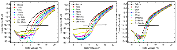
Effects
of Gate Bias and Thermal Stress on ZnO
Thin Film Transistors
Professor
Jian-Jang Huang
Graduate Institute of Photonics and
Optoelectronics, National Taiwan
University
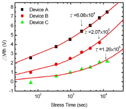
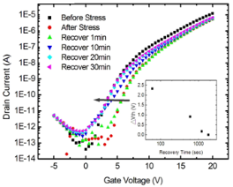
The
effects of gate bias and thermal stress
on the threshold voltage shift were
examined for ZnO TFTs fabricated on the
glass substrate. We compared three
samples with various post ZnO growth
annealing durations. The results show
that the threshold voltage shift (ΔVth)
is only 2.2V after a 1.3×10⁴s
stress at the gate bias 20V for device
C. And the threshold voltage shift can
be correlated to the stress time
following the charge trapping mechanism.
The characteristic trapping time
τ
of device C was calculated to be 1.26×10⁶
s. Further comparisons of the trap
states and off currents reveal that
device C has a better ZnO crystalinity
and a better ZnO/SiNx
interface quality. Finally, the
characteristic trapping time was
extracted at different temperatures for
device C. We obtain an average effective
energy barrier Eτ
of 0.57eV. The results presented in this
work suggested that excellent
τ
and Eτ
can be obtained from ZnO TFTs on the
glass substrate following our
fabrication steps.
|
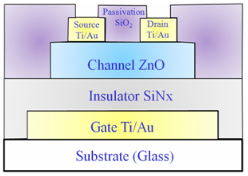 |
Fig. 1: Layer
structure of the ZnO TFT on the
glass substrate.
Fig. 2:
Transfer curves at different stress
time for device A(a), B(b) and C(c).
The bias gate voltage is 20V.
Fig. 3: Time
dependent ΔVth of device
A, B and C under a gate bias 20V.
Fig. 4: Time
evolution of transfer curve during
the recovery phase of device C. The
inset shows the ΔVth
versus relaxation time. |
|
Fig. 2(a) |
Fig. 2(b) |
Fig. 2(c) |
|