|
September 2009 - November 2009 |
| |
|
|
 |
|
 |
| |
Publisher:
Chairman Sheng-Lung Huang Editors:
Prof. Jui-che Tsai, Ms. Hsiao-wen Lin January 15,
2010 |
| |
|
 |
|
Congratulations! Dr. Tingye Li,
Distinguished Chair Professor of GIPO
and Academician of Academia Sinica, receives the IEEE top honor gold medal.
The
Institute of Electrical and Electronic
Engineers (IEEE) awarded its top honor
gold medal to our Distinguished Chair
Professor, Academician Tingye Li,
honoring him for his extraordinary
contributions to fiber-optic
communication technology.
Congratulations on this great
achievement!
Congratulations! GIPO Professor
Hung-Chun Chang receives the title of
“2010 OSA Fellow”.
Congratulations! GIPO Professor
Ching-Fuh Lin receives the 2009
Outstanding Electrical Engineering
Professor Award from the Chinese
Institute of Electrical Engineering.
|
|
 |
|
 |
|
| |
|
|
|
August
“Photonics Forum”
Lecture Highlights |
|
|
August 26th (Wednesday),
2009 10:30 AM |
|
Speaker: |
Prof. Roel
Baets
(Department of Information
Technology, Ghent University) |
|
Topic: |
Silicon Photonics:
Opportunities and Challenges |
| |
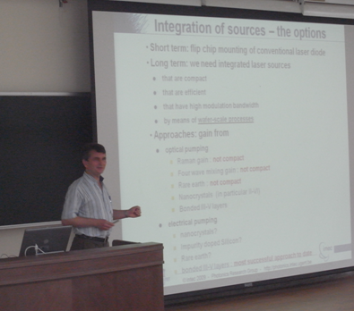
Professor Roel Baets visited GIPO on
August 26th (Wednesday),
2009, and lectured in Auditorium
105, EE Building 2. The lecture,
“Silicon Photonics: Opportunities
and Challenges” was attended with
enthusiasm by GIPO professors and
students, and everyone learned much
from the lecture. |
|
 |
|
October
“Photonics Forum”
Lecture Highlights |
|
|
October 23rd (Friday),
2009 2:30 PM |
|
Speaker: |
Prof. Ray-Kuang
Lee
(Institute of Photonics
Technologies, National Tsing Hua
University) |
|
Topic: |
Light localization in
classical and quantum worlds |
| |
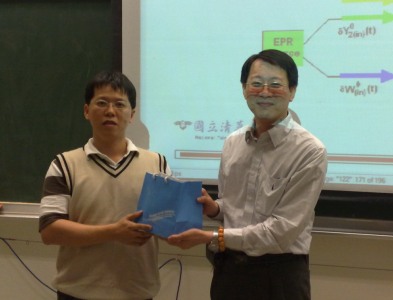
Professor Ray-Kuang Lee visited GIPO
on October 23rd (Friday),
2009, and spoke in Room 113, Barry
Lam Hall. His lecture, “Light
localization in classical and
quantum worlds” was attended with
enthusiasm by GIPO professors and
students, and everyone learned a
lot. |
|
 |
|
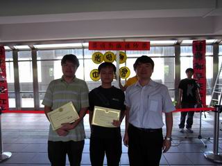
Vice Chairman Gong-Ru
Lin (right), the host, and Professor R.
K. Lee (left) |
|
|
October 30th (Friday),
2009 2:30 PM |
|
Speaker: |
Prof. Chii-Chang
Chen
(Department of Optics and Photonics,
National Central University) |
|
Topic: |
My France Dream - my
experiences in French life, culture,
and study |
| |
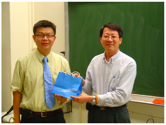
Professor Chi-Chang Chen visited
GIPO on
October 30th (Friday),
2009,
and spoke about his France dream,
his experiences in French life,
culture, and study, at room 113,
Barry Lam Hall. Chii-Chang Chen is a
professor of the
Department of Optics and Photonics,
National Central University. In his
youth, he gave up his original plan
of studying in the U.S., and went to
France instead to pursue further
study. Living in a non
English-speaking country for 5
years, the experience of life and
the culture shock have greatly
augmented his physical and spiritual
strength. He believes that if one
has a dream and pursues this dream
earnestly, one is successful
regardless of whether the goal of
the dream has been achieved. GIPO
students and teachers attended the
speech with enthusiasm, and have
benefited greatly. |
|
 |
|
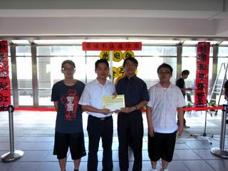
Vice Chairman Gong-Ru Lin
(right), the host, and Professor
Chii-Chang Chen (left) |
~ Series
Report of the 1st Microstructure
Photography Contest 2009 ~
(Date of
judging: August 17th, 2009; location:
B1, Barry Art Gallery, Barry Lam Hall, NTU)
29 photos went into the finals of GIPO’s
1st Microstructure Photography Contest.
They were exhibited at the Barry Art
Gallery of Barry Lam Hall B1 for the
finals on August 17. The photographers
were invited to explain and discuss
their work at the showing. Afterwards,
the judges convened and, after a series
of fervent discussion and appraisals,
announced the results. All winning
photos were displayed at the gallery,
and published in succession in the GIPO
newsletter. This way, those who were
unable to visit the exhibition can still
appreciate the brilliance of these
photos.
|
《Best》
【Title】Summer
Snow
【Photographer】Yi-Hao
Pai, Chih-Hsien Cheng, and Chung-Lun Wu |
|
 |
|
《Excellent》
【Title】Man's
World
【Photographer】Po-Chun
Yeh |
|
 |
|
《Excellent》
【Title】Flame
of Flowers
【Photographer】Chieh-Wei
Huang |
|
 |
|
《Good》
【Title】It
Seems that a Nanometer Granule has a
Life of Its Own
【Photographer】Ting-Ta
Chi |
|
 |
|
《Good》
【Title】
A Grain of Sand, A World
【Photographer】Szu-Yu
Chen |
|
 |
|
《Good》
【Title】Luxuriant
Branches and Leaves
【Photographer】Shu-Ting
Kuo |
|
 |
|
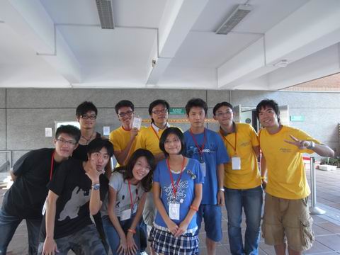
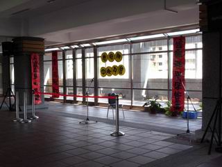
~2009
Academic Year GIPO Students'
Association Mid-Autumn Festival
Party ~
(Time:
September 25th, 2009; Location: 3F
Courtyard, Ming Da Hall, EECS NTU)
Composed by: Hsiang-Chun Wei,
President of GIPO Students'
Association
We are thrilled at the success of
this year's Mid-Autumn Festival
party. Did you all have a good time
eating, chatting and receiving
prizes? Thank you all for your
participation, which has made this
event more wonderful. And, we thank
you for your forbearance if there
were any flaws or problems we
overlooked.
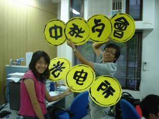
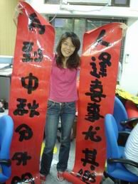
To begin with, I would like to
explain our efforts in preparing
this event. I believe everyone has
noticed that we went the extra mile
with decoration this year. Visually
we had 3 pairs of large-scale spring
festival scrolls written with large
soft pens, the main sign with 7
painted moons, lanterns at the
entrance, and couplets written by
professionals using a writing brush.
For your listening enjoyment, we had
special Taiwanese background music
which, we believe, greatly enhanced
the atmosphere of Mid-Autumn
Festival. In advertising, we had
beautiful posters,
specially-designed meal tickets, and
special drink tickets. In order to
avoid “only early birds getting the
worm”, we prepared a Pizza Hut's
individual pizza for everyone. There
was also a limited amount of special
drinks (which allowed us to discover
quite a few alcoholics), and a
buffet. We prepared so much food
that we were able to fill everyone's
stomach.
|
 |
 |
|
Stage
decoration |
Delicious food
and a flood of revelers |
When it was time for the climactic
lottery, everyone was given a moon
cake for the occasion, which was
purchased from Yu Jen Handicapped
Training Center. So, each time you
take a bite of this moon cake, you
know you have done something good.
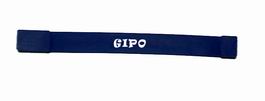
Regarding lottery prizes, we had 50
customized, bracelet flash drives
printed with "GIPO" which, we
believe, are memorable, and classy
souvenirs. We would like to give our
special thanks to Chairman Jenn-Gwo
Hwu, Department of Electrical
Engineering, for his kind donation
of valuable Sogo gift certificates
for our prizes. As we wanted to have
prizes available for almost
everyone, our prizes may not have
been as valuable as those of the
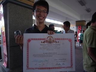
years past. A special point of
interest is that, for the first 3
prizes, we also presented pomelos
bearing professors' signatures and
enlarged “Usavich
Diplomas.”
|
 |
 |
|
Time for the
Mid-Autumn Party lottery |
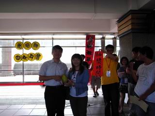
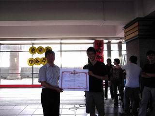
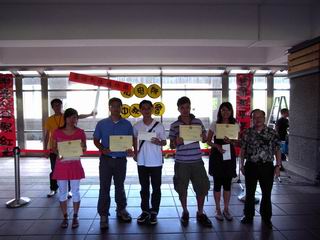
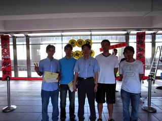
In addition, the winners of GIPO's
2009 1st Microstructure Photography
Contest were awarded during the
party. Since every winner tried the
best to shoot his/her award-winning
photo, we wanted to take this
opportunity to introduce them to you
all.
|
 |
 |
|
Awarding
ceremony of the 1st Microstructure
Photography Contest |
 |
 |
|
Awarding
ceremony of the 1st Microstructure
Photography Contest |
We would like to thank the
Chairman of GIPO, the Vice Chairman
and all the professors for their
participation. Also, thank you to
Professor Jenn-Gwo Hwu, Chairman of
the Department of Electrical
Engineering, for his participation
and gift certificates. Their
assistance has made this party
complete and more successful. Thanks
to the staff of GIPO and offices of
EE Building 2, Barry Lam Hall, and
Ming Da Hall for their support and
assistance. Lastly, we would like to
thank our working staff, Chia-Nying
Hu, Yi-Wen Wang, Je-Yu Chang, Jay-Zway
Hong, Yen-Liang Liu, Yun-Chi Lee,
Yu-Ting Hong, Po-Yu Lin, Shu-Han
Hsu, and Hsiao-Yuh Wang, for their
hard work in making this event
possible. Also, to those special
friends who contributed help without
receiving prior notice from us,
thank you.
|
|
|
|
|
|
| |
|
|
~ 2009 Academic
Exchange with Nanjing University Ph.D. Students ~
Time:
July 5th ~ 11th, 2009
Location: Nanjing University
Composed by Tzu-Huan
Cheng, GIPO Ph.D. candidate (Deputy Team Leader of NTU
representative student team)
The time for visiting Nanjing University drew closer and
closer with each of the several preparatory meetings we held. I was made
a bit nervous by the warnings we had received in our meetings, such as
to avoid mentioning politically sensitive topics, to understand Nanjing
University's research facilities or related geographical and historical
background, etc. Upon arriving in Nanjing and passing through customs,
we received a warm welcome from Nanjing University’s representatives,
and after the next 6 days of interaction and exchange, we realized that
they are in fact very friendly.
During the few days of the seminar, I was deeply moved
and inspired by both the professors' lectures and the students' research
reports. From the amazing lectures of Professor C. C. Yang, former
Chairman of GIPO, Professor Min Xiao, Nanjing University, and Professor
and Academician Jianquan Yao, Tianjin University, we learned a lot about
the many applications of near-field optics to light-emitting devices,
the optical characteristics of nanocrystalline silicon and
microstructure, and the development of THz technology and its
application to communication. We were especially moved by the elderly
Academician Jianquan Yao. Even though he looked tired after having just
flown to Nanjing, his determination to educate us was not a bit
affected. The professor gave us a lecture without a moment's rest, with
enthusiastic participation from the attending students. Although their
fields of study may differ a bit, each student’s determination to pursue
knowledge is apparent and the same. Such a positive attitude towards
research is truly worth studying.
Students from NTU, Nanjing University, and other Mainland
Chinese universities then presented their papers, and some of them also
presided at the sessions. Through presiding, we gained and practiced the
skills of controlling session times, meeting contingencies, and
developing proper conference etiquette. There were 4 major topics in
this seminar: 1. nonlinear optics and laser technology, 2. nanophotonics
and artificial band gap material, 3. wide band gap semiconductor
materials and their microstructure, and 4. new optical effects of
microstructure materials. Oral reports were all made in mandarin. Thus,
aside from some translative technological terms, listeners had basically
no problem understanding each speaker. Among these topics, the ones
discussing wide band gap semiconductor materials and the new optical
effects of microstructure materials incited the most enthusiastic
discussions. In these two topics, papers covering microstructure process
(nanowire, photonic crystal, nanoparticle and quantum well), material
characteristics (silicon nanowire, gallium nitride nanowire, ZnO
nanoparticle, aluminium nitride, and aluminium gallium nitride) and
simulations (the energy band structure calculations and optical
characteristics of the nano materials, negative refraction of materials,
the band-gap changes and reflection characteristics of photonic
crystals), were presented. With fervent discussions, everyone learned a
lot. Among them, I was most impressed by the simulations discussion.
Most students could in fact write their own simulation programs, instead
of relying on commercial software packages. They were also able to
discuss and explain their simulation program writing skills. These
indicate that they already had thorough knowledge of the physical
phenomena of the device materials. In the discussion, Chuan Zhang, a
Nanjing University student, presented an important concept which asserted that, in predicting
material characteristics based on physical models, every theory has to
be verified by experiments before it could possibly be concluded.
Whenever a discrepancy is detected, further verification is needed. Many
discoveries were found from such further verification. Lots of great
discoveries had actually been observed before they were really noticed;
some researchers may have missed receiving the Nobel Prize because of
their neglect of some minor discrepancies.
Finally, I would like to discuss my thoughts about this
academic exchange. I believe this kind of activity is very valuable,
because it not only broadens our fields of vision and provides us with
access to different points of view, but also diversifies our own
viewpoints and prevents us from confining ourselves to our own domain.
The application value of our research would certainly increase greatly
if we bring knowledge of other domains into ours. Seeing the rapid
growth of Nanjing has greatly changed our limited impression of the
city. We need to strive harder to increase our abilities and value and
let foreign friends have more opportunities to get to know us. This way,
we are visiting foreign countries, and in addition, creating
opportunities for foreigners to visit us as well. I hope such activities
can continue, and even expand to a larger scale, so that future GIPO
students can have such seminars and such opportunities for academic and
cultural growth as we do today.
|
|
|
|
|
|
|
| |
|
|
|
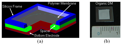
Miniature optical
autofocus camera by micromachined
fluoropolymer deformable mirror
Professor Guo-Dung Su
Graduate Institute of Photonics and
Optoelectronics, National Taiwan
University
Along
with the progress of image sensors in
recent years, fix-focus cameras on
mobile electronic devices do not fulfill
consumer needs. With the size of mobile
devices getting smaller and smaller, the
displacement-to-thickness ratio is
getting larger, and that makes
mechanical motor systems difficult to be
packaged inside cameras to achieve
autofocus function.
We
propose a design using micromachined
fluoropolymer deformable mirrors rather
than traditional mechanical motor. With
low color dispersion and adjustable
power range of 20-diopter, deformable
mirrors can be integrated into optical
module and are well suitable for
miniature optical auto-focus camera. A
polymer membrane works as a reflective
mirror surface to focus the light
variably by adjusting the voltage
difference. Fig. 1 shows a schematic
drawing and photograph of the fabricated
device.
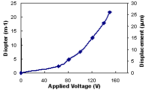
We
conducted an experiment between optical
power versus applied voltage. The
polymer membrane was actuated by the
electrostatic force and deformation of
the polymer membrane can be adjusted by
changing voltage difference
continuously. The optical power and
deformation versus the applied voltage
is plotted in Fig. 2. The maximum
optical power achieved is around
20-diopter when 160 volts is applied,
corresponding to 27-μm deformation at
the center of the membrane. The optical
power of an organic deformable mirror
could be adjusted continuously.
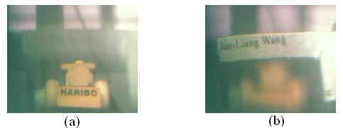
At the beginning, when
the mirror was not actuated, the far
object (the train) with “HARIBO” can be
seen clearly while the near object, the
name card with “Jen-Liang Wang”, is
blurred as show in Fig. 3(a).
After applying voltage to the deformable
mirror, the effective focal length of
the system changes. The focal point
moves forward so that the near object
can be clearly seen. We can see that
there are still some aberrations at the
edge of the images. This can be fixed by
custom-designing the lenses. We
demonstrate that the deformable mirror
is feasible as vari-focus devices in
camera lens module without moving
component. This part is also shown in
the video file submitted.
|
 |
|
Fig. 1. (a) A
schematic drawing of organic deformable
mirror and (b) a photograph of the
device. |
|
 |
|
Fig. 2. Optical
power versus applied voltage. |
|
 |
|
Fig. 3. (a) Image
for system without actuating deformable
mirror, and (b) image when performing
auto-focusing, the mirror is actuated. |
White Organic Light-Emitting Devices
with Low Driving Voltage and High
Efficiency
Professor Jiun-Haw Lee
Graduate Institute of Photonics and
Optoelectronics, National Taiwan
University
By
selectively doping yellow emitter in the
ambipolar blue emitting layer (EML),
white light organic light-emitting
device (OLED) could be obtained and the
driving voltage was reduced due to the
recombination current increase. We doped
rubrene near the maximum recombination
zone of our OLED,
4,4'-bis[2-(4-(N,N-diphenylamino)phenyl)vinyl]biphenyl
doped in 9,10-bis(2’-naphthyl)
anthracene (DPAVBi:ADN), 2V reduction in
driving voltage was achieved. Although
electron and hole mobilities of ADN are
comparable, we found the recombination
zone is near the interface of
hole-transport layer (HTL) and EML
interface the injection barrier for the
hole is higher than that for the
electron.
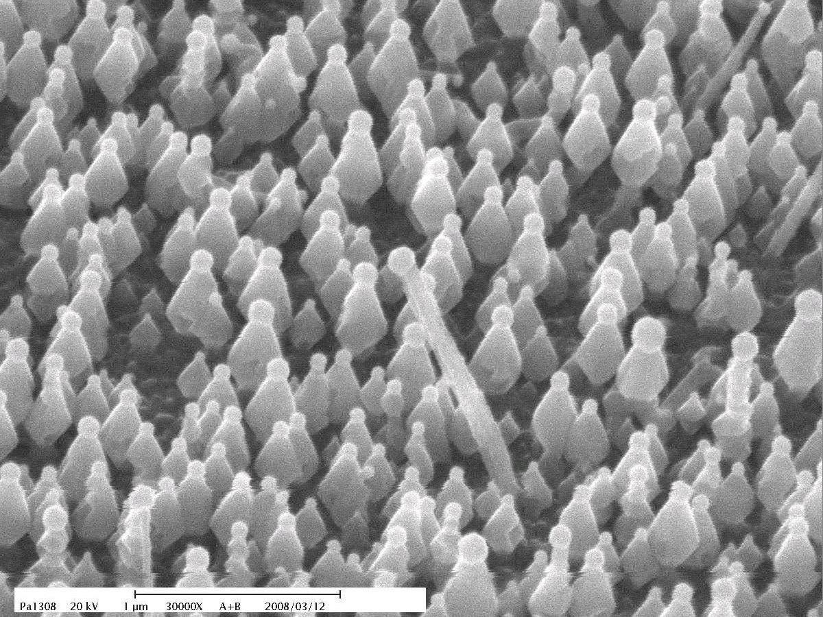
Characterizations of GaN-Based LEDs
Encompassed with Self-Aligned Nanorod
Arrays of Various Distribution Densities
Professor Jian-Jang
Huang
Graduate Institute of Photonics and
Optoelectronics, National Taiwan
University
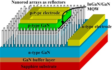
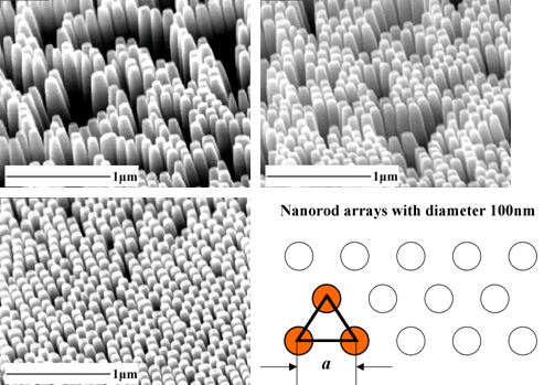
GaN-based LEDs
encompassed with self-aligned nanorod
arrays of three types of nanorod
arrangement were fabricated by simply
using spin-casting and dry etching.
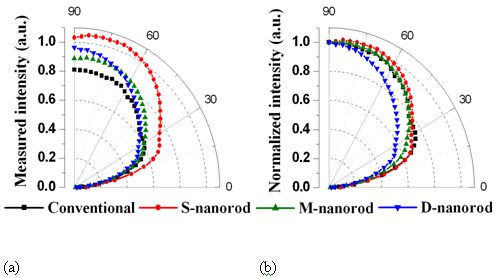
Light diffraction behaviors are
characterized by considering the
radiation profiles of these structures.
The output power enhancement factor of
the S-nanorod device over the
conventional one is 27.25% in the
vertical direction and 30.43% for the
integrated intensity. This
enhancement is omni-directional because
the less regular arrangement of S-nanorod
structure results in a varying
G
and omni-directional distribution of
radiation modes. On the other
hand, from the radiation profile, the D-nanorod
device shows better directionality due
to its relatively well-aligned nanorod
arrays (and thus less varying lattice
vector
G)
but with a less optical output
enhancement. The relatively
well-arranged D-nanorods, especially in
the first several columns facing p-mesa
act as gratings with groove in the
vertical direction and diffract
laterally propagated light back toward
the p-mesa, thus decreasing the amount
of power enhancement. Also, the
existence of higher order diffraction
modes enables the S-nanorod device to
have a higher power enhancement factor.
|
 |
|
Fig. 1.
Illustration of the LED device
encompassed with nanorod reflectors |
|
 |
|
Fig. 2. SEM photos
of the self-aligned nanorod arrays of
the (a) S-nanorod, (b) M-nanorod, and
(c) D-nanorod LEDs. The fill
factors are 0.188, 0.285 and 0.467 for
(a), (b), and (c), respectively.
(d) Illustration of the triangular
lattice for the calculation of the
effective lattice constant
a
for a specific fill factor. |
|
 |
|
Fig. 3. Measured
radiation profiles (a) and the
normalized results to the vertical
direction (90˚) (b) of the devices under
comparison. |
Analysis
of Highly Conducting Lamellar Gratings
with Multidomain Pseudospectral Method
Professor Yih-Peng
Chiou’s group
Graduate Institute of Photonics &
Optoelectronics, National Taiwan
University
Numerical modeling for grating
structures plays an important role in
their investigation and applications.
The performance of the modeling is even
essential, when grating periods become
comparable to the wavelength and
structures are involved with highly
conducting materials. The rigorous
coupled wave analysis (RCWA) is the most
widely used spectral methods. But in
recent years, numerical instability
problem with TM polarization was
discovered when the real part of the
refractive index is very small (highly
conducting gratings). Another common
modal method is the classical modal
method which is very powerful technique
to approach this problem, but its
complicate process to limit the further
applications. Here we combine the
features of these two numerical methods:
the easily solved eigen equation in the
grating of RCWA and the analytical mode
profiles of modal method. The
multidomain pseudospectral frequency
method we adopted avoids classical modal
methods from finding the roots of
dispersion relation especially while
complex roots are involved and avoids
Runge phenomenon and Gibbs phenomenon to
achieve uniform accuracy at the same
time.
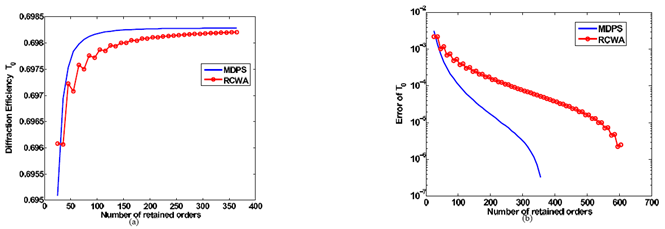
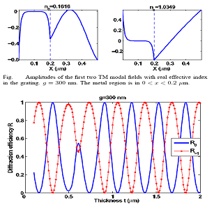
The validity of numerical results by
MDPS is compared with commonly used
rigorous coupled wave analysis for TM
polarization. The numerical evidence
shows the developed method has not only
better stability but also higher
efficiency.
|
 |
|
Fig. 1. Simulation
results of a metallic lamellar grating
of pitch 0.25μm with index 3.18-4.41j
deposited on glass substrate with
TM-polarized wave 0.55μm. (a) The
diffraction efficiencies T0 by RCWA and
MDPS. The circle line is obtained by
using RCWA, and the solid line by MDPS.
(b) The retained orders dependence of
convergence of diffraction efficiencies. |
|
 |
 |
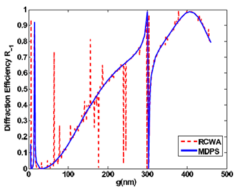
|
Fig. 2.
Diffraction efficiency R−1
of a highly metallic lamellar
grating of pitch 0.5μm with index
-10j as the function of the groove
width g. The wavelength is 632.8 nm.
The solid curve is obtained by MDPS
and the dash line by RCWA. |
Fig. 3. (a)
Amplitudes of the first two TM modal
fields with real effective index in the
grating. (b) Numerically calculated
diffraction efficiencies as a function
of grating thickness. |
Y.-P. Chiou, W.-L.
Yeh, and N.-Y. Shih, IEEE/OSA Journal
of Lightwave Technology, 27,
Dec. 2009.
Experimental characterization of
two-axis MEMS scanners with hidden
radial vertical combdrive actuators and
cross-bar spring structures
Professor Jui-che Tsai
Graduate Institute of Photonics and
Optoelectronics, National Taiwan
University
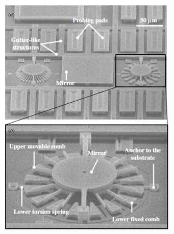
We
perform the experimental
characterization of two-axis MEMS
scanners driven by radial vertical
combdrive actuators (Figure 1). The dc
scan ranges are limited by the pull-in
effect. Each scanner utilizes a
cross-bar spring structure to achieve
two rotational degrees of freedom (DOFs)
without employing any gimbal. Both the
actuators and torsion springs are hidden
underneath the mirror to obtain a small
form factor. The devices are fabricated
by a five-layer polysilicon surface
micromachining process (SUMMiT-V).
Devices with different combinations of
parameter values are experimentally
characterized and compared.
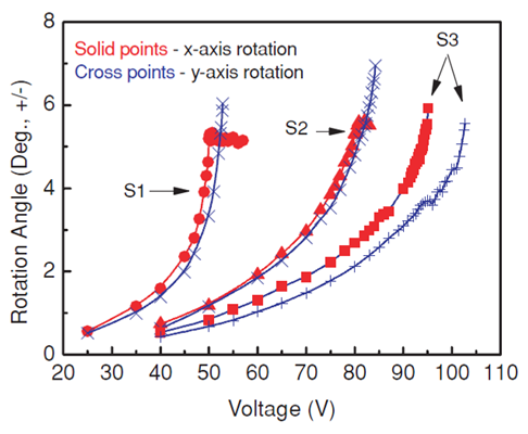
The
optimal design (S1) comes with a
balanced cross-bar spring structure. The
mechanical rotation angles are ±5.30°
(50.2V) and ±6.04° (52.8V) for rotations
about the x and y axes, respectively
(Figure 2). For each rotational mode, a
significant angle is obtained under a
reasonable bias voltage. The resonant
frequencies are 11.4 kHz and 11 kHz.
|
 |
|
Figure 1 (a) SEM
photo of typical devices and (b) a
close-up of the device with a circular
mirror. |
|
 |
|
Figure 2
Comparison between the dc
characteristics of three devices with
balanced cross-bar spring structures. |
© 2009
Institute of Physics (IOP) and IOP
Publishing Ltd
J. C.
Tsai et al., “Experimental
characterization of two-axis MEMS
scanners with hidden radial vertical
combdrive actuators and cross-bar spring
structures,” J. Micromech. Microeng.,
Vol. 19, No. 4, 045002, Apr. 2009.
|
|
|
|
|
|
| |
|
|
 |
|
 |
|
|
|