|
|
 |
|
 |
| |
Publisher:
Chairman Sheng-Lung Huang Editors:
Prof. Jui-che Tsai, Ms. Hsiao-wen Lin September 30,
2009 |
| |
|
 |
|
May
“Photonics Forum”
Lecture Highlights |
|
|
May 1st (Friday),
2009 2:30 PM |
|
Speaker: |
Prof. Gavin Conibeer (University of
New South Wales, Australia) |
|
Topic: |
Third Generation
Photovoltaics |
| |
Prof. Gavin Conibeer visited GIPO on
May 1st (Friday), 2009,
and lectured in room 105, the EE
Building II. His lecture, “Third
Generation Photovoltaics” elicited
enthusiastic participation from GIPO
professors and students, and
everyone learned much. |
|
 |
|
Workshop |
Workshop on Display,
Lighting, and Solar Cell
Optoelectronics Technologies |
|
Time: |
May 8th (Friday),
2009 10:00 AM ~ 5:50 PM |
|
Speakers: |
Deputy Director Chien-Jen
Sun (Electronics
& Optoelectronics Research
Laboratories, Industrial
Technology Research
Institute)、Professor Jian-Jang
Huang (GIPO)、Professor Guo-Dung
Su (GIPO)、Professor
Hoang-Yan Lin (GIPO)、Professor
Ching-Fuh Lin (GIPO)、Director
Chung-Wen Lan (Photovoltaics
Technology Center,
Industrial Technology
Research Institute) |
|
Presiders: |
Professor C. C. Yang,
Professor Hung-Chun Chang,
Professor Jian-Jang Huang,
Professor Lung-Han Peng |
|
Attendance: |
95 visitors, 60 GIPO
students |
|
Location: |
Auditorium 101, Barry Lam
Hall, National Taiwan
University |
|
|
The “Workshop on Display,
Lighting and Solar Cell
Optoelectronics
Technologies”, planned by
GIPO professor C. C. Yang,
took place on May 8th in
auditorium 101 of Barry Lam
Hall. From the Industrial
Technology Research
Institute, Director Chung-Wen
Lan of the Photovoltaics
Technology Center and Deputy
Director Chien-Jen Sun of
Electronics and
Optoelectronics Research
Laboratories were specially
invited to speak at this
event. In addition, four
GIPO professors (Professor
Ching-Fuh Lin, Professor
Hoang-Yan Lin, Professor Guo-Dung
Su, Professor Jian-Jang
Huang) also attended as
speakers. Visiting
participants from all over
Taiwan attended the workshop
with enthusiasm. Aside from
GIPO students and
professors, workshop
participants included
directors and research and
development personnel from
the industry, professors and
master and doctoral students
from other schools, and
personnel from research
institutions. This workshop
allowed GIPO professors and
students to better
understand the current state
of this industry and the
direction of future
development. |
|
 |
~ Self Introduction of the 2009-10
President of the GIPO Student
Association ~
Composed
by GIPO doctoral student Hsiang-Chun Wei
(newly
appointed President of the GIPO
Student Association)
Hello everyone, it is an honor to
serve as the President of the
Student Association this year for GIPO professors and students. My
name is Hsiang-Chun Wei, and I am a
3rd year doctoral student, studying
in Professor Guo-Dong Su’s
laboratory. It has been 2 years
since I was admitted into GIPO, and
I have become accustomed to this
environment by degrees. GIPO has the
best teachers, best students, and
best facilities in the country, and
so naturally, concentrating on and
excelling in research is a goal that
we all strive toward. During those
late nights at the laboratory, when
anxiety causes pimples to surface on
your nose, did you wish that life
could be a little more fun and
exciting? Have you overlooked the
beauty of nature when you are buried
under piles of journals? During this
one year's term, I would like to
bring some amusement to the lives of
my fellow classmates.
Please allow me to introduce to you our
capable
vice-president
Jay-Zway Hong, with whom I’m
thrilled to work with. He is a
2nd-year master student, studying in
Professor Ming-Hua Mao's laboratory.
Jay-Zway is a man of
enthusiasm with a sense of
responsibility and also a sense of
humor. With such a strong team, we
will work hard to serve you
efficiently in building friendships
among students, among laboratories,
and between GIPO staffers and
students.
When I was approached to prepare a self introduction for the GIPO newsletter, I had no idea what
to write. I am not quite an
outstanding researcher, I am neither
well-known nor especially
attractive, and I have no fresh and
creative political views.
Nevertheless, the one guarantee I
can make is that I will be working
to serve you anywhere, anytime, and
that activities and events which
should take place, will take place.
One for all, all for one!
~
Highlights from GIPO's Summer
Photonics Camp, 2009 ~
(Time: July 15th
~ 17th, 2009;
Location: Barry Lam Hall and EE
Building II, National Taiwan
University)
Composed by GIPO
master
student
Jay-Zway Hong
(newly appointed Vice President of
the GIPO Student Association)
Taiwan’s optoelectronics industry is
renowned worldwide, and has become
known as the “Taiwan Miracle”. Many
students have nevertheless wondered
how this industry could thrive
during today's financial crisis. The
challenges and trends of this
industry have been of great
interest. The photonics camp,
held every year by NTU GIPO, enjoys
great popularity among college
students across the country, and
will answer all your questions.
The summer photonics camp has
been a GIPO tradition for years.
Students curious about
optoelectronics gather from
different universities all around
the country to unveil the mysteries
of Taiwan's optoelectronics
industry. With a series of lectures
concerning signal transmission and
processing, display, optical
storage, light-emitting components,
energy, and industrial upgrade; the
camp provides a detailed and
thorough explanation for students.
During the camp, students who are
fascinated by the optoelectronics
industry learned about the most
advanced technological developments
and principals, as well as
information known only to those
inside industrial circles. In these
three short days, students filled
their brain with optoelectronics
knowledge, and their stomach with
delicacies. Then, eager to begin
work and with a sparkle in their
eyes, students returned home and
showed off what they have learned in
the camp, and shared these with
their parents and classmates.
In view of the fact that personal
experience always makes a deeper
impression than lectures, the camp
is designed to provide opportunities
for students to do experiments with
their own hands. During the
afternoon of the first day, we
arrived at an optoelectronics
laboratory at EE Building I. We then
performed three experiments: the
first was to evaluate the yield of
solar cells, the 2nd was using
instruments to evaluate the quality
of projectors, and the 3rd was to
measure the L-I-V curve
(Light-Current-Voltage curve) of a
blue LED and use photo luminance to
obtain the spectral characteristics
of light-emitting components.
Every participating student was
eager to try, and asked many
questions. Everyone was reluctant to
leave when class was over.
|
 |
 |
|
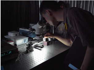
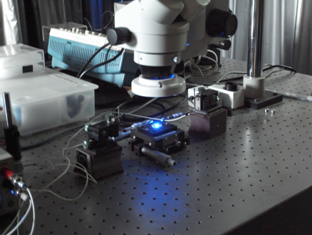
Students carefully use probes
to make measurements |
The awe-inspiring blue light
LED |
After the experiments, we went to
the Demonstration Room of Flat Panel
Display. It's a platform
created by both academia and
industry. The center contains the
most advanced display technology
research and the most
newly-developed materials and
products provided by the leading
companies in this industry. The
students had a lot of fun working
with interactive teaching materials,
and came to understand that the
display device is much more
complicated than its light and
simple appearance implies. In making
display devices, the liquid crystal
type, polarizers, driving circuits,
back light modules, optical system
design, material selection,
fabrication, and packaging all play
important roles.
Visiting laboratories is an
important part of this camp.
Generally speaking, laboratories are
not open for public visitation, as
there are top-secret and hard-won
research results inside. In
addition, the instruments and
equipment are quite valuable; the
instruments in clean rooms alone
could cost tens of million of
dollars. Numerous students wish to
visit the NTU laboratories, yet few
have had their wish granted.
However, through the summer
photonics camp, all participants have
such opportunity. Special thanks to
Professor Gong-Ru Lin, Professor
Lung-Han Peng, Professor Sheng-Lung
Huang, and Professor Jian-Jang Huang
for offering us their laboratories
and laboratory guides. Every
laboratory guide was passionate
about research, energetic, and
knowledgeable, inspiring great
respect and admiration in the
participating students.
|
 |
|
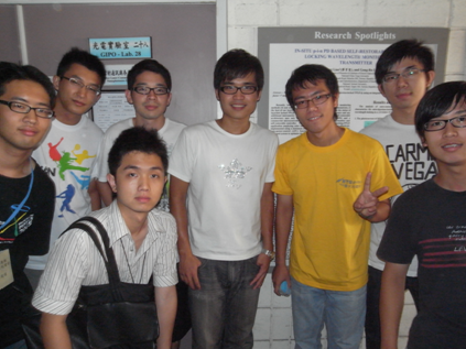
Upper
and lower classmen interacting and
chatting happily |
It has been my honor to take part in
this three day camp. One of the
participants indicated on his
feedback form that he wished to be
admitted to NTU’s amazing and
elegant GIPO next year so that he
could work for this camp together
with me. I was so touched in reading
this that I felt tears came into my
eyes. My endeavors had been accepted
by fellow students, and that was my
greatest gain in running this camp.
|
|
 |
|
 |
|
| |
|
|
~ Symposium and
lecture of Academician Yuan-Tseh Lee (former President of Academia
Sinica) ~
Time: May 15, 2009
Locations: meeting room, 7th floor & Auditorium 101, Barry Lam Hall,
National Taiwan University
In order to give more GIPO students an opportunity to
interact with Academician Lee, former president of Academia Sinica and a
Nobel Prize laureate in chemistry, we invited him, during our interview
with him last September, to speak at our Photonics Forum and share his
insights with us. He accepted our invitation instantly, and after
consulting his schedule, confirmed that he would visit on May 15.
To make the most of this rare opportunity, we arranged a
casual lunchtime exchange between GIPO professors and academician Lee in
the 7th floor meeting room of Barry Lam Hall. 16 GIPO professors
attended with great enthusiasm, and Dean Soo-Chang Pei of College of
Electrical Engineering & Computer Science, was invited to speak at the
beginning of the session. During the exchange, professors asked
Academician Lee to share his insights on various issues, and discuss his
experiences with the dilemma of focusing on research or career
advancement, and difficulties with balancing research and family.
Academician Lee replied to these questions thoroughly, sharing his
thoughts and experiences. The pleasant exchange lasted for one and a
half hours, and both parties wished for more time to talk.
|
 |
|
Academician Lee
and GIPO professors during their
lunchtime exchange |
The Photonics Forum, beginning at 2:30 pm at auditorium
101, Barry Lam Hall, attracted so many EECS students and teachers that
all seats had been taken half an hour before the meeting began. The
topic of the day was "My Research Career". After a short opening speech
delivered by Chairman Sheng-Lung Huang, Academician Lee began sharing
with us his tens of years of research experience and insights. Beginning
with his bachelor thesis, the professor’s thirst for learning and
knowledge has led him through learning how to solve problems, through
how to find his own direction, and through each step toward the summit
of his career. Although receiving the Nobel Prize in Chemistry was quite
an honor, Academician Lee actually finds more satisfaction in leading
the rest of the world in his research fields. After the lecture,
participants raised several types of questions. Academician Lee shared
his insights with attending teachers concerning how to nurture students.
For the students in attendance, he advises that in addition to being
passionate about research, having curiosity, and enduring concentration,
always believing that there is a better solution would be of great
benefit to scientific research.
The lecture lasted for two hours and ended amid eager
applause. Through the rare opportunity of this visit, we learned how
Academician Lee has devoted himself to study, and how he also paid close
attention to other things besides research. It is clear that everyone
has been greatly inspired and has gained a lot of fresh ideas and
inspiration.
|
 |
|
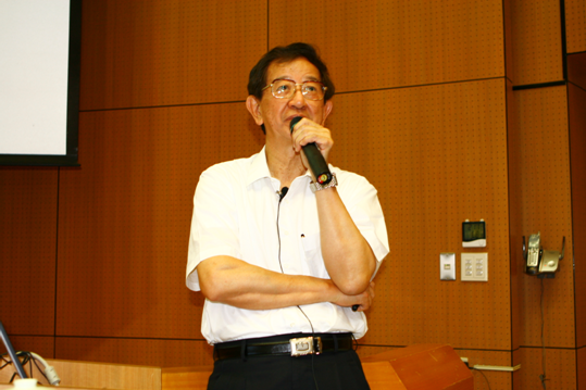
Academician Lee at
the Photonics Forum, speaking of his
career in research |
~ 2009 Academic
Exchange with Nanjing University Ph.D. Students ~
Time:
July 5th ~ 11th, 2009
Location: Nanjing University
Composed by Jeng-Wei Yu, GIPO Ph.D. candidate (Team Leader of NTU
representative student team)
The second doctoral student exchange
between National Taiwan
University and Nanjing University was held in Nanjing, China. GIPO
Chairman Sheng-Lung Huang, Vice Chairman Gong-Ru Lin, Professor
C. C. Yang,
who was invited to deliver a speech, and ten students visited Nanjing
University. I was honored, with the support of other participating
students, to have the privilege of serving as the NTU student leader.
Therefore, in order to thoroughly draft the details of this exchange, I
had talked and exchanged ideas with Kun Tang, the student leader of the
Nanjing team. It was a pleasure to work with him, and I would like to
thank him for his kind assistance in making preparations and in ensuring
that activities proceeded as planned.
The exchange workshop took place on
the 6th
and 7th of July, 2009. The topics explored were numerous and
impressive. They include the four following: quasi-phase-matching
nonlinear optics and laser technologies, nanophotonics and artificial
bandgap materials, wide bandgap semiconductor materials and micro
structures, and novel optical effects in micro structures. Each student
had 15 minutes to introduce his laboratory and explain his research
achievements. The workshop attracted several other students who weren’t
team members to take part in the interaction, which added much interest
to the event. Both parties agreed to deliver reports in Chinese,
therefore, allowing participants to interact more directly and gain a
deeper impression. Each report had aroused animated discussion, which
often continued on even during intermissions and break times. It is
clear from the fervent discussion amongst members of both teams that NTU
and NU are mutually impressed and interested in each other’s research.
During these fantastic two days of exchange, we fully realized
that the Department of Physics of NU has worked hard in research and has
achieved outstanding results. Each of their student representatives has
done some impressive research. We are so glad to have this opportunity
to interact with and to learn from such excellent friends, inspiring us
to work harder and continue to improve ourselves further.
In interacting with mainland Chinese
students, the most sensitive topic is that concerning China and Taiwan.
I believe everyone must be curious about how we handled this situation.
Basically, the NU students generally did not refer to it, and of course,
we did not either. During the exchange, we took special care not to talk
about this issue; otherwise, it could cause a lot of other problems and
make the situation quite unpleasant. Except for this, getting along with
mainland Chinese students was just like getting along with our own
classmates, nothing unusual about it. Another topic that might be of
special interest to everyone is the differences between universities in
China and in Taiwan. It takes mainland Chinese students 3 years to get a
master degree, and another 3 years to get a doctoral degree. However, it
takes Taiwanese students 2 years to get a master degree and 3 to 7
years, depending on how each individual student performs, to get a
doctoral degree. Moreover, I have learned that their master graduates
could earn as much as 5,000 RMB per month if they manage to find a good
job. However, I have also learned that their doctoral graduates could
only earn less than 4,000 RMB monthly if they stay at and work for their
universities as instructors (similar to our assistant professors). This
is quite surprising, since, in Taiwan, a master graduate would have a
difficult time finding a job with a starting salary higher than that of
a doctoral graduate.
Through this exchange, we have gotten
to know the students of Nanjing University, and furthermore, our ten
GIPO students have gotten to know each other better as well. This has
somewhat brought me some emotion. GIPO students are increasing, and yet,
we are only acquaintances, who rarely interact with one another. Perhaps
GIPO could establish a regularly-occurring platform to promote
friendship and exchange among students. Finally, I'd like to take this
opportunity to thank GIPO Chairman Sheng-Lung Huang, Vice Chairman
Gong-Ru Lin, and several other teachers for their assistance in helping
us to complete this significant and meaningful exchange successfully.
The teachers have worked hard during pre-exchange planning and in their
thoughtful guidance during the exchange. We would also like to thank Ms.
Hsiao-wen Lin of the GIPO office for her hard work for this event, which
has thus led to its success. I hope this meaningful exchange can
continue on and allow more and more GIPO students to experience this
event and learn from it.
|
 |
|
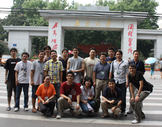
Representative
student teams from both parties in front
of the Nanjing University entrance |
|
|
|
|
|
|
|
| |
|
|
|
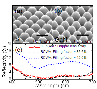
Broad-band anti-reflection effects in self-assembled, subwavelength size of semiconductor nipple array
Professor Lung-Han Peng's group
Graduate Institute of Photonics and
Optoelectronics, National Taiwan
University
We
reported the use of recessive size
reduction in self-assembled polystyrene
sphere mask with anisotropic etching to
form lens-like nipple arrays onto the
surface of silicon and gallium nitride.
These devices are shown to exhibit a
filling factor near to an ideal
close-packed condition and paraboloid-like
etch profile with slope increased
proportionally to the device aspect
ratio. Specular reflectivity less than
3% was observed over the visible
spectral range for the 0.35μm-period
nipple-lens arrays in Fig.1. Using
two-dimensional rigorous coupled-wave
analysis the latter phenomenon can be
ascribed to a gradual index matching
mechanism accessed by a high
surface-coverage semiconductor nipple
array structure.
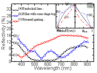
We
further compared the weighted surface
reflectivity of the following surface
textures of (a) paraboloid-like nipple
lens, (b) pillar with a cone-shape etch
top and (c) pyramidal grating using
two-dimensional rigorous coupled-wave
analysis (2D-RCWA). Our calculations
show that the use of structure (a) of
paraboloid-like nipple lens array
renders the lowest reflectivity (<3%)
over the 450-700nm spectral range. The
drastic reduction of reflectivity in the
450-900nm spectral range by texture
change from pyramid to paraboloid can be
ascribed, as referred from the inset of
Fig.2, to a linear change in the
effective refractive profile and thus a
better gradual index matching mechanism
provided by the latter. The oscillatory
behavior of reflectivity in the
450-700nm spectral range of the pillar
structure (b) reveals subtlety of
incomplete destructive interference for
lack of continuous change in the
effective reflective index.
|
 |
|
Fig.1: 0.35μm-period nipple array of (a) Si and (b) GaN showing an aspect ratio of 0.59 and 0.94, (c) Experimental and RCWA-calculated reflectivity spectra for the 0.35μm-period Si nipple array in a near close-packed and non-close-packed condition. |
|
 |
|
Fig.2: Calculated
reflectivity spectra at normal incidence
for surface textures composed of (a)
paraboloid-like nipple lens, (b)
pyramidal grating, and (c) pillar with a
cone shape of etch top over Si. Inset:
surface profile and effective refractive
index profile which are assumed to
reside on a square lattice at a
periodicity of 0.35μm with a filling
ratio~75% and aspect ratio ~0.6. |
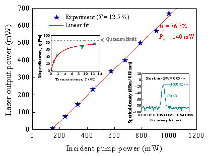
Yb3+:YAG-silica fiber laser
Professor
Sheng-Lung Huang's group
Graduate Institute of Photonics and
Optoelectronics, National Taiwan
University
We demonstrate a compact
continuous-wave
Yb3+:Y3Al5O12–silica
(Yb3+:YAG-silica) fiber laser grown by
the codrawing laser-heated pedestal
growth (CDLHPG) technique. The threshold
is 25 mW, which is an order of magnitude
lower than that of previous short-length
fiber lasers (Yb3+-doped or Er3+/Yb3+-codoped).
A slope efficiency of 76.3% was achieved
from a 7-mm-short Yb3+:YAG-silica fiber,
corresponding to an extracted power of
nearly 1 W/cm. Additionally, low
propagation loss and high emission cross
section have been determined by
analyzing the lasing thresholds and
slope efficiencies, and there is an
excellent agreement between theoretical
results and experimental data.
The
CDLHPG technique provides a simple yet
effective way to incorporate glass
network modifiers (Al2O3 and Y2O3) into
SiO2 host through interdiffusion
process. Further, Cu-Al alloy packaging
is employed to efficiently remove the
heat generated inside the fiber compared
with previous short-length fibers. To
the best of our knowledge, this
7-mm-short Yb3+:YAG-silica fiber laser
with record-low threshold down to 25 mW
and record-high slope efficiency up to
76.3% is the shortest active fiber
reported to date for any short-length
fiber laser operated at room
temperature.
A
68-μm-diameter Yb3+:YAG single crystal
fiber was first grown by the LHPG method
from a 20-mol.% doped <111> Yb3+:YAG
single crystal with a cross section of
500 μm × 500 μm. The as-grown crystal
fiber was then inserted into a fused
silica capillary with 76 and 320 μm
inner and outer diameters, respectively
for redrawing with 5-mm/min growth speed
by the CDLHPG technique. The silica
diffuses completely into the Yb3+:YAG
crystal fiber during redrawing to form
the core of the Yb3+:YAG-silica fiber.
After the CDLHPG process, the as-grown
Yb3+:YAG-silica fiber was packaged by
melting Al at 780 °C in a Cu holder to
make the Cu-Al alloy. Finally, both ends
of the Yb3+:YAG-silica fiber packaged by
the Cu-Al alloy were fine polished for
dielectric coating on the fiber end
faces. The fiber compositions and
microstructure were examined by an
electron probe micro-analyzer and a
high-resolution transmission electron
microscopy, and the refractive index
measurement was carried out by a
home-made confocal microscope using a
635-nm distributed feedback laser. For
laser characterization, the fiber was
excited by a Ti3+:sapphire laser tuned
to 915 nm. Four different output coupler
transmittances of 0.7, 1.7, 8.9, and
12.5% were used for optimizing the
output powers. The pump was first
incident into a standard single-mode
fiber (SMF-28) by a 10X objective, and
was butt-coupled to the core of a
7-mm-long Yb3+:YAG-silica fiber through
a dichroic-coated front face. The fiber
laser output and the residual pump beam
were collimated by an achromatic lens
with 10-mm focal length and further
filtered by a long-wavelength-pass
filter before detection by a photo
detector or an optical spectrum
analyzer.
The performance of the
Yb3+:YAG-silica fiber laser is shown in
Fig. 1. The lasing threshold increases
from 25 to 140 mW as the output coupler
transmittance increases from 0.7% to
12.5%. The maximum output power of 670
mW was achieved with the output coupler
transmittance of 12.5% under 1000-mW
incident pump power, corresponding to a
power yield of ~1 W/cm.
|
 |
|
Fig. 1. Performance of the CW Yb3+:YAG-silica
fiber laser at room temperature. Inset:
the upper one shows the dependence of
slope efficiency on the output coupler
transmittance; the lower one shows the
side mode suppression ratio of ~70 dB at
1-W incident pump power. The gray dashed
and red solid lines are the quantum
limit and the best fit to obtain the
round-trip loss, respectively. |
Aspect Ratio Dependent Ultra-low Reflection and Luminescence of Dry-Etched Si Nano-Pillars on Si Substrate
Professor Gong-Ru Lin
Graduate Institute of Photonics and
Optoelectronics, National Taiwan
University
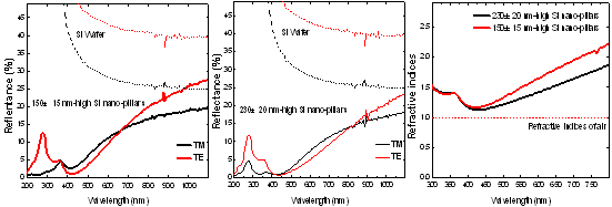
The Si nano-pillars with high aspect-ratio were fabricated by dry-etching the thin-SiO2 covered Si substrate with rapidly self-assembled Ni nano-dot patterned mask (see Fig. 1). Aspect-ratio dependent ultra-low reflection and anomalous luminescence of Si nano-pillar are analyzed for applications in all-Si-based lighting and energy transferring systems. The Si nano-pillars induce an ultra-low reflectance and refractive index of 0.88% and 1.12, respectively, at 435 nm due to the air/Si mixed structure and highly roughened surface. The reflectance can be <10% with corresponding refractive index of <1.80 between 190 and 670 nm (see Fig. 2). Lengthening the Si nano-pillars from 150±15 to 230±20 nm further results in a decreasing reflectance, corresponding to a reduction in refractive index by
Dn/n = 18% in visible and near-infrared wavelength region. After dry etching Si wafer into Si nano-pillars, the weak blue-green luminescence with double consecutive peaks at 418-451 nm is attributed to the oxygen defect (O2-) induced radiation, which reveals less relevance with the ultra-low-reflective Si nano-pillar surface.
|
 |
|
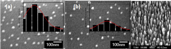
Fig.1 SEM surface morphology of Ni nano-dots after different annealing time at 850
oC
(a) 30 s and (b) 120 s, and SEM surface morphology of Si nano-pillars |
|
 |
|
(a) |
(b) |
(c) |
|
Fig. 2 (a)
and (b) Surface reflectance of Si nano-pillars/Si with high of 150±15 nm
and 230±20 nm,
respectively, and Si wafer (insert) measured by using TM and TE polarized beams at incident angle of 35 degree and (c) the refractive indices of Si nano-pillars/Si. |
Partitioning Pixel of Organic
Light-Emitting Displays with Patterned
Microlens Array Films for Efficiency
Improvement
Professor Hoang-Yan
Lin’s group
Graduate Institute of Photonics and
Optoelectronics, National Taiwan
University
A pixel
partition scheme assisted with the
hollow-arranged or patterned microlens
array film (MAF) was proposed to improve
the optical characteristics and the
lifetime of OLEDs. In our simulation
results, a OLED pixel of size 1 mm × 1
mm was equally divided into 10×10
smaller sub-pixels, which was of size
100 μm × 100 μm. The original pixel with
emissive edge length of 1 mm covered
with patterned MAF have 21% luminance
enhancement in the surface normal or 0°
direction as compared to bared device.
After partitioning it into sub-pixels of
100 μm in edge length, the whole
partitioned OLED with patterned MAF can
have vast improvement up to 72% under
the same total active area and optical
power emitted from OLED. To gain higher
efficiency, these encouraging results
inspire us to apply the patterned MAF to
small-size AM- and PM-OLED and to
partition large pixel into smaller
subpixels for lighting purposes!
Removing microlenses
right above the emissive area from the
single period or fully-filled MAF is
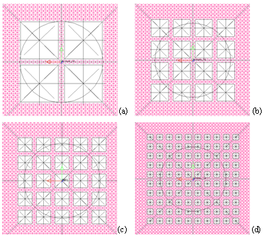
defined as the hollow arranged MAF.
Besides, the pixel spacing can be
designed as 53 μm, 126 μm or 179 μm,
which is corresponding to one, two or
three rows of microlenses in between the
sub-pixels. Figure 1 shows the
pixel-partition configuration of pixel
spacing by one row of microlenses, and
note that the black circle in each
configuration is the viewing aperture of
luminance meter for measurement and is
equal in size.
|
 |
|
Figure 1. Schematic
diagram of partitioned pixel units
attached hollow-arranged MAF. The unit
edge lengthes of sub-pixel are (a) 500
μm, (b) 250 μm, (c) 200 μm and (d) 100
μm. The spacing is one row of
microlenses and of 53 μm. |
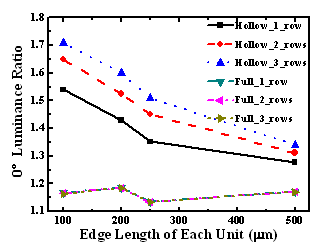
Hollow-arranged and
fully-filled MAF with one, two and three
rows of microlens in between the
sub-pixel spacing were modeled.
Considering normal direction luminance
ratio, fully-filled MAF shows from 13%
to 21% enhancement, which seems
irrelevant to the unit edge length of
sub-pixel. However, hollow-arranged MAF
presents as much as 67% improvement. As
the unit edge length of the sub-pixel
decreases, the luminance ratio of
hollow-arranged MAF will increase
linearly; as increment of microlens rows
inside the gap in between the
sub-pixels, the luminance ratio of
hollow-arranged MAF will also increase,
as shown in Figure 2.
|
 |
|
Figure 2. Luminance
ratio of hollow-arranged and
fully-filled MAF vs. edge length by
varying the sub-pixel spacing in the
unit of microlens rows. |
The Roles of Thermally Evaporated Cesium
Carbonate to Enhance the Electron
Injection in Organic Light Emitting
Devices
Professor Chih-I Wu
Graduate Institute of Photonics and
Optoelectronics, National Taiwan
University
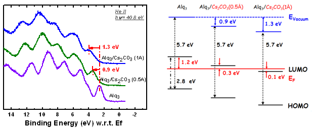
The
properties of thermally evaporated
cesium carbonate (Cs2CO3)
and its role as electron injection
layers in organic light emitting diodes
were investigated. According to the
ultraviolet photoemission spectra (UPS),
the Fermi level of Alq3 after
doped with Cs2CO3
shifts toward or into the lowest
unoccupied molecular orbital (LUMO) as a
result of chemical reaction and charge
transfer between Cs2CO3
and Alq3, which lowers the
electron injection barrier and improves
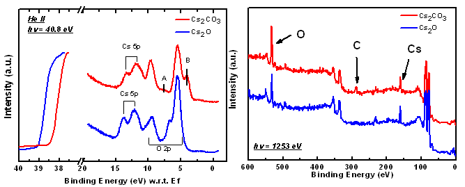
the current efficiency. As for whether
Cs2CO3 being
decomposed during the evaporation, we
found that Cs2CO3
molecules were deposited on the
substrates without decomposition,
regardless the evaporation rates, based
on the signature features of carbonate
groups and ionization energies measured
in UPS spectra and the binding energy
shifts of core level electrons. The
reaction mechanisms between Cs2CO3
and Alq3 are also proposed.
Since Cs2CO3 not
only being used in the electron
injection layer but also in converting
high work function materials to
cathodes, we further quantitatively
investigated the work function
modification of indium-tin-oxide (ITO)
with deposition of Cs2CO3
at the surfaces. We found that while 0.5
angstrom thick of Cs2CO3
is sufficient to reduce the electron
injection barrier of Alq3,
the thickness needed to convert ITO
surface to low work function cathode is
about 10 angstroms.
|
 |
|
(a) |
(b) |
|
Fig. 1 (a) UPS spectra of Alq3
near the valence bands with ultra-thin
layer of Cs2CO3
deposition. (b) Energy band diagram of
Alq3 with Cs2CO3
deposition. |
|
 |
|
(a) |
(b) |
|
Fig. 2 (a) UPS spectra of Cs2CO3
and Cs2O films on gold
samples, near the onset and valence
bands. Peaks A and B are the signature
features of carbonate. (b) XPS spectra
of pristine Cs2CO3
and Cs2O. |
|
|
|
|
|
|
| |
|
|
 |
|
 |
|
|
|