|
|
 |
|
 |
| |
Publisher:
Chairman Sheng-Lung Huang Editors:
Prof. Jui-che Tsai, Ms. Hsiao-wen Lin June 30,
2009 |
| |
|
 |
|
Congratulations!
GIPO Professor Ching-Fuh Lin receives
the title of “Member of Asia-Pacific
Academy of Materials”~
|
|
 |
|
 |
|
| |
|
|
|
February GIPO Lecture Highlights |
|
|
February 13th, 2009 (Friday),
10:30 am |
|
Speaker: |
Dr.
Lars Zimmermann (Technical
University of Berlin, Germany) |
|
Topic: |
Photonic integration in high-performance 0.13µm SiGe BiCMOS technology |
| |
Dr. Lars Zimmermann visited GIPO on
February 13th, 2009 (Friday), and
lectured in Room 103, Barry Lam
Hall. His lecture on “Photonic
integration in high-performance
0.13µm SiGe BiCMOS technology” was
attended with enthusiasm by GIPO
professors and students. Everyone
learned much. |
|
March
“Photonics Forum”
Lecture Highlights |
|
|
March
3rd, 2009 (Tuesday), 1:30 pm |
|
Speaker: |
Dr.
Young-Kai Chen (Bell Lab.,
Alcatel-Lucent Technology, U.S.A.) |
|
Topic: |
High
speed electronics and
optoelectronics for optic fiber
communications |
| |
Dr. Young-Kai Chen visited GIPO on
March 3rd, 2009 (Tuesday). He
lectured in Auditorium 101, Barry
Lam Hall on the topic of “High speed
electronics and optoelectronics for
optic fiber communications”. The
lecture was attended with enthusiasm
by GIPO professors and students, and
everyone learned much. |
|
 |
|
Dr. Young-Kai Chen
(middle) with GIPO Chairman Sheng-Lung
Huang (left) and GIEE Chairman Shey-Shi
Lu (right) |
|
|
|
April
“Photonics Forum”
Lecture Highlights |
|
|
|
April 10th,
2009 (Friday), 2:30 pm |
|
|
Speaker: |
Mr.
Wei-Ming Huang (AU Optronics Corp.,
AC Technology Div. Director) |
|
Topic: |
A
Summary of TFT-LCD Industry and
Technology |
| |
Mr. Wei-Ming Huang visited GIPO on
April 10th, 2009 (Friday). He
lectured in Room 113, Barry Lam Hall
on the topic of “A Summary of TFT-LCD
Industry and Technology”. GIPO
professors and students attended the
lecture with enthusiasm and learned
much. |
|
|
|
|
|
April 24th, 2009
(Friday), 2:30 pm |
|
|
Speaker: |
Professor Chi-Kuang Sun ( GIPO,
National Taiwan University) |
|
Topic: |
Optical Virtual Biopsy Based On
Least-Invasive Harmonic Generation
Microscopy |
| |
Professor Chi-Kuang Sun was
specially invited to speak in
Auditorium 101, Barry Lam Hall on
the topic of “Optical Virtual Biopsy
Based On Least-Invasive Harmonic
Generation Microscopy”. Professor
Sun has made outstanding and
innovative contributions in
photonics and optoelectronics
technology and received the title of
IEEE Fellow. His research team’s
groundbreaking achievements have not
only been published by several noted
journal, but have also been cited
numerous times by important
international academic media. His
lecture incited eager participation
from all GIPO professors and
students, and everyone learned much.
|
|
|
|
|
|
| |
|
|
~ The 3rd Seoul National University-National Taiwan University Student
Workshop 2008 on Photonic Materials and Devices ~
Time: December 14th ~
19th, 2008
Location: Seoul National University
Composed by
Min-Yung Ke, GIPO
Ph.D. candidate
(Team
Leader, representative student
team)
Near the end of October, I received a letter from my
professor, asking if I was interested in taking part in the 3rd National
Taiwan University-Seoul National University Student Workshop. I replied
“yes”, thinking that this would be an opportunity to do some travelling.
However, at the 1st NTU pre-seminar meeting, I was unexpectedly elected
the leader of the NTU team, responsible for planning and managing the
event.
My interaction with Seoul began when I sent out an e-mail
to the team leader of the Seoul group. After the initial greetings and
polite exchanges, I realized that I had already met their leader back
when we both took part in the 2nd Student Workshop. We exchanged MSN
accounts immediately and began our intensive discussions and planning,
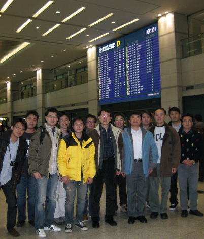
which lasted until our NTU team flew to Korea on December 14th.
Our team was groggy and tired when we first landed, since
we woke early to catch our flight. However, the cold air (0~ -2℃ ) in
Korea woke us instantly. After excitedly buying Korea’s famous "banana
milk", we waited for the SNU leader to come and pick us up from the
airport, admiring the beauty of Korean girls while we waited.
|
 |
|
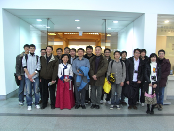
Students
and professors waiting at the airport |
After our arrival at SNU and a short break, the SNU team
leader and several students showed us around the campus. The campus is
located in a mountainous area in the suburbs of Seoul, an area often
frequented by hikers. Excluding the scattered high-rise buildings, the
campus looked more like an ideal place for mountain climbing and hiking
to us visitors from Taiwan. While touring and appreciating the campus
scenery, we chatted with the Korean students, about student life and the
rewards and challenges of our research.
|
 |
|
On the SNU campus |
After a good night's rest, the 3rd National Taiwan
University-Seoul National University Student Workshop began the next
morning. I listened to several reports on differing fields, delivered by
both NTU and SNU students. I then noticed that, regardless of the
outcomes of research, SNU students were better at expressing and putting
forth the strengths of their research. With this ability, they were able
to impress their listeners as they introduced their university.
Koreans are known to us, perhaps, as an
energetic people. After planning the workshop itinerary with the SNU leader and interacting with SNU students during the workshop, I’ve
also come to realize that they are not so different from people around us.
They were enthusiastic and hospitable during our visit; during private
discussions, they generously shared their research ideas with us. It
seems to me that their life plans and goals are much the same as mine.
In the last few days after the seminar, we visited some
ancient monuments and scenic areas in the suburbs of Seoul. We came to
realize that the old Korea had been heavily influenced by Chinese
culture. Nowadays their constant efforts and progress have made them a
country to be respected, and SNU has also become one of the top 100
universities in the world. Participants of this year’s workshop were all
doctoral students; they demonstrated positivity and self-confidence,
fully identifying themselves with their studies and their environment.
It seems to me that this positive attitude is less apparent in Taiwanese
students. I feel that we can build our strength by learning from their
attitude, and increase our ability to compete.
I would like to thank GIPO for providing us with this
opportunity to take part in the workshop. Generally, during
international conferences, we would merely deliver our reports and
listen to others' reports, not interacting much with other participants.
However, through this exchange, we interacted with SNU students and
gained an understanding of the differences in thinking and in attitudes
between students of different countries. Although I am back in Taiwan, I
believe I have gained a lot from this workshop.
Composed by Chun-Da Liao,
GIPO Ph.D. candidate
The 3rd National Taiwan University-Seoul National
University Student Workshop took place at SNU, Korea, on December 15th,
2008. The seminar was focused on the application of photonic materials
and components. Discussions covered five topics: optical
characterization and modeling, wide band-gap semiconductors, OLED,
infrared optoelectronics, and photonic devices. The four-day exchange
event also included visits to Korea Advanced Nano Fab Center (KANC),
Advanced Institute of Convergence Technology (AICT), and
Inter-university Semiconductor Research Center (ISRC). In addition,
tours exploring Korean culture and cities enhanced the exchange
resulting from this event. We were provided with the opportunity to meet
graduate students from other countries and to learn from each other,
broadening our vision and horizons.
Korean graduate students like to chat about topics such
as daily studying hours, interaction between advisors and students,
students' salaries, and ways to ease pressure, just as Taiwanese
graduate students do. Daily studying hours are about the same between
the students of both universities. However, in Korea, a country renowned
for its love of video games, students are unable to connect to any
gaming website during class hours, which is not the case in Taiwan.
Sports and music are common ways of alleviating pressure. Unlike Taiwan,
however, Korean graduate students, and even professors, like to gather
in small groups to drink a little and relax. In fact, there are bars on
campus. As to research facilities, I think there are some things we
could learn from SNU. Although NTU has plenty of research facilities and
equipment, they are scattered all over campus, making them inconvenient
to use. I believe that if we could build a large research center,
bringing together all those facilities, and establish a comprehensive
system of management, we would be more able to increase NTU's
competitiveness in the international engineering field. As we can see
from the development of industries of TFT-LCD, LED, OLED, and solar
cells, Korea and Taiwan are generally on the same track in the area of
photonics.
|
 |
 |
|
Participating professors and students at
the workshop |
Tour of the KANC |
In addition to what was mentioned above, city tours
allowed me to see more likeness between Korea and Taiwan. Some streets
in downtown Seoul look very much like those in Taipei. For example,
Seoul's Myeong-dong and Insa-dong look like Taipei's Ximen-ding and East
Area (“dong” and “ding” seem close in meaning). Korean students like to
visit these places during weekends and holidays as well. Seoul Tower,
built on a hill, overlooks Seoul and its beautiful night view, just as
Taipei 101 overlooks Taipei. The resemblance between Korean and
Taiwanese cultures is even more apparent when visiting the art gallery
and Changdeokgung Palace. With regard to writing and language, Chinese
characters can be seen in many places in Korea, and some Taiwanese
pronunciation is similar to Korean pronunciation. In terms of geography,
both Taiwan and Korea are close to China. Therefore, it is easy to see
the many resemblances between the two countries.
From this event, we have been inspired and learned a lot
in terms of research and in terms of culture. I would like to thank the
graduate students of SNU for their generous hospitality; Chairman Huang,
Vice Chairman Lin and Professor Su for sharing their experiences during
this trip.
|
 |
 |
|
Tour of the KANC |
At the Seoul Museum of History |
|
|
|
|
|
|
|
| |
|
|
|
Characteristic Investigation of 2D Photonic Crystals with Full Material Anisotropy under Out-of-Plane Propagation and Liquid-Crystal-Filled Photonic-Band-Gap-Fiber Applications Using Finite Element Methods
Professor Hung-chun Chang
Graduate Institute of Photonics and Optoelectronics,
National Taiwan University
To effectively investigate the fundamental
characteristics of two-dimensional (2D)
photonic crystals (PCs) with arbitrary
3D material anisotropy under the
out-of-plane wave propagation, we
establish a full-vectorial finite
element method based eigenvalue
algorithm to perform related analysis
correctly. The band edge diagrams can be
conveniently constructed from the band
structures of varied propagation
constants obtained from the algorithm,
which is helpful for the analysis and
design of photonic band gap (PBG)
fibers. Several PCs are analyzed to
demonstrate the correctness of this
numerical model. And the validity of
those for the most complex PC with
arbitrary 3D anisotropy is supported by
related liquid-crystal-filled PBG fiber
mode analysis, which demonstrates the
dependence of transmission properties on
the PBGs, employing a full-vectorial
finite element beam propagation method
(FE-BPM). (Optics Express, vol. 16, no.
26, pp. 21355–21368, 22 December 2008.)
|
 |
|
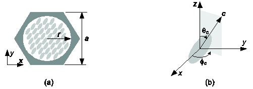
Fig. 1. (a) The unit cell of a 2D PC with triangle-arranged liquid-crystal-filled holes in the silica. (b) Schematic definition of rotation angles for the liquid-crystal (LC) molecule. |
|
 |
|
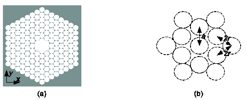
Fig. 2. (a) The cross-section of an LC-core PCF. The PCF is assumed to be made of chalcogenide glass with the cladding region formed by triangle-arranged LC-filled holes. (b) The schematic geometry of the core region for (a), which is also filled with LCs. |
|
 |
|
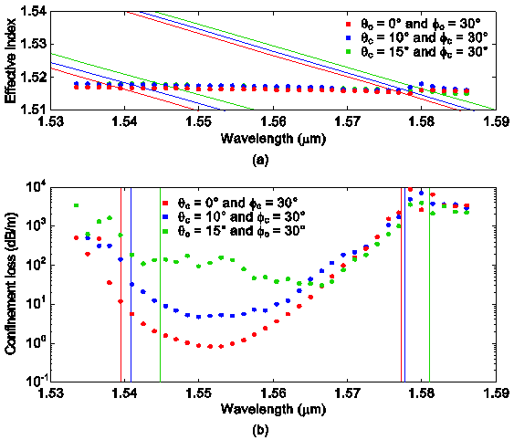
Fig.
3. (a) The effective index and (b) the confinement loss of the
y-polarized fundamental mode for the LC-core PCF of
a = 2.26
μm with six rings of LC-filled holes, as shown in Fig. 2, obtained using the FE-BPM. The solid lines denote the PBG boundaries derived from the calculated band edge diagrams. Different colors are used to distinguish the results for different orientations of the LC molecules. |
Enhanced and partially polarized output of a light-emitting diode with its InGaN/GaN quantum well coupled with surface plasmons on a metal grating
Professor C. C. Yang
and Professor Yean-Woei Kiang
Graduate Institute of Photonics and
Optoelectronics, National Taiwan
University
The enhanced and
partially polarized output of a green
light-emitting diode (LED), in which its
InGaN/GaN quantum well (QW) couples with
surface plasmons (SPs) on a surface Ag
grating structure is demonstrated.
Compared with an LED sample of no (flat)
Ag coating, the total output intensity
of an LED of SP-QW coupling can be
enhanced by ~59 (~200) % when the
grating period and groove depth are 500
nm and 30 nm, respectively. Also, a
bottom-emission polarization ratio of
1.7 can be obtained under the condition
of 15 nm in groove depth.
|
 |
|
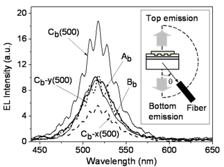
Fig. 1 LED
bottom-emission spectra of samples
A,B,and C(500).The subscript b in a
sample notation represents bottom
emission.In the insert, the setup for
angle-dependent LED output intensity
measurement is schematically shown. |
|
 |
|
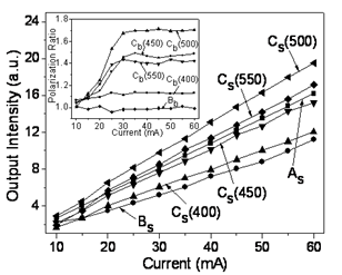
Fig. 2 Total LED
output intensities as functions of
injection current of samples A, B, and C
series. In the insert, the polarization
ratios of bottom emission in various
samples as functions of injection
current are demonstrated. The subscript
s in a sample notation represents total
intensity. |
|
 |
|
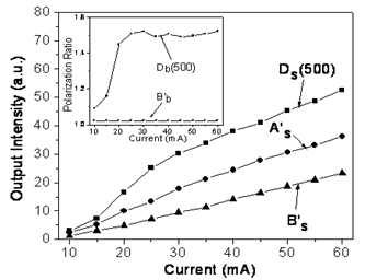
Fig. 3 Total LED output intensities as functions of injection current of samples A’, B’, and D(500). In the insert, the polarization ratios of bottom emission in samples B’ and D(500) as functions of injection current are demonstrated. |
|
 |
|
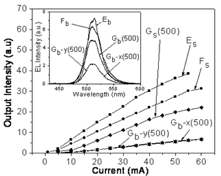
Fig. 4 Total LED output intensities as functions of injection current of samples E, F, and G(500), including its two polarization components of bottom emission. The spectra of the corresponding LED outputs of bottom emission at 40 mA are shown in the insert.
|
Study on the decay mechanisms of surface
plasmon coupling features with a light emitter
through time-resolved simulations
Professor Yean-Woei Kiang
and Professor C. C. Yang
Graduate Institute of
Photonics and Optoelectronics, National
Taiwan University
The transient behaviors of the dipole
coupling with surface plasmon (SP)
features in an Ag/dielectric-interface
grating structure in order to understand
the characteristics of those
dipole-coupling features are
demonstrated. In particular, the major
decay mechanisms of those coupling
features can be identified. For
comparison, the time-resolved behaviors
of the resonant surface plasmon
polariton (SPP) coupling feature on a
flat interface are also illustrated.
Among the three major grating-induced
SP-dipole coupling features, two of them
are identified to be localized surface
plasmons (LSPs). The third one is a
grating-assisted SPP, which shows two
decay components, corresponding to the
first stage of SPP in-plane propagation
and the second stage of coupling system
decay. In all the dipole coupling
features, metal dissipation can dominate
the energy relaxation process, depending
on the assumption of damping factor. All
the dissipation rates are proportional
to the assumed damping factor in the
Drude model of the metal. The
dissipation rates of the LSP and
resonant SPP features are about the same
as the damping rate, implying their
local electron oscillation natures. The
dissipation rate of the grating-assisted
SPP feature is consistent with
theoretical calculation. In the LSP
features under study, dielectric-side
emission is prominent. The coupled
energy in the grating-assisted SPP
feature can be efficiently stored in the
coupling system due to its low emission
efficiency and effective energy
confinement through grating diffraction.
|
 |
|
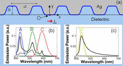
Fig. 1. (a) Two-dimensional
Ag/dielectric grating structure in the
x-y plane. The dipole, Jx, is located 10
nm right below the center of a grating
groove, which is defined as the origin,
O, of the coordinate system. The flat
interface structure is depicted by the
dotted line along the x axis. (b) The
dipole radiation power spectrum
(continuous curve), the dielectric-side
emission spectrum of the SP-dipole
coupling system (dashed curve), the
radiation power spectrum of the control
case (dotted line near the bottom), and
three source spectra (dashed
Gaussian-like curves) for the three
SP-dipole coupling features (A-C) in the
grating structure. (c) The dipole
radiation power spectrum (continuous
curve), the dielectric-side emission
spectrum of the SP-dipole coupling
system (dashed curve), and the source
spectrum (dashed Gaussian-like curve)
for the SP-dipole coupling feature D in
the flat-interface structure. |
|
 |
 |
|
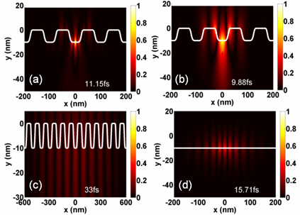
Fig. 2. Field strength (absolute
value of Hz) distributions of the
dipole-coupling features A-D in
parts (a)-(d), respectively, at the
individually chosen delay times for
showing the broadest field
distributions along the x axis when
g
=
g0.
|
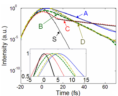
Fig. 3. Time-resolved field
intensity profiles at point O of the
four SP-dipole coupling features.
The source profile is shown and
labeled by S. The fitting lines for
calibrating the decay times are
plotted. The insert shows the
linear-scale profiles for
demonstrating the temporal peak
positions. The damping factor
g
is set at
g0. |
Research Accomplishments in 2008, Wide
Gap Semiconductor Laboratory
Professor Zhe-Chuan
Feng
Graduate Institute of Photonics and
Optoelectronics, National Taiwan
University
l “Structural and Optical Studies on
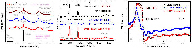
Ion-implanted 6H-SiC Thin Films”, Z.C.
Feng, et al., Thin Solid Films,
516,
5217-5226 (2008).
Below are Raman and IR spectra for
C+/Al+ co-implanted & annealed 6H-SiC
l
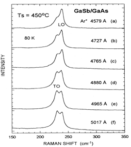
“Optical Investigation of GaSb Thin
Films Grown on GaAs by Metalorganic
Magnetron Sputtering”, Z.C. Feng,
et al.,
Thin Solid Films,
516,
5493-5497 (2008).
|
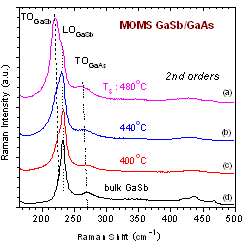 |
←
Raman spectra from three MOMS-grown
GaSb/GaAs (001) grown at substrate
temperature of (a) 480℃,
(b) 440℃
and (c) 400℃,
and (d) a bulk GaSb.
←
→
Raman spectra from a MOMS-grown GaSb
on GaAs (100) with Ts =
480℃,
under different
excitation wavelengths between 4579
and 5017 Å from an Ar+ laser.
→
|
 |
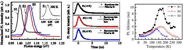
l
“Emission dynamics of InAs
self-assembled quantum dots with
different cap layer structures”, L.M.
Kong, Z.C. Feng, et al.,
Semiconductor Sci.
& Technol.,
23,
075044-8 (2008).
Below are PL, TRPL and decay time-T plots of three InAs-QDs with
different cap layer structures.
|
l
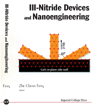
Book
<III-NITRIDE DEVICES AND
NANOENGINEERING>,
Zhe Chuan Feng (National
Taiwan University),
Imperia College Press, London, 462
p., 2008.
http://www.icpress.co.uk/cgi-bin/htsearch,
ISBN 978-1- 84816-223-5.
This book, consisting of 15-well
written review chapters, provides
useful information to the device and nano-scale process, fabrication of
LEDs, LDs, photodetectors and nano-devices,
characterization, application and
development
on the III-Nitrides semiconductor
devices and nano-engineering.
l book
chapter,
“Structural and optical properties
of InGaN/GaN multiple quantum well
light emitting diodes grown by
metalorganic chemical vapor
deposition”,
Z.C. Feng
et al., in
<<III-Nitride Devices and Nanoengineering>>, Chapter 3,
pp.57-88, Imperial College Press,
London, UK (2008).
|
 |
|
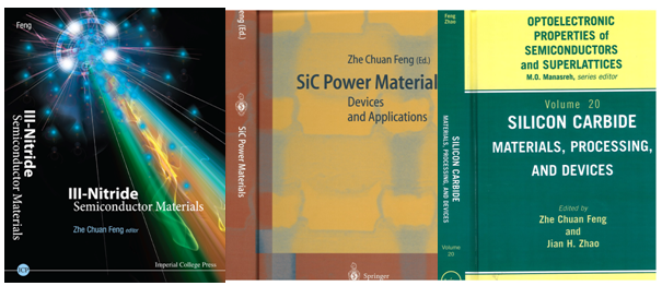
In additions, Prof. Feng has in
recent years published a series of
specialized review books from world
famous scientific publishers in USA,
Germany, UK and Singapore,
especially for wide gap
semiconductors:
<III-NITRIDE SEMICONDUCTOR
MATERIALS>,
Zhe Chuan Feng
(National Taiwan University),
Imperia College Press, London, 440
p., 2006.
ISBN 978-1-86094-636-3,
(12-chapters)http://www.icpress.co.uk/cgi-bin/htsearch.
<SiC Power Materials Devices and
Applications> by Zhe Chuan Feng (National
Taiwan University), 450 p., 2004.
ISBN: 978-3-540-20666-8,
http://www.springer.com/materials/.
(11-chapters)
<Silicon Carbide: Materials,
Processing and Devices> by Zhe Chuan FENG/Jian H. ZHAO, Taylor &
Francis Books, New York, 416 p.,
2003. ISBN: 9781591690238,
http://www.taylorandfrancis.co.uk/.
(8-chapters)
<POROUS SILICON>, Z C Feng & R Tsu,
World Scientific Publishing,
Singapore, 488 pages.
<Semiconductor Interfaces,
Microstructures and Devices:
Properties and Application>, Zhe
Chuan FENG, Institute of Physics
Publishing, Bristol, 308 pages.
<Semiconductor Interfaces and
Microstructures>, Zhe Chuan FENG,
World Scientific Publishing,
Singapore, 328 pages,
http://www.worldscibooks.com/nanosci/1568.html
|
 |
Organic-Inorganic Composite Thin-Film
Solar Cells
Professor Ching-Fuh
Lin
Graduate Institute of Photonics and
Optoelectronics, National Taiwan
University
Solar
cells attract great attention recently
owing to the growing need for renewable
energy. In particular, polymer solar
cells offer the potential of large-scale
power generation based on materials that
provide flexibility, light weight,
low-cost production and low-temperature
fabrication. The most common and
efficient material system so far for
polymer devices is the one consisting of
poly(3-hexylthiophene) (P3HT) and
(6,6)-phenyl C61 butyric acid methyl
ester (PCBM). However, the conventional
bulk-heterojunction (BHJ) architecture
has limitations in device stability.
Exposure of the conventional solar cells
to air leads to oxidation of the Al
electrode and degradation of the indium
tin oxide (ITO)/poly(3,4-ethylene
dioxythio- phene): poly(styrene
sulfonate) (PEDOT: PSS) interface
because of the acidic nature of
PEDOT:PSS.
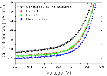
To overcome the above difficulties,
inverted configuration with
semiconductor oxides is investigated in
our Lab. The inverted structure has the
advantage of improved stability by
replacing both the low work function
metal cathode and PEDOT:PSS. In
addition, the environ- mentally friendly
and low-cost ZnO is particularly well
suited for this application as they can
be deposited at low temperature. ZnO
also provides hole blocking function.
Furthermore, we develop low-temperature
solution processes of transitional metal
oxides deposited on top of the active
layer to serve as the electron blocking
layer. With the active layer sandwiched
between the ZnO and the transitional
metal oxide layers, the devices have the
electrons and holes forced to transport
separately toward opposite electrodes
for efficient carrier collection, so
greatly improving the power conversion
efficiency (PCE) of solar cells.
Using P3HT/PCBM in the active layer, the
inverted structure of polymer solar
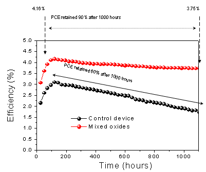
cells gives the PCE of 4.16 % (Fig. 1).
The lifetime test shows that the PCE
still retains 90% of the maximum value
after 1000 hours of operation (Fig. 2).
As the device is fabricated on the
flexible polyester (PET) substrate, the
PCE can also be 3.66%, the highest among
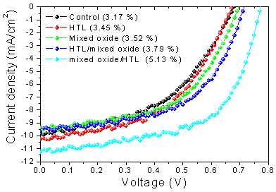
the solar cells on flexible substrates.
If the PV2000 is used for the active
layer, the PCE is even as large as 5.13
% (Fig. 3), which is the highest among
the solar cells with inverted
structures.
|
 |
|
Fig. 1 J-V curves of polymer solar cells using P3HT/PCBM. |
|
 |
|
Fig. 2 Reliability test of polymer solar cells using P3HT/PCBM. |
|
 |
|
Fig. 3 J-V curves of polymer solar cells using PV2000. |
Narrow-Band Metal-Oxide-Semiconductor UV
Photodetector
Professor Chee-Wee Liu
Graduate Institute of Photonics and
Optoelectronics, National Taiwan
University
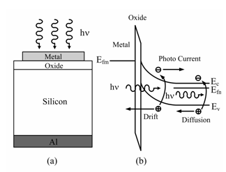
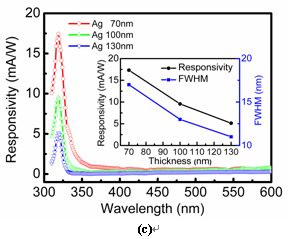
Si-based photodetector for narrow-band ultraviolet light (319nm) detection is demonstrated using a metal-oxide-semiconductor tunneling structure. By using appropriate selection of gate metal, the metal-oxide-semiconductor tunneling diode can detect the UV light. Due to the spectral dependence of absorption and reflection of the Ag as gate electrode, the narrow-band detection of ultra violet can be achieved. The photodetectors with 130nm thick Ag gate exhibit peak responsivities of 5.1mA/W at 319nm.
|
  |
|
Fig. 1: (a) A Schematic structure of Metal-Oxide-Semiconductor tunneling photodetector. (b) Mechanism of the photocurrent formation. (c) Spectral responses of the MOS tunneling photodetector with the 70nm, 100nm, and 130nm Ag electrode. The inset shows the FWHM and the peak responsivity versus metal thickness.
|
The schematic structure
of the MOS tunneling photodetector is shown in Fig. 1 (a). When the photons selected by the metal gate with energy larger than the bandgap of Si (1.12eV) illuminate on the gate electrode, the photo-generated electron-hole pairs in the depletion region can be separated by the built-in electric field in the depletion region (Fig.1 (b)). The photo-generated holes in the diffusion length away from the depletion edge can also reach the depletion region by diffusion. For the Ag thickness of 70nm, 100nm, and 130nm, the peaks of the spectral responses are located at 319nm with value of 17.3mA/W, 9.6mA/W, and 5.1mA/W, respectively (Fig. 1 (c)). The thickness of Ag can modulate the spectral response of photodetector. For thick Ag, the full width at half magnitude (FWHM) decreases but the responsivity also drops (the inset of Fig. 1 (c)).
In summary, the wavelength selection of metal-oxide-semiconductor detector is demonstrated by gate electrode. The gate electrode is not only used for reading out the electronic signal but also used as a filter to select the narrow band photons to enter the Si for further absorption. Due to the spectral dependence of absorption and reflection of the Ag as gate electrode, the UVB detector is demonstrated by Ag.
|
|
|
|
|
|
| |
|
|
 |
|
 |
|
|
|