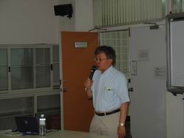
![]() Vice Chairman Sheng-Lung Huang
engaged as the Topic Editor of the world-
Vice Chairman Sheng-Lung Huang
engaged as the Topic Editor of the world-
renowned journal Optics Letters.
|
In August of 2005, Vice Chairman Huang began his three-year term as the Topic Editor of Optical Society of America’s (OSA) Optics Letters, overseeing the management of submissions within the category of optical measurement, components, and devices. In 2004, Optics Letters achieved an Impact Factor of 3.882, the highest among the 40 journals of JCR’s Optics category that widely accept submissions of contributed papers; the journal is also listed as one of the outstanding journals of the College of EECS. Optics Letters limits its acceptance rate to 50%. Vice Chairman Huang is quite possibly the first person in Taiwan to join the editorship of a journal with such a high Impact Factor. |
|
![]() Professor Sheng-Lung Huang is reappointed as the Vice
Chairman of GIEOE~
Professor Sheng-Lung Huang is reappointed as the Vice
Chairman of GIEOE~
Professor Sheng-Lung Huang has fulfilled the role of Vice Chairman of GIEOE for half a year and provided exemplary performance. With the Dean’s approval, Professor Huang has been reappointed as the Vice Chairman for another year.
![]() Spotlight of New Faculty Member: Prof. Gong-Ru
Lin
Spotlight of New Faculty Member: Prof. Gong-Ru
Lin
Curriculam Vitae and Professionalism of Prof. Gong-Ru Lin
|
Faculty Posistion |
Name |
Education |
Fields of Professionalism |
Working Experiences |
|
Professor |
Gong-Ru Lin |
Ph. D. in Electro-Optical Engineering |
Si Nanophotonics for Light Emission and Solar Energy Transfer, Femtosecond Fiber Lasers and Applications, High-speed All-optical Fiber Communication Data Processing |
1. National Chiao Tung University, Institute of Electro-Optical
Engineering,
Professor, 2004/08-2006/07
Engineering,
Associate Professor, 2002/08-2004/07
Technology, Associate Professor,
2001/08-2001/07
Professor, 2001/02-2001/07
Professor, 1998/08-2001/01
Optical
Engineering, assistant Professor,
1997/08-1998/07
Engineering, Post Doctoral Fellow,
1997/01-1997/07 |
![]() Dr. Y. K. Chen Visits~
(July 7, 2006)
Dr. Y. K. Chen Visits~
(July 7, 2006)
|
Dr. Y. K. Chen, an eminent scientist in optical fiber communications, visited GIEOE on July 7 of 2006 and gave a lecture on “Recent Advances in Optical Signal Generation and Processing for Optic Fiber Network.” Dr. Y. K. Chen currently holds a post at Bell Labs, Lucent Technologies and has received the IEEE David Sarnoff Award. He is a Fellow of IEEE and also a Member of the U.S. National Academy of Engineering. This year, Dr. Y. K. Chen was nominated for the Fellow of the Academia Sinica. |
|
![]() Professor Pak-Lim Chu Visits~
(July 7, 2006)
Professor Pak-Lim Chu Visits~
(July 7, 2006)
|
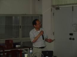
Professor Pak-Lim Chu, a prominent scientist in optical fiber communications, visited GIEOE on July 7 of 2006 and delivered a lecture on “Writing Gratings in Polymer Optical Fibre.” Professor Pak-Lim Chu received his Ph.D at University of New South Wales, Sydney, Australia, and is currently a Chair Professor of the Department of Electronics Engineering and the Director of the Optoelectronics Research Centre at the City University of Hong Kong. Professor Chu has been awarded the Australian Centenary Medal for contributions in optical communications by the Australian government. |
|
![]() Professor Pochi Yeh Visits~
(July 14, 2006)
Professor Pochi Yeh Visits~
(July 14, 2006)
|
Professor Pochi Yeh, an eminent scientist in photonics, visited GIEOE on July 14 of 2006 and delivered a lecture on “Birefringent Thin Films for LCDs.” Professor Pochi Yeh is currently a Professor of the Department of Electrical and Computer Engineering at University of California, Santa Barbara. His work has focused on phase conjugation, optical computing, and LCD. Professor Yeh holds authorship of many widely-read optoelectronics books and is Fellow of both IEEE and OSA. |
|
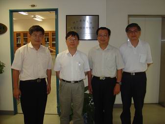
![]() Professor Simon Fleming Visits~
(July 10, 2006)
Professor Simon Fleming Visits~
(July 10, 2006)
|
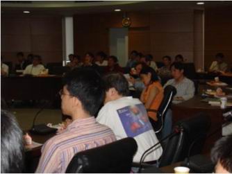
Prof. Simon Fleming, Director of the Optical Fibre Technology Centre (OFTC), The University of Sydney, was invited to make a short visit to our Institute on July 10. He attended the OECC 2006 conference in Kaohsiung in early July and was able to stay in Taipei for a few days before returning to |
|
|
|
Australia. He met several colleagues having research activities related to optical fiber communication technologies in the lunch hosted by Chairman Yang. Then, after a brief visit of EE Building II, he was able to get some idea of the organization and research activities of our Institute and the College of EECS. The OFTC was established in 1988 to undertake research and development in the design, fabrication, and applications of special fibers. In 2004, the OFTC established a microstructured polymer optical fiber (mPOF) facility and the activities in the R & D of polymer photonic crystal fibers have been internationally well known. Prof. Fleming joined the OFTC in 1994 and his current research is focused on technologies of poled fiber devices. |
|
Photo of Prof. Fleming (fourth from the left) taken with professors of the Institute |
|
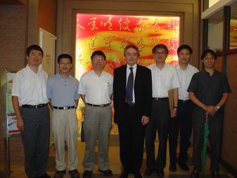
![]() Professor Anshi Xu Visits~
(July 25, 2006)
Professor Anshi Xu Visits~
(July 25, 2006)
|
Prof. Anshi Xu, Chairman of Department of Electronics, Peking University, visited our Institute on July 25, accompanied by Prof. Shien-Kuei Liaw of the National Taiwan University of Science and Technology. Prof. Xu also serves as the Director of the National Laboratory on Local Fiber-Optic Communication Networks & Advanced Optical Communication Systems (Beijing Section) and the Director of the Photonics & Communication Technology Institute of Peking University. His research areas include WDM automatic optical communication networks, high-speed large-capacity WDM fiber-optic communication systems, optical internet networks, coherent optical communication, and photonic devices. He was invited as a visiting |
|
 |
scholar to stay in the Department of Electronic Engineering of NTUST during the whole July. We were glad to have the opportunity to invite him to our campus and meet our faculty members. After viewing the research posters of the photonics laboratories in EE Building II, Prof. Xu commented that the research in our Institute was more focused on photonic devices. In Peking University, similar works have been mainly conducted in the physics related departments and institutes. He met and had joyful discussions with several colleagues having research activities related to fiber-optic communication technologies in the lunch hosted by Chairman Yang. It is expected that more academic exchanges between our Institute and Prof. Xu’s Department can be arranged in the near future. |
|
Photo of Prof. Anshi Xu (second from the right) taken with Prof. Shien-Kuei Liaw (first from the left), Chairman C. C. Yang (second from the left) and Prof. Hung-Chun Chang |
|
![]() Workshop on Nitride Compounds and their
Applications
Workshop on Nitride Compounds and their
Applications
![]()
May 12~13, 2006
Barry Lam Hall, National Taiwan University
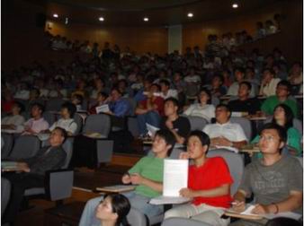
The Workshop on Nitride Compounds and their Applications, organized by the Graduate Institute of Electro-Optical Engineering, National Taiwan University and National Science and Technology Program for Nanoscience and Nanotechnology Program Office, was held in the Barry Lam Hall, National Taiwan University on May 12th and 13th 2006. Totally, 15 international and domestic scholars were invited to present their research accomplishments, including professors Ian Ferguson (Georgia Institute of Technology, US), Yasuhiko Arakawa (Tokyo University, Japan), Li-Chyong Chen, Shangjr Gwo, Yan-Kuin Su, Jen-Inn Chyi, Dong-Sing Wuu, Lung-Han Peng, Li-Wei Tu, Shing-Chung Wang, Ching-Ting Lee, Jenq-Dar Tsay, C. C. Yang, and W. N. Wang (Bath University, UK).
In the two-day workshop, there were totally 317 participants. They came from universities, industries, high schools, and research institutes. At the end of the workshop, Dr. W. N. Wang from Bath University was invited to share his experiences of representing UK and EU to visit the LED-related companies and research institutes in the United States and Japan. With the workshop, all the participants would have better understandings of the current development of the white-light emitting-diode technology.
 |
 |
![]() College of Electrical Engineering and Computer Science, National Taiwan
University
College of Electrical Engineering and Computer Science, National Taiwan
University
Commencement of Academic Year 2005–Highlights
![]()
June 3, 2006
Barry Lam Hall Square, National Taiwan University
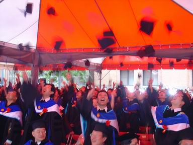 |
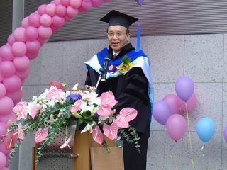
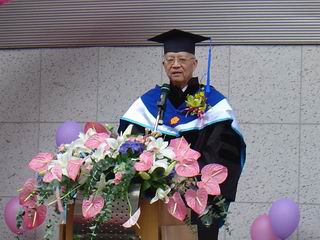
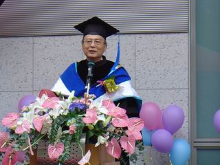
This year, the commencement of National Taiwan University took place on the morning of June 3. In the College of EECS, the “academic group” of Electrical Engineering, including Department of Electrical Engineering, Graduate Institute of Electro-Optical Engineering, Graduate Institute of Communication Engineering, and Graduate Institute of Electronics Engineering, also held a graduation ceremony on the same day, beginning at three o’clock in the afternoon at Barry Lam Hall square. President Si-Chen Lee was specially invited to deliver the opening remarks. President Chao-Han Liu of the University System of Taiwan was also invited to address the graduates, offering advice and good-wishes. Dean of the College of EECS, Soo-Chang Pei and graduate institute chairmen also provided remarks, encouraging the graduates to advance bravely and pursue their dreams after leaving NTU.
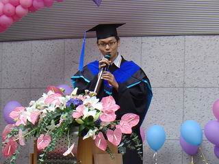
Next, after Kung-An Lin of GIEOE delivered a speech expressing the gratitude of all the graduates, the ceremony’s main event— conferral of diplomas and righting of the tassels commenced. As the students ascended the stage, accepted their diplomas, and took photographs with their advisors, the families and friends looking on from below stage, holding cameras and bouquets, must have felt happiness and extreme pride.
After the rituals of giving thanks to professors, then tossing caps, and cheering, the commencement neared its end. In the flowing music provided by the orchestra, the atmosphere of commencement was pervaded not only by a sense of nostalgia for the just-ended student career, but also by an exciting anticipation for the beginning of a new life.
 |
 |
| President Si-Chen Lee | President Chao-Han Liu of the University System of Taiwan |
 |
 |
| Dean of the College of EECS, Soo-Chang Pei | Kung-An Lin of GIEOE |
![]() OECC 2006 Report
OECC 2006 Report
![]()
July 3~7, 2006
Splendor Kaohsiung Hotel, Kaohsiung
OECC 2006 was held at the Splendor Kaohsiung Hotel from July 3 to July 7 in Kaohsiung. Last year, it was in Seoul, Korea, and will be held in Yokohama, Japan next year. This is the first time that Taiwan hosted OECC, which attracted scholars from 15 countries with near 450 paper submissions. About 65% of the submissions were from overseas.
Three plenary speeches were arranged. The first by Dr. Takashi Nakashima, NTT, Japan, on "FTTH Expansion in Japan." He presented the latest penetration of FTTH in Japan where the number of FTTH customers had already overtook that of CATV customers. The second by Dr. Victor Klimov, Los Alamos National Lab., U.S.A. He introduced how nanocrystals can dramatically enhance the spectral tunability and photoluminescence quantum yields, which make nanocrystals attractive for use in a variety of light-emitting technologies. Dr. Yung S. Liu, the former director of Opto-Electronics and Systems Labs. of ITRI delivered the third plenary speech. He emphasized that nanotechnologies have made light sources viable commercial products that impact immensely to our life, such as optical fiber communication, lasers, CD/DVD, etc.
Our faculty and students actively participated the conference in organizing, and in reviewing and submitting papers (See http://www.oecc2006.org for details). Professors C. C. Yang and Sheng-Lung Huang were co-chairs of the Technical Program Committee. Professor Hung-Chun Chang co-chaired the category of Optical Fibers, Fiber Devices, and Optical Sensing. Professors Hao-Hsiung Lin and Keanpgo Ricky Ho were committee members. The conference also invited Professor C. C. Yang and Chung-Chih Wu to deliver invited talks. Among the 12 student paper awards, 4 of them are from domestic works including 2 from our Institute by Mr. Sen-Ming Hsu and Min-Yann Hsieh.
OECC 2006 is the second large-scale international optoelectronics conference held in Taiwan (The first is the 5th Pacific Rim Conference on Lasers and Electro-Optics organized by Professor C. C. Yang in 2003), a summary will be posted in the November issue of IEEE Communications Magazine.
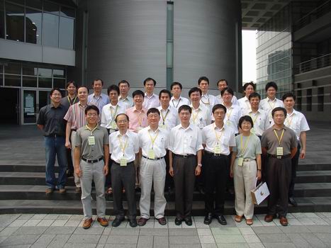
![]() NTU–Chi
Mei Research Collaboration Midterm Meeting
NTU–Chi
Mei Research Collaboration Midterm Meeting
![]()
July 20, 2006
Barry Lam Hall, National Taiwan University
|
|
|
Visitors from Chi Mei Group and NTU’s participating professors photographed in front of NTU Barry Lam Hall. |
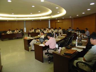
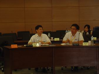
The Project, “Research Collaboration between National Taiwan University and Chi Mei Optoelectronics,” with Chairman C.C. Yang serving as the Principal Investigator, held its midterm meeting on July 20 in room 201 of Barry Lam Hall. On the meeting day, Chi Mei Optoelectronics Corporation’s (part of Chi Mei Group) technological development Deputy Head Director Dr. Chung-Kuang Wei led thirteen participants to visit and discuss the project. During the meeting, already-involved professors and junior professors reported on relevant research, eliciting enthusiastic discussions. Further advancement of the collaboration between both parties is eagerly anticipated. The following professors participated in the conference: Chairman C. C. Yang of the GIEOE; Yun-Shiuan Liao of the Department of Mechanical Engineering; Wei-Fang Su of the Institute of Polymer Science and Engineering; Feng-Yu Tsai, Miin-Jang Chen of the Department of Materials Science and Engineering; Tzong-Lin Wu of the GICE, Hoang-Yan Lin, Chih-I Wu, Jiun-Haw Lee, Jian-Jang Huang, Ding-Wei Huang, Guo-Dung Su, Yun-Li Li, Jui-Che Tsai of the GIEOE. Photographs of the meeting are as follows:
 |
 |
|
The meeting in progress |
Deputy Head Director Chung-Kuang Wei (left) and Director Kun-Feng Huang (right) of Chi Mei Optoelectronics Corporation |
|
|
|
|
I have been asked to give a summary of my time and experiences while living in Taiwan and teaching as a visiting professor at the Graduate Institute of Electro-optical Engineering (GIEOE) at National Taiwan University. I am writing this article about a week after leaving Taiwan so it has given me some time for reflection. My time in Taiwan can be simply summarized, as the title of the article suggests, that I was born Chinese in Taiwan and I now claim Taipei as my hometown. |
|

|
“At fifteen, I had my mind bent on learning.” National Taiwan University (NTU) is an excellent school with little or no difference from other leading Universities that I either worked in or interacted with in the last 20 years in both Europe and the U.S. It is clear that the caliber of its faculty and students rank with the best in the world. This can be best communicated to others by visitors, similar to me, who have an opportunity to interact with both the faculty and the students over an extended period of time. NTU also has a beautiful campus and I still have memories of walking around NTU seeing the petals from the azalea bushes arranged into Chinese characters on the ground during the spring. “By nature man are similar to one another, but learning and practice make them different.” There appeared to be little difference between the quality of the students I worked with in NTU and those I currently teach at the Georgia Institute of Technology (GaTech). The students in NTU were excellent and, if anything, were easier to work with as they were slightly more independent in both thought and action. As a consequence the students tended to ask fewer questions in the class than I would see at GaTech but would always find me independently if they needed help. All the students who attended the class that I taught should be commended since they had to learn a new topic and concepts in a non-native language. This is something that very few students could do elsewhere. I would hire many of the students that I worked with at NTU when they graduate if they had a desire to come to the U.S. |
||
|
“He who learns without thinking will be bewildered; he who thinks without learning will be in danger.” |
||
|
I have been asked if there are any suggestions that I can make to GIEOE, its faculty, and its students. This is a difficult question to answer since it is not easy to improve on excellence and many of my observations would not be valid due to a partial knowledge of language and culture. I can make some general comments because the educational system in Taiwan appears to have similar strengths and weaknesses as that in the U.S. For example, there is a focus on grades rather than the educational process. I often tell students that a ‘C’ is a good grade. It is better to learn that they are not competitive in an area during this one course during one semester rather than making a career choice in that area. However, many students miss the warning signs and this is often driven by family expectations to continue to work in that area. |
|
|
|
I like to use Blooms Taxonomy (see table) as the philosophical base for pedagogy. I often teach this in class, as I did at NTU, as students have typically not thought about how they learn or its philosophical consequences. The lower levels of Blooms Taxonomy (knowledge, comprehension and application) help us learn to replicate what has already been done elsewhere while the higher levels of Blooms Taxonomy (analysis, synthesis and evaluation) drive innovation. The current educational system appears to focus only on equipping the lower levels of functionality by using bounded problems with simple answers that can be quickly answered in homework or exams and are easy to grade. The higher levels of functionality require experience in solving unbounded problems with incomplete and/or complicated data sets which is typically more difficult to grade. Consequently, we often do our students disservice by not giving them an opportunity to solve these type of unbounded problems, which are more often seen. This leaves them ill equipped when they leave our institutions. |
||
|
"At thirty, I stood firm.” What impressed me most while staying in Taiwan was the generosity of the Taiwanese people. This not only included the people that I had the privilege to work with and to meet with on a regular basis. But, I also saw this generosity when I was visiting other schools, companies, and institutions around Taiwan and also the people we met on the streets. The character of the Taiwanese mirrored that of the Scots so I came to the conclusion that it must have to do with the morphology of the land; an island with ocean on one side, sea on the other, and mountains in between. Consequently, while in Taiwan I became Chinese and obtained a Chinese identity through a name, 傅 奕 曦 (see insert). I would tell people that I was Chinese, but only 3-4 months old at this time, but they do not believe me. So, then I tell them that I am ‘Scottish born Chinese’ (SBC), and this meant that my facial features were different to other Chinese, that I did not speak the language and neither of my parents were Chinese. And, since they have not met many SBC’s, this left them confused. |
|
||
|
“At forty, I had no doubts.” A search on amazon.com shows that there are many books covering the theme, ‘Lost in Translation’, essentially an investigation of someone adapting to a foreign culture. This theme was more recently explored in a movie of the same name that won an Oscar for the director, Sofia Coppola. In returning home I have experienced a different, but related phenomena, which I have named ‘Lost in Transition’; the things that were common place to you in the new culture that are now missing. These include struggling to find some Chinese words to show your gratitude to someone, and trying to understand and/or recognize new Chinese characters. Other points of transition are complicated to understand; such as, when in Atlanta, seeing a non-Chinese person walking down the street by themselves and thinking of them as a foreigner. Other points of transition were simpler, if not somewhat sad, and these included not finding chopsticks on the table when you eat in a restaurant and no longer being able to ask for them. |
|||
|
|
Assistant Professor Dr. Guo-Dung Su, an Assistant Professor of Graduate Institute of Electro-Optical Engineering at National Taiwan University, received his BS degree in 1994 from Department of Electrical Engineering of NTU. During his stay at NTU, he met his significant the other. After two years of military services as a reserved officer, he joined University of California, Los Angeles (UCLA) in 1996 with full scholarship sponsor. At UCLA, his research is related to optical electro-mechanical systems. Many special thanks to his advisor, Prof. Ming C. Wu for his kind assistance and advice. Dr. Su would consider oral presentations in international conferences as the most rewarding learning experience when he pursued his Ph.D. degree. Not only he could practice his presentation skill, but also he could learn diverse culture in various countries, such as US, Japan, German, and France, etc. Dr. Su’s research results were published in the prestigious conferences, such as CLEO, Transducers, and Hilton Head. He was invited to give a talk at SPIE conference, too. |
|
After graduation, he joined a high-tech startup company founded by UCLA and California Institute of Technology professors in 2001. Originally, the company was focused on the micro devices for fiber optical communication networks. The telecomm industry, unfortunately, suffered severe economy downturn and the company fund was dried up quickly. Under the pressure of timing and funding, Dr. Su soon quickly turned the company direction to more advanced research topics and successfully won funding award from US Air Force and National Aeronautics and Space Administration (NASA). He learned his lesson through a hard way that a good researcher must have a deep understanding in the fundamental sciences so that the research topics can be switched easily from one application to another while the core knowledge can still be applied. In 2004, Dr. Su decided to come back to Taiwan due to family reasons. It has been eight years since he left for oversea studies. He and his wife only had four suitcases with them when they first landed in Los Angeles International Airport, but they brought back two lovely boys and a full cargo of furniture. It echoed in his mind that time flies. It was really an important decision for Dr. Su when he decided to have his degree in US. Lots of students are asking now if it is better to have a degree out of this island, Taiwan. It is really a case by case question and is an open end discussion. Based on his experience, “attitude” is the most important factor. For those who would like to study aboard, he highly suggests that a clear goal is the key to survive in the harsh environment overseas. The harsh here does not mean poor living standard, but imply that the psychological adjustment to a brand new culture you are going to face in a different country. Dr. Su truly believes that Taiwan has great advantages in opto-electrical industry and would like to contribute his experience to his mother land. He is convinced that we should keep our leading role by improving our design and innovation abilities, instead of low cost manufacturing. Therefore, he is lecturing “optical system design” in graduate school. He likes to educate and encourage students thinking something out of box and trying new ideas, which is the most irreplaceable skills when students face competition from the whole world. Currently, his research interest includes micro/nano fabrication, display technology, imaging systems and optical communication. |
|
|
Assistant Professor Professor Chih-I Wu joined Graduate Institute of Electro-Optical Engineering at 2004. Prior to joining the Department, he worked at Intel Corporation in the US for four years. His work at Intel was mainly on developing the advanced VLSI process technology for the next few generations, such as Cu and low k interconnects, high k gate oxide and metal gate materials. Professor Wu got his B.S. degree from National Taiwan University and M.S. degree from Northwestern University, both in Physics. Then he went to the Department of Electrical Engineering at Princeton University, from which he received his Ph.D. degree. At Princeton he was working on the electronic structures of optical-electronic semiconductors, including nitride-based semiconductors and organic thin films for light emitting diodes. He is doing the research in these areas in the Graduate Institute of Electro-Optical Engineering. |
|
|
Outside of work, Professor Wu has widespread of hobbies. He played guitar and drum in college and ever dreamed about playing in a band with friends in college. Of course, he gave up such an idea due to lack of talent in music. Professor Wu also likes to watch movies, especially those independently-produced or non-Hollywood types. He also likes sports. He plays tennis and ping-pong regularly. When in graduate school, he played badminton, too. However, he said that it is too intensive to play badminton at his age now.J The best thing he likes to do at home is watching sports on TV. From basketball, baseball, football (both American type and English type), to tennis games, he enjoys watching them all. He even said that his dream job is to be a sport commentator or a movie critic. |
|
|
|
Assistant Professor Jiun-Haw Lee was born in Taipei, Taiwan, Republic of China, on August 20, 1972. He received the B.S.E.E., M.S.E.E., and Ph.D. degrees in electrical engineering in 1994, 1995, and 2000, respectively, all from National Taiwan University, Taipei, Taiwan. |
|
From 2000 to 2003, he was with the RiTdisplay Corporation as the director. Since 2003, he joined the faculty of National Taiwan University in the Graduate Institute of Electro-Optical Engineering and the Department of Electrical Engineering as an Assistant Professor. His research interests include organic light emitting displays (OLEDs), display technologies, and solid-state lighting. Optoelectronics industries in Taiwan include optical communication, optical storage and displays. Hence, in Prof. Lee's opinion, excellent people are always needed. In the future, solid-state lighting and bio-photonics will be promising applications. |
|
|
Ultrafast Optics Laboratory and Nano-biophotonics Laboratory Professor Chi-Kuang Sun’s research interests: Nano-science and nano-technologies, biophotonics, ultrahigh frequency photonics, and femtosecond optics |
|
|
|
(1) Nanoscience and nanotechnologies:
1. Near-field optics
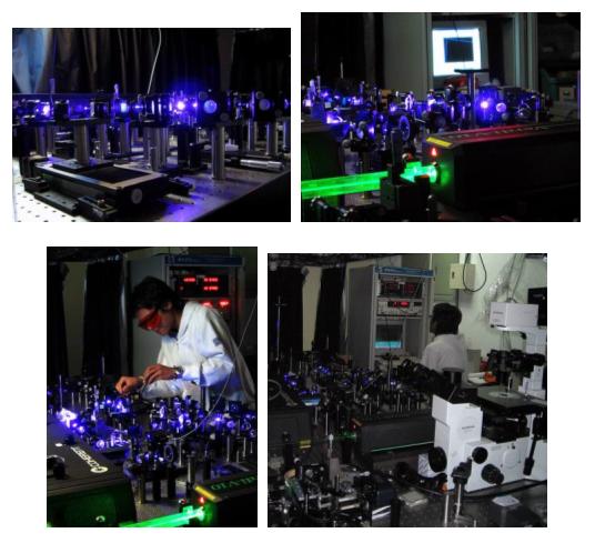
The atomic force microscope (AFM), just like a human finger, can “sense” the surface morphology and “feel” the stiffness of materials with a nanometer spatial resolution. The near-field optical microscope, on the other hand, can resolve the nanoscopic spatial distribution of optical fields with a tapered fiber tip. Combining these two apparatus and femtosecond laser pulses, we can perform experiments and obtain imaging with high spatial (nanometer) and high temporal (femtosecond) resolutions. Under the funding of National Science and Technology Program for Nanoscience and Nanotechnology, we are currently conducting related researches. Topics include: (1) carrier and phonon dynamics of nanoparticles, (2) High spatial and temporal resolution of nano-ultrasonics with the aids of optical second and third harmonic generations.
2. Nano-ultrasonics
Acoustic waves have been wildly utilized for applications such as sonar and ultrasonic imaging. However, the frequency of acoustic waves for typical applications is less than 1GHz, and the corresponding wavelength is longer than 1 mm. Consequently, nanometer resolutions can not be achieved by low-frequency ultrasound. Recently, we have successfully generated acoustic waves with a wavelength shorter than 10 nm, which are phrased as nanoacoustic waves or acoustic nanowaves. In solids, this acoustic wavelength is only as long as tens of atom spacing and the acoustic frequency is up to the THz regime. For acoustic waves with such a short wavelength and high frequency, their physical properties are intriguing and we are investigating several physical issues related to nanoacoustic waves, such as propagation loss, scattering, and dispersion.
Generation of nano-acoustic waves not only opens the passage to a new field but also creates the possibilities for innovative applications and technologies in the future. In respect of applications, we have studied phonon mirrors (which are made from phononic bandgap crystals) that selectively reflect nanoacoustic waves at specific frequencies. Besides, we have demonstrated frequency-tunable nanoacoustic waves in the sub-THz regime by optical coherent control techniques. Furthermore, we have also demonstrated that nanoacoustic waves can be utilized for ultrasonic nanoimaging. This developing nanoultrasonic technique has the advantages of non-destructive measurement, three-dimensional sub-surface imaging capability, and nanometer resolutions, of which other state-of-the-art imaging technology does not possess all. Nanoultrasonic imaging technology has great potential for nondestructive investigations of three-dimensional nanostructures, elasticity in the nanometer domain, and the forth.
 |
|
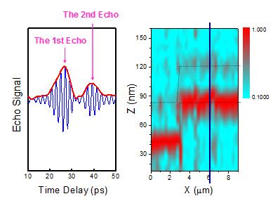
Figure 1:The nanoultrasonic imaging technology is based on a “pulse-and-echo” method to examine the subsurface nanostructures. As shown in the left figure, two echoed peaks correspond to the echo time from different interfaces in the samples to be examined. From the information of sound velocities and echo time, we can nondestructively obtain the subsurface structures of the sample as shown in the right figure. |
3. Nano-particles and nano-plasmonics
When material dimension reduces to the sub-micron or even to the nanometer regime, its optical and material properties would behave much differently. This nano-effect creates new application possiblilities and rooms for optimization.
Currently we are conducting research on the nonlinear optical properties and acoustic behavior of quantum dots and nanoparticles. In quantum dots, quantum confinement effects can be observed because of their size; their discrete energy levels, their optical and acoustic behaviors when doped in different matrices are one of the topics we are intensively studying. In nanoparticles, their ratio of surface to volume is much larger than their bulk counterparts and their sizes are on the same order of or less than the optical wavelengths; consequently resonance, magnification and other behaviors of electric fields on their surfaces can be evidently observed and a research field called “plasmonics” is established. We are conducting experiments on nanoparticles of metal, alloy, composite materials and biological molecules, aiming to decide their properties of higher-harmonic generation and to evaluate them as contrast agents for biophotonic applications.
 |
|
Figure 2:The third harmonic generation (THG) ratio of silver nanoparticles at different THG wavelengths (in solid squares) and the theoretical curve (in solid line). The inset shows the χ(3) value of Ag nanoparticles calculated from experimental data at different excitation wavelengths. |
4. Nano-biophotonics and nano-toxicology
Recently, nanotechnology has been widely used in many commercial products in daily life. In our lab, we are trying to deliver metal nanoparticles and quantum dots into cells as contrast agents. Compared with traditional staining, using nanoparticles or quantum dots can avoid photo bleaching effects. On the other hand, toxicity of these applied nanoparticles has gradually become a serious issue. Through collaboration, we are also conducting nano-toxicology studies on specific nano-particles. These studies could provide answers to future nano-medicine.
(2) Biophotonics:
1. Nonlinear optical microscopy
Compared with traditional reflection/fluorescence confocal microscopy, nonlinear optical microscopy can avoid out-of-focus photodamage and is with an intrinsically three dimensional sectioning capability. Combined with a laser source with an emission wavelength at the biological penetration window (1200-1300nm), it can further reduce photodamage and increase the penetration depth in live biological specimens. In our lab, we focus on the development of multimodal nonlinear microscopy combining second harmonic generation (SHG) and third harmonic generation (THG) signals, while minimizing the usage of multi-photon fluorescence signals. SHG microscopy is generally used to observe non-centrosymmetric structures, THG microscopy is generally used to provide morphological information, and multiphoton fluorescence microscopy is generally used to provide molecular images. In our previous nonlinear optical microscopy studies of in vivo vertebrate embryos based on a femtosecond Cr:forsterite laser with a central wavelength at 1230nm, complex developmental processes throughout the 1.5-mm-thick zebrafish embryos from initial cell proliferation, gastrulation, to tissue formation could all be continuously visualized in vivo without any treatment on live specimens. We also demonstrated the first in vivo optical virtual biopsy based on epi-THG microscopy using Syrian hamster oral mucosa as a model system. Without complex physical biopsy procedures, epi-THG microscopy can provide high-spatial-resolution dynamic images of oral mucosa and sub-mucosa in all three dimensions. The demonstrated intravital epi-THG microscopy provides high resolution observation of blood flow in capillaries and could be a promising tool to image angiogenesis, which is an important feature of many human diseases including malignancies. We also demonstrated the first four photon fluorescence microscope.
|
|
|
Figure 3:An example movie of in vivo horizontally sectioned epi-THG microscopy shows the blood flow in the capillary (indicated by blue arrow) in the sub-mucosa layer of the hamster oral cavity. Image size: 80 × 80µm. Red: THG; Green: SHG. |
2. Nonlinear endoscope
An endoscope is an important tool for noninvasive medical diagnosis. For future clinical applications, we are trying to set up several nonlinear endoscopes based on near-IR nonlinear microscopy that has 3D sub-micron resolution and high penetration in bio-tissues, including fiber-bundle-based and MEMS-mirror-based endoscopes. The project is sponsored by the National Health Research Institute.
|
|
|
Figure 4:Fiber-bundle-based nonlinear endoscope. The image resolution is determined by the distance between two adjacent cores. The scanning mechanics can be put on the opposite end of the bundle so that the entire optical system at the sample end can be made very small. |
3. Optical molecular imaging
Optical molecular imaging is a technique that combines optical microscopy with molecular biology techniques to in vivo observe signal transmission, gene expression, and so on. Our laboratory collaborates with the Institute of Molecular and Cellular Biology, National Taiwan University, to develop a new kind of transgenic fluorescent zebrafish, which can be two-photon excited by our infrared femtosecond laser. Combined with harmonic optical microscopy, tracking the embryonic development of zebrafish heart in vivo and noninvasively can be achieved. We also collaborates with National Taiwan University Hospital and National Cheng Kung University Hospital to develop various nanoparticles, which can be used to in vivo target certain molecules or genes to enhance harmonic signals, that is, to act as the contrast agent of harmonic signals. In the future, our laboratory will keep developing techniques like FRET, FLIM techniques, etc., and our final goal is to apply these techniques for clinical applications and to provide useful information for clinical diagnoses.
|
|
|
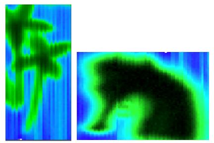
Figure 5:The images of zebrafish heart obtained from a live 30-hpf zebrafish. Since this was a transgenic fluorescent zebrafish, red two-photon-fluorescence can be excited by our home-built infrared femtosecond laser and be found in cardiac cells (Fig. (a), shown in red color). Moreover, second harmonic generation reveals the cardiac muscle (Fig. (b), shown in green color), while third harmonic generation shows the sketch of the cells (Fig. (c), shown in blue color). Figure (d) shows the combined image of (a) and (b); figure (e) shows the combined image of (a) and (c). Image size: 60 × 60mm. |
4. Gene engineering and stem cell research
A stem cell is a non-specialized, generic cell that can make copies of itself and differentiate into specialized cells for various tissues in the body. Collaborating with NTU Center for Genomic Medicine, our lab is in charge of the optical imaging system and participates in many gene engineering and stem cell researches. We have observed the development of pluripotent stem cells and neurons after the gene function was blocked.
5. Noninvasive early diagnosis of cancers
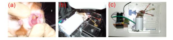
Cancer is the first cause of death in the past 23 years in Taiwan. If cancer can be diagnosed as early as possible, the death rate can be significantly reduced. In the past, physical biopsy is traditionally recognized as the final standard tool to diagnose cancer. However, physical biopsy requires removal, fixation, and staining of tissues, cells, or fluids from the lesions of patients. Such histological procedures are not only time-consuming but also invasive and painful. In addition, traditional physical biopsy procedures per se may potentially put patients in the risk of spreading tumor cells. Moreover, unless tedious serial sectionings are performed, there is no guarantee for a missing diagnosis due to a local invasion not present in the given histological sectioning examined by the pathologists. Therefore, a non-invasive in vivo optical virtual biopsy, which can provide highly penetrative three-dimensional (3D) images with a sub-micron spatial resolution to assist the real physical biopsy, is highly desired. In our lab, we developed nonlinear optical microscopy including SHG, THG and multi-photon fluorescence microscopy to study morphological and molecular differences between cancerous and normal tissues. The following figure shows one example that we use nonlinear optical microscopy to study oral cancer in a hamster.
|
|
|
Figure 6:(a) Induced oral tumor in the hamster oral cavity. (b) After anaesthetization, the hamster oral tumor was studied by our nonlinear optical microscopy. (c) The hamster was rested in a system that can maintain the vital signs and the body temperature of the test animal. |
(3) Ultrahigh frequency photonics:
1. Ultrahigh speed optical communication and photodetectors
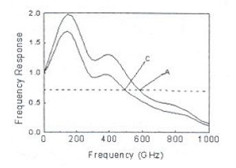
In applications of ultrahigh-speed communication systems, photodetectors with high power-bandwidth products play an important role in photoreceiver circuits or in sub-millimeter wave signals generation. Our group has devoted to developing high-bandwidth and high-power photodetectors, while our photodetectors achieved a record-high electrical bandwidth (570GHz) and a record power-bandwidth product as large as 5.7 THz-V. Currently we are developing higher output power and higher bandwidth photodetectors by using all sorts of nano-optics effects.
|
|
|
Figure 7:Frequency response of a low-temperature-grown GaAs metal-semiconductor-metal traveling wave photodetector (LTG-GaAs MSMTWPD) under the excitation light of different average power (A:1mW;C:2.2mW). Our photodetector displays a record high electrical bandwidth of 570GHz under 1mW excitation light. With short carrier trapping time of LTG-GaAs and superior microwave performances such as lower high-frequency microwave loss, higher microwave velocity, and better impedance matching between external loads and TWPDs, these MSMTWPDs also achieve excellent power-bandwidth product performances. |
2. Terahertz photonic transmitters
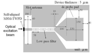
Terahertz (THz) waves are defined as electromagnetic or optical waves at frequencies ranging from 100 GHz to 10 THz. THz waves can be applied to ultra-high speed communication systems, molecular spectral imaging, national defense security, and other various novel applications. Currently generation of THz waves is still a challenge and we have successfully developed various THz photonic transmitters based on existing processing technologies. With the support of National Science Council in Taiwan, we successfully developed THz transmitters that can generate tunable THz waves at room temperature and are also easily integrated with other semiconductor devices. Moreover, our proposed device attains a record-high light-THz power conversion efficiency of 0.33% at 404.5 GHz and is the first optical device with an equivalent external quantum efficiency over 100%. Collaborating with Prof. Reey-Bei Wu of Graduate Institute of Communication Engineering, we are now developing THz antenna array technologies.
|
|
|
Figure 8:Top view of a THz photonic transmitter. Geometric information of the device is provided. We pump the optical excitation beam into the front edge, with an edge-coupled MSMTWPD, and the photo-generated current transmits through the coplanar waveguide to the slot antenna and radiates THz waves out. Behind the antenna is a low pass filter designed to avoid high frequency AC signals leaking into the DC probe pad in order to increase radiation efficiency at high frequency. |
3. Terahertz fiber systems
In the past twenty years, scientific investigations on terahertz phenomena were intensively conducted based on the rapid developments of terahertz generation and detection techniques. However, most of today's THz setups still feature planar or curved metal reflectors. Such setups are rigid and vulnerable to environmental disturbances. We keenly need a suitable terahertz waveguide for more advanced THz applications.
We proposed and demonstrated a subwavelength PE fiber for terahertz wave guiding. This makes THz waveguiding more controllable, reliable and flexible compared with free-space propagation. The only sustained HE11 mode will allow a large portion of energy outside the fiber and thus the THz wave propagates with a low attenuation constant on the order of or less than 0.01 cm-1. Besides, the measured free-space coupling efficiency of the fiber is up to the order of 20% by using an off-axis parabolic mirror. With this direct coupling capability, our proposed THz fibers can be easily integrated with current THz systems.
4. THz microchip and biosensing
Sensing devices designed to identify minute amounts of biochemical substances accurately and noninvasively are strongly desired for many applications, such as in lab-on-a-chip (or biochip) development. Current analytic methods, including fluorescence based techniques, require modification of the surroundings of molecules and thus disturb the nature of the target molecules and could lower the precision of detection. Besides, it could increase additional preparation steps of sample testing. One alternative without disturbance of target molecules is the terahertz (THz)-based biosensing technique. Based on molecular fingerprints, direct THz-probing is a sensitive, label-free, and noninvasive way for biomolecule detection.
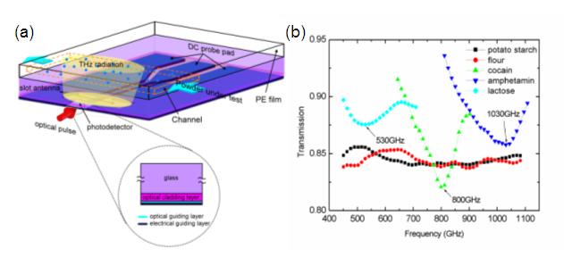
For the first time, we directly integrated an optoelectronic micro-THz source into a glass-substrate microchip for direct, sensitive and localized sensing of biomolecules, which are preserved in their native states. The capability to identity different illicit drug powders based on their spectral characteristics was successfully demonstrated with a < 10 nano-gram sensitivity. This THz microchip system has the advantages of label-free detection (needs no probing molecules), high selectivity (based on spectral characteristics of molecules), no sample preparation, repeatable usage (just replace the PE film), and ease of parallel integration with other biochip functionality modules, which are desirable for future lab-on-a-chip applications. Our demonstration shows the possibility to integrate optoelectronic-based photonic transmitters with current biochip technologies for various biosensing applications, including DNA sequencing and detections of explosive and virus. Due to the unique capability to detect the biomolecules in their natural states, the THz biochip should also enable future studies of molecular conformational dynamics.
|
|
|
Figure 9:(a) The schematic diagram of the proposed THz- biosensing chip with a size of 1 × 1 mm. The top part is the glass- substrate polyethylene (PE) sample cell with hot-embossed 20µm-deep channels where sample powders were contained. A broadband THz photonic transmitter was inversely integrated in the bottom of the 150-µm-thick glass substrate. By placing the molecules to be detected within the near-field distance of the micro-THz source, localized detection can be achieved and has the potential in multiplexing for future array applications. (b) THz micro-absorption spectra of 5 different white powders tested, acquired by the THz microchip system. Two of them are illicit drugs: cocaine and amphetamine. With weight on the order of nano-grams, the characteristic absorption peaks of cocaine and amphetamine at ~800 GHz and ~1030 GHz can both be clearly identified, in sharp contrast to potato starch, flour, and lactose powders. |
5. THz molecular imaging
Many molecules have resonant absorptions at the THz spectral range and thus can be distinguished. Based on these molecular fingerprints, THz EM waves are used for imaging molecular distribution that can be applied to detection of virus and explosives hidden in plastics. Our recent research is devoted to the combination of compact THz photonic transmitters and THz subwavelenth fibers to realize a THz molecular imaging system with a miniature size, such as a THz endoscope system.
|
|
|
Figure 10:Our demonstrated THz biomolecular images. THz waves could transmit through opaque objects and reveal hidden bio-molecule distributions. The left figure shows the THz image of a fresh flower at 945GHz, where the dark part reveals the distribution of water molecules. The right figure shows the THz image of a dried seahorse at 1 THz, where the dark part is the distribution of protein molecules. The measured images do not require exogenous contrast agents and this T-Ray image system has high potential for future clinical and national security applications. |
(4) Femtosecond optics:
1. Femtosecond laser
Femtosecond lasers can generate optical pulses with a duration on the order of 10-15 seconds. It’s an important tool for the studying of ultrafast phenomena. In our lab, the operating femtosecond lasers include two home-built Cr:forsterite mode-locked lasers, three commercial Ti:sapphire mode-locked lasers, and one commercial optical parametric oscillator (OPO).
The operation wavelengths of Ti:sapphire lasers range from 700 to 1000nm. The typical output power is 1.5W with a shortest pulse width of 30fs and a highest repetition rate of 2GHz. By frequency doubling with nonlinear crystals, blue or UV femtosecond pulses can be achieved from 350nm to 500nm. Combined with the OPO, the operation wavelengths of femtosecond pulses can be extend to 1 ~ 2mm.
The home-built Cr:forsterite lasers operate around 1230nm with a 100fs pulse-width. At a 110MHz repetition rate, the output power could be as high as 300~500 mW. We successfully shrank the size of cavity through the use of double-chirped mirrors. Based on this system, Cr:forsterite lasers became more portable and could be widely applied to medical uses. In the future, our lab plans to build more portable Cr:forsterite femtosecond lasers with higher output power.
2. Ultrafast laser fields diagnostics
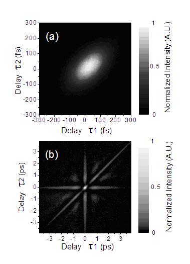
For ultrafast optical pulses, which are typically 100 femtosecond in duration, the variation of fields is faster than the speed of electronics. To obtain the complete field information, including amplitude and phase, we have developed a technique called "Triple-Optical Autocorrelation for Direct pulse shape measurement (TOAD)". From the measured triple-autocorrelation function by third-harmonic generation, we can analytically calculate the temporal shape of pulse intensity and uniquely determine the phase by a spectral measurement with Gerchberg-Saxton algorithm.
|
|
|
Figure 11:Third-harmonic-generation based triple-autocorrelation of laser pulses. According to the measured data, we can directly obtain the filed intensity in the time-domain without any iterative algorithm. |
3. Photonic-crystal-fiber-based ultrafast source
Optical laser beams can be confined and guided within a small area by a photonic crystal fiber. When the optical intensity is getting higher and higher, the third order nonlinear effects such as self-phase modulation will appear. Balancing this effect with the dispersion of material, optical solitons can thus be formed, which can keep the pulse width unchanged for a long propagation length. In our lab, exploiting the self-frequency shift induced by optical soliton and Raman scattering effects, 800nm~1600nm ultrafast sources can be obtained by the excitation of 800nm femtosecond pulses from the Ti:sapphire laser. The wavelength can be tuned through the polarization of excitation, thus providing femtosecond sources with a broad tuning range. Under the funding of National Science Council and National Health Research Institute, our lab is now studying the ultrafast phenomenon of photonic crystals and planning to apply them to biology researches and optical control of pulse propagation.
4. Ultrafast carrier dynamis of wide-bandgap light-emitting semiconductors
The dynamic characteristics of carriers in semiconductors play an important role in the performance of the electronic and optoelectric devices. We use femtosecond-laser techniques to study the carrier dynamics within an ultrashort time domain, such as carrier-phonon interactions, radiative recombination processes from a signal quantum well, room-temperature exciton dynamics, and carrier dynamics in bandtail states. Besides wide-bandgap semiconductors such as GaN and ZnO, recently we also focus on the carrier dynamics in infrared materials such as InN.
|
Display Optics Laboratory In the one-and-a-half year-old Display Optics Laboratory, we are aiming on developing the optical technologies for display applications. We are focusing on designing and fabricating novel optical elements and systems for improving the performances of several different displays. For example, we use microlens arrays to enhance the light extraction efficiencies of solid state light emitting devices, e.g., LEDs or OLEDs. The design parameters are systematically investigated and useful design rules are concluded for brightness enhancement of such devices. Furthermore, we have studied the effects of microlens arrays on the image quality of solid state emissive display devices. |
|
|
|
|
Power and luminance efficiencies v.s. area ratio of different microlens arrays |

We have also studied non-conventional optical elements such as gratings. An example is a color separation grating for separating different color lights into different diffraction orders. Application in display system is a high efficient color separation element for replacing the conventional color filters.
|
|
|
|
The spectrum and configuration of the color separation grating |
|

We have also studied non-conventional display systems such as auto-stereoscopic displays. An example is a large area system based on rear projection technology. We adopt two orthogonal circular polarized waves in stead of two orthogonal linear polarized ones to avoiding crosstalk effect. In such a system, we design a broadband retardation plate in order to minimize the chromatic dispersion of the system.
|
|

The above research results are accepted as four international conference papers and further results are preparing for patent filing and journal paper submission.
|
Laboratory of Fiber Laser Communications and Nano-Photonics I. Research Goal of Laboratory We concentrate our research on developing versatile specific synthesizing processes for Si nanostructures and related devices, investigating the physical mechanisms behind the material, electrical, and optical aspects of the Si nanodots, |
|
nanopyramids and nanopillars. The targets are implementing Si nanophotonic devices based on quantum confinement effect, and discuss in more detail the origin of the enhancement on radiation/detection, solar energy conversion, and surface plasmonic resonance at blue-green wavelength region. A future collaboration with Academia Sinica on the ab initio atomic potentials based boundary integral Green function for the quantum computation of Si quantum dots with atomic numbers ranging between 103-104 will be initiated to study the electrical property of Si nanocrystals. These simulations will be helpful to elucidate the carrier transport and penetration between Si nanocrystals and neighborhood dopants, and to realize the surface plasmonic wave interaction between Si nanostructures and biomoleculars. Several featured researches including ultra-low threshold ICP power PECVD synthesis for Si nanopyramids, CO2 laser based rapid thermal annealing for precipitating Si nanocrystals, rapid self-aggregated metallic nanodot array for SPR or nano-lithographical applications will be introduced in the following sections.
On the other hand, we are interested in fundamental and technical study of fiber laser schemes for potential applications on ultrafast optoelectronic diagnosis, high-speed fiber-optic communications, and biophotonic or biomedical analysis, etc. Over past years, we have constructed several types of continuous-wave and shorted-pulsed Erbium-doped fiber amplifier or semiconductor optical amplifier based fiber ring lasers. In particular, we have theoretically simulated and experimentally established an optical injection mode-locked semiconductor optical amplifier fiber laser system, which exhibits femtosecond pulsewidth after external soliton compression and facilitates high-repetitive low-supermode-noise output. The other milestones of our works include 40th-oeder rational harmonic mode-locking of EDFL using a FPLD based mode-locker, mutual injection-locked EDFL/EDFL and FPLD link, tipped fiber based low-splicing-loss fusion technology between different fibers, >10GHz backward optical injection induced cross-gain-modulation for mode-locking, etc. In brief, the distinguished researching fields on Si nanophotonics, fiber lasers, and all-optical communication data processing likes are emphasized in our laboratory, which include:
A. Femtosecond Mode-Locked Fiber Lasers and Soliton Compressors
B. Nanocrystallite Silicon LEDs and Solar Energy Photonics
C. All-Optical OC-192 NRZ/RZ Communication Data Format Processing
D. Mutually Injection-Locked Laser Diode Based Fiber-Optic Communication Link
E. Millimeter-wave Optoelectronic Phase-Locked Loops and Phase Shifters
F. GaAs:As+ Ultrafast Photoconductive Switches and Time-Resolved Optical Diagnostics
|


II. Silicon Nano-Photonics
II-1. Local Synthesis of Si Nanocrystals in SiOx via CO2 laser Rapid Thermal Annealing
Nowadays, the progressive development on Si nanostructures based photonic devices are particularly for the potential solution of novel optical interconnect between chip modules, which effectively integrate the waveguides, photonic crystal devices, and Si based electronic ICs on the same Si wafer to form a all-Si based photonic system on chip. The key component to realize the Si based optical interconnect relies strictly on the implementation of fully compatible Si light emitting devices, however, which are still not a mature product at current stage. Typically, the Si LEDs were fabricated using Si nanocrystals buried in the SiOx file deposited by anomalous PECVD and post high-temperature annealing processes. Furnace annealing at higher than 1000oC and longer than 30 minutes usually degrades or damages the adjacent ICs, which in turn making the integration of Si LEDs and ICs impractical. This urges us to seek alternative solution for locally synthesizing the Si nanocrystals in the Si-rich SiOx film, and the best candidate is the focused laser annealing process. Previously, excimer lasers, argon ion lasers, and Ti:sapphire lasers were ever employed as the common sources for annealing or refining versatile materials. Nonetheless, these lasers experiences extremely low absorption procedure in general SiOx materials, in which the optical energy is unable to efficiently convert into the heat during illumination. Therefore, the precipitation of Si nanocrystals cannot be demonstrated using these visible or near-infrared lasers. With the aid of a simulation model for three-dimensional thermal conductance, we propose for the first time the local synthesis of Si nanocrystals within SiO2 matrix by using CO2 laser based rapid thermal annealing procedure. Experimental results reveal the generation of Si nanospheres with a concentration up to 1018 cm-3 within a spot size of 50mm under a focused laser illumination intensity of 6 kW/cm2, while the Si nanocrystal size can be well controlled at 3-8 nm. The optimized laser annealing intensity is well below the laser ablation threshold, and a dehydrogenated process can also be implemented under a lower laser intensity of <4 kW/cm2. With such a CO2 laser annealed SiOx, we have successfully fabricated a MOS light emitting which exhibits similar characteristics with those fabricated using conventional furnace-annealed SiOx films.
|


II-2. Si nanocrystals Based Light Emitting materials and Diodes
We also investigate the white-light and near-infrared electro-luminescent characteristics of the MOS diodes fabricated on the PECVD grown Si-rich SiOx film on Si substrate after high-temperature furnace annealing. By changing the substrate temperature and induced couple plasma power during PECVD growth, the structure defects and Si quantum dots related PL mechanism have been studied in detail. It is further observed that numerous Si nanopyramids can be grown along the (100)-oriented Si/SiOx interface under the high substrate temperature and threshold ICP power conditions. The power-variant and temperature-variant µ-PL spectra further interpret the contribution of the self-trapped exciton located at Si quantum dot surface to the PL at 700-850 nm. It is confirmed by comparing the EL from the as-deposited and annealed SiOx films that the Si nanocrystal contributes to the EL at 650-850 nm, whereas the EL at 400-650 nm is attributed to the Si and oxygen vacancy related radiative defects such as weak-oxygen bonds, neutral oxygen vacancy, and E’δ the precursor of Si nanocrystals, etc. The preferred transport path of the injected carriers is through the defect sites, which can be avoided via the increasing substrate temperature and decreasing ICP power during growth. Such a synthesizing process also facilitates the stable near-infrared EL and lengthened device lifetime. In addition, the proposal on resonant-cavity enhanced EL device is very promising.
|


II-3. Formation and Diagnosis of Si Nanopillars on Si Substrate
In particular, we have primarily demonstrated the rapid self-aggregation of metallic nanodots on Si substrate by using a less-adhesive and heat-accumulated SiO2 buffered layer. The self-assembly of metallic nanodots on Si wafer surface spends thermal processing time up to 10s minutes in previous work, which is mainly attributed the ultra-high thermal conductivity of 148 W/m-K in Si substrate. This causes the metallic nanodots hardly to be congregated on the surface. With the deposition of a 20nm thick low-conductivity SiO2 buffered layer, the formation of NiSi2 compounds restricted and the adhesion between Ni and Si can be released, the heat can therefore be accumulated at the Ni/SiO2 interface to enhance the self-aggregation process. This eventually results in a significant reduction on the formation duration of Ni nanodots from 10s min to 22 sec. The average size and surface density of the formatted Ni nanodots are 30nm and 7´1010 cm-2, respectively. Subsequently, the Ni nanodot array is employed as a mask for generating Si nanopillars via an ICP-RIE process. The largest height-to-width aspect ratio ever obtained for the Si nanopillars in experiments is about 8-10 at a maximum height of 400 nm. After removing the Ni and SiO2 nanodots from the top of Si nanopillars, a visible PL is emitted from the Si at wavelength of 400-600nm. Weak PL at near-infrared region (~750 nm) is also observed due to the occurrence of quantum confinement effect in Si nanopillars with size <10nm. This has been verified in the experiment of saturating PL intensity with enlarging pumping power. Furthermore, the blue-shift in PL wavelength of Si nanorods due to the persistent oxidation of Si nanopillars is reported. Other effects such as faster charging/discharging, lower resistance and capacitance, and extremely low optical reflectivity are also observed.
|


III. Mode-Locked Fiber Laser Systems
III-1. 40GHz and 40th Rational Harmonic Mode-Locking Fiber Laser
By using a
1GHz loss-modulated Fabry-Perot laser diode, we have implemented the
rational harmonic mode-locking of an Erbium-doped fiber laser system. The
FPLD is not DC biased to remain unlasing condition, while a amplified RF
signal is employed to sinusoidal modulated the FPLD, which facilitates the
switching on the operation mode of the FPLD between loss modulation and gain
switching. In the proposed system, the FPLD is neither lasing nor
gain-switching, which experiences a threshold modulating power of nearly 18
dBm to initiate the mode-locking of EDFL. After a chirp compensation with
dispersion managed fiber, the EDFL pulsewidth as short as 3 ps associated
with a spectral linewidth of 1.3 nm can be obtained, corresponding to a
transform-limited time-bandwidth product of 0.31. If we denote![]() as the fundamental mode frequency of the EDFL, and define
n and p as the harmonic and rational harmonic orders of the EDFL, it is seen
that the rational harmonic mode-locking can be achieved when the modulating
frequency of the FPLD is adjusted from
as the fundamental mode frequency of the EDFL, and define
n and p as the harmonic and rational harmonic orders of the EDFL, it is seen
that the rational harmonic mode-locking can be achieved when the modulating
frequency of the FPLD is adjusted from
![]() =
= ![]() to
to ![]() =
=![]() . Therefore, the repetition frequency of the EDFL becomes
p times of the FPLD modulation frequency. Experimentally, a detuning
frequency of 113 kHz will give rise to a 40th ordered rational
harmonic mode-locking output from the EDFL, in which the harmonic and
rational harmonic orders are n=228 and p=40, respectively.
. Therefore, the repetition frequency of the EDFL becomes
p times of the FPLD modulation frequency. Experimentally, a detuning
frequency of 113 kHz will give rise to a 40th ordered rational
harmonic mode-locking output from the EDFL, in which the harmonic and
rational harmonic orders are n=228 and p=40, respectively.
|
||||


In opposite, the FPLD changes its operation function to generate gain-switched pulses when the DC biased current of the FPLD is increased to nearly threshold condition, while a dual pulse-train phenomenon revealed the such an evolution has been found during the current detuning procedure. However, such kind of mutual injection-locking induced gain-switching inevitably broadens the EDFL pulsewidth to 26.4 ps, which is almost the same as that of a typical gain-switched FPLD (~21 ps). Under such a strong competition, the mode-locking mechanism of the EDFL will be destroyed and the FPLD becomes lasing, the overall output stability of the mutually injection-locked gain-switching FPLD-EDFL link is relatively better than that of a FPLD loss-modulated rational harmonic mode-locked EDFL. This is attributed to the narrow locking range of the mode-locking effect. In addition, the unequivalent amplitude among adjacent pulse peaks needs to be eliminated using a intra-cavity Fabry-Perot etalon filter. The effect of gain depletion in FPLD on its mutual injection locking and gain switching performances was realized to corroborate the diminishment of the rational harmonic mode-locking mechanism.
|

III-2. Backward Optical Injection Harmonic Mode-Locked SOA Fiber Laser
Alternatively, we perform a novel mode-locking mechanism for the semiconductor optical amplifier (SOA) based fiber ring lasers, which employs a modulated optical source to inject the SOA for gain depletion or cross-gain modulation. By reshaping the gain window of the SOA with optical TTL signal of variable duty cycle, we theoretical simulated and experimentally demonstrate for the first time a 10GHz harmonic mode-locked SOAFL, in which the effect of cross-gain modulated gain window on the gain depletion level and the mode-locking dynamics was elucidated. Such a high-speed backward injecting optical signal can be generated by passing a directly sinusoidal modulated distributed-optical-feedback laser diode output through an optical circulator to inject the SOA. To reshape the injection optical wave and detune its duty cycle, a pseudo random binary sequence code is used to generate TTL signal for encoding the DFBLD in a traveling-wave Mach-Zehnder modulator. Furthermore, the modulator has to be biased at nonlinear level for reshaping the optical TTL or pulse into a dark-optical-comb shape. In principle, the SOA functions as a gain medium and a loss-modulator concurrently. To improve the bandwidth of SOA and prevent the saturation of circulated mode-locking pulse-train in the SOA, an appropriate output coupling ratio for high output power should be decided. Rational harmonic mode-locking output can also be obtained by slightly detuning the modulating frequency of the DFBLD. To obtain a shortened or transform-limited pulse, the dispersion compensation and soliton compression techniques are introduced. A dispersion compensated fiber loop are employed to achieve chirp-free SOAFL pulse and a high-gain EDFA is used to raise the peak power of the zero-chirp SOAFL pulse for high-order soliton generation in a single-mode or dispersion shifted fiber spool. Consequently, the wavelength-tunable SOAFL pulse-train with average power of >1 Watt and pulsewidth of <100 fs can be obtained.
|
||||


III-3. 10s Femtosecond High-Power Soliton Compression of Self-started Additive Pulse
Mode-Locked Erbium-doped Fiber Laser
To further increase the peak power of ultrashort fiber laser pulses for versatile applications, the external cavity amplifier should be configured instead using an ultrahigh-gain laser cavity. Among different approaches, the chirped amplification is a very useful technique, which induces a pre-chirp into the APM EDFL pulse via a nonlinear medium prior to the high-power amplification process, leading to a broadening of pulsewidth and a reduction in peak power and thus prevent gain saturation phenomenon. Afterwards, the pre-chirped and amplified EDFL pulse is compressed again to reach high peak power. However, the handling power-length products in conventional fibers are limited at about 1 kW×m due to their small mode fields. The value is further reduced to below 0.5 kW×m in most fiber laser source with fiber length of several meters, which makes them being inappropriate as the dispersion compensation medium. Besides, the compressed pulse quality is strongly correlated with the order of the soliton compression stage. Our approach is using a large-mode-field-area EDFA to shorten the fiber length and to suppress the nonlinear self-phase modulation effect. At last, a negative chirp is added into the EDFL pulse by passing through a segment of single-mode fiber, which compensates the positive chirp induced during the high-power amplification process and helps to continuously shorten the pulsewidth. Such an all-in-one configuration decreases the soliton order and suppresses the pulse pedestal to obtain a pure Gaussian pulse shape with peak power of 46 kW and pulsewidth of 56 fs. Extremely short pulsewidth of 30 fs can be achieved via a second-stage soliton compression process, the overall pulsewidth compressing ratio and peak-power amplification ratio are up to 10 and 700 times, respectively.
|


IV. All-Optical Communication Data Format Processing Technology
All Optical Networks (AONs) have been considered as the emerging solution for future high-speed fiber-optic communication link, which avoid the O-to-E and E-to-O transformation induced network bottleneck and establish O-to-O processing devices and techniques to overcome the speed limit of electronic carriers. On the other hand, both the Fiber to the home (FTTH) and the Radio-on-Fiber (ROF) were already selected as the potential candidates for the last mile transmission solution. The following illustration shows the configuration of AON link with backbone and ROF networks. In particular, the highly repetitive and low duty-cycle return-to-zero (RZ) optical carrier source, NRZ-to-RZ and RZ-to-NRZ transformers are the immediate work to be developed in the AON fields. To build the sub-Tbit/s pulsed optical carrier systems, we propose versatile mode-locking fiber laser configurations by using erbium-doped fiber amplifiers (EDFAs), traveling-wave semiconductor optical amplifiers (TW-SOAs), and fiber-based Raman amplifiers (FRA) as gain mediums, the self-developed novel low-loss fusion splicing technique, and the rational harmonic mode-locking technique to develop sub-Tbit/s (larger than 200 Gbit/s) fiber lasers. Broad-band wavelength tenability, timing stabilization and nonlinear pulse compression are the key issues to be developed with these systems. The construction of sub-Tbit/s all-optical diagnostic platform rely on the integration of photonic-crystal based nonlinear fiber loop mirror and 40-80GHz optoelectronic frequency regenerative system with the rational harmonic mode-locking fiber lasers. We aim to investigate novel all-optical signal processing components/sub-system and corresponding testing infrastructure, which will be employed to build up a connection with the radio-on-fiber (ROF) based last-mile transporting networks, where the microwave signal is converted into the optical signal and distributed to the remote base stations (BSs) by fiber links.
 |
Initially, a Fabry-Perot laser diode (FPLD) based all-optical data format transformer has be demonstrated for the first time, which can convert a >10 Gbit/s (OC-192) non-return-to-zero (NRZ) formatted data-stream into a return-to-zero (RZ) formatted data-stream. The implementation of the FPLD-based NRZ-to-RZ data format converter helps to increase the transmission data rate between metropolitan area networks (MAN) with the integration of passive time-division-multiplexing (TDM) technique. The FPLD-based NRZ-to-RZ data format converter will be used to link the AON and the ROF networks. Meanwhile, the optical clock-data recovery of such a RZ-formatted data-stream will be achieved using a home-made semiconductor-optical-amplifier based fiber-ring laser system, some innovative architectures will be demonstrated to implement OC-768 (40 Gbit/s) all-optical data format conversion, logic or decision gate, injection-locked 3R regenerators, etc. Our future goal will also involve the development of >200 Gbit/s high-speed pulsed optical carriers for high-bit-rate all-optical sampling test-bed.
|
|||||


Please send any comment to eoe5@cc.ee.ntu.edu.tw
Copyright
Graduate Institute of Electro-Optical Engineering, National Taiwan University