News Activity Special Report Visiting Professor Profiles Laboratory Descriptions
![]() New
faculty
members of the Graduate Institute of Electro-Optical Engineering∼
New
faculty
members of the Graduate Institute of Electro-Optical Engineering∼
Three professors joined our Institute since February 1st, 2006. Below is a short introduction to their experiences and expertise.
|
Position |
Name |
Education |
Experience |
Expertise |
|
Professor |
Sheng-Lung Huang |
Ph. D., University of Maryland, U.S.A. |
1. Director, Institute of Electro-Optical Engineering, National Sun Yat-Sen University, Apr. 2003 - Jan. 2006
Engineering, National Sun Yat-Sen University, Feb. 1999 - Jan. 2006
Optical Engineering, National Sun Yat-Sen University, Aug. 1993 - Jan. 1999 |
Research of applications of crystal fibers in optical telecommunication, nano electro-optical engineering, biophotonics; diode-laser pumped solid-state lasers, optical coating technology |
|
Assistant Professor |
Snow H. Tseng |
Ph. D., Northwestern Univ., U.S.A. |
1. Postdoctoral Research Fellow, Department of Electrical and Computer Engineering, Northwestern University, IL, USA Jun. 2005 - Nov. 2006 2. Postdoctoral Research Fellow, Department of Physics, University of Illinois at Urbana- Champaign, IL, USA Nov. 2005 - Feb. 2006 3. Research Assistant, Computational Electromagnetics Laboratory, Northwestern Univ., Sept. 1999 - Jan. 2006
Biophysics Division, Lawrence Livermore National Laboratory, USA Jun. 2002 - Sept. 2002
Computer Science Laboratory, Sony, Tokyo, Japan, Jun. 2001 - Aug. 2001
Grumman, Rolling Meadows, IL, USA Jun. 2000 - Sept. 2000 |
Simulation of optical systems |
|
Assistant Professor |
Yun-Li Li |
Ph. D., Rensselaer Polytechnic Institute, U.S.A. |
1. Process Integration Manager, Formosa Epitaxy Inc., May 2005 - Jan. 2006 2. Project Manager, Elite Optoelectronics Inc., May 2004 - Apr. 2005 3. Visiting Research Scholar, Rensselaer Polytechnic Institute, Future Chips Constellation, Jan. 2004 - Apr. 2004 |
Design and fabrication of solid-state white-light sources |
|
Currently, there are 32 full-time faculty and 300 graduate students in this Institute. Due to the busy affairs of the Institute, a Vice-Chairman is appointed. Professor Sheng-Lung Huang had been the Chairman of the Institute of Electro-Optical Engineering at National Sun Yat-Sen University for 3 years and is familiar with administrative matters. When being a part-time Professor with us, he actively participated in the affairs and understood well the current state of our Institute. Professor Huang’s outstanding research results, his enthusiasm, and strong ability in handling administrative affairs make him the best candidate for the Vice-Chairman. |
 |
![]() Workshop on Photonic Crystals and Nano-Photonics
Workshop on Photonic Crystals and Nano-Photonics
Time: November 4th , 2005 (afternoon) and November 5th, 2005 (all-day)
Place: Room 101, Barry Lam Hall, National Taiwan University
About the Workshop
The Workshop on Photonic Crystals and Nano-Photonics was held from November 4th (afternoon) to the 5th (all-day) at Room 101, Barry Lam Hall, NTU. Sponsored by Japan’s IEICE (The Institute of Electronics, Information and Communication Engineers), two internationally renowned speakers, Dr. Kiyotoshi Yasumoto (Department of Computer Science and Communication Engineering, Kyushu University, Fukuoka, Japan) and Dr. Masaya Notomi (Photonic Nanostructure Research Group, NTT Basic Research Laboratories, Atsugi, Japan), were invited to lecture on special topics. Moreover, 14 local scholars and experts of related fields presented their outstanding research results.
Participants to the workshop had been originally estimated to be around 150. With the enthusiastic participation from all fields, the final number of international and local scholars and experts reached 291. The workshop induced various discussions and fruitful results.
|
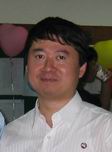
Dr. Kiyotoshi Yasumoto |
Dr. Masaya Notomi |
![]() Workshop on Advanced
Electro-Optical Technology and Education
Workshop on Advanced
Electro-Optical Technology and Education
Time: December 23, 2005 (Friday)
Place: Room 101, Barry Lam Hall, National Taiwan University
Speakers:
Dr. Yung S. Liu (Opto-Electronics Systems Laboratories, Industrial Technology Research Institute)
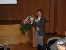
Professor Ming C. Wu (Department of Electrical Engineering and Computer Sciences, University of California at Berkeley)
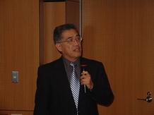
Professor Yung-Jui Chen (Department of Computer Science and Electrical Engineering, University of Maryland, Baltimore County)
Professor Shin-Tson Wu (College of Optics and Photonics, University of Central Florida)
Professor Keh-Yung Cheng (Department of Electrical and Computer Engineering, University of Illinois at Urbana-Champaign)
About the Workshop
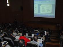
The Workshop on Advanced Electro-Optical Technology and Education was held on December 23, as a prelude to the biennial Advisory Committee Meeting. Five well-known international and local scholars were invited to give lectures. Dr. Yung S. Liu from the Opto-Electronics Systems Laboratories of the Industrial Technology Research Institute spoke on “Semiconductor Lighting - Technologies and Future Challenges”. With the prospering technological developments in semiconductor light-emitting elements, high effective light-emitting is the foremost advantageous quality. The future trend is to develop semiconductor light-emitting elements into common illuminating/lighting or display apparatuses, including indoor light sources, headlights, and display panels. Currently, the cost of manufacture is an obstacle. It is expected that after lowering the cost, light bulbs and fluorescent lights could be replaced by semiconductor light-emitting elements.
The second speaker, Professor Ming C. Wu from UC Berkeley, spoke on the “New Trends in Optical MEMS”. A few years ago when the optical fiber communication market was doing well, researches on optical MEMS focused on optical-communication switches. However, as the market withered, research has taken another direction toward developing CMOS compatible nano-opto-electro-mechanical systems or biophotonics. The fruits of this research area include the micro-disk resonators and optoelectronic tweezers by Professor Wu and his research team.
Professor Yung-Jui Chen of University of Maryland spoke on “Future Directions of Planar Lightwave Circuits”. Planar Lightwave Circuits (PLC) is the core technology of photonic integrated photonics and integrated optoelectronics and its application could be extended to photonic communications networks, optical interconnects, and detectors. The key for PLC technology to stride toward large-scale integration are high-contrast refractive-index waveguide materials and adequate platforms.
Professor Shin-Tson Wu of University of Central Florida spoke on “Tunable Photonic Liquid Crystal Devices” and stressed the tunable-focus liquid crystal microlenses and their arrays. He and his research team employed special techniques to implement polarization-independent microlenses.
Lastly, Professor Keh-Yung Cheng from University of Illinois at Urbana-Champaign spoke on “Hyper-Uniform Nanophotonic Technologies for Ultra-Fast Optoelectronic Systems”. When used in optical communications, the traditional directly-modulated laser diodes, have modulation frequencies up to only 30 GHz; the most critical limiting factor comes from the rates of current injection and electron-hole recombination. The goal of Professor Cheng’s research team is to use high-speed (direct-modulation frequency reaching THz) light-emitting transistor (LET) as the basis for constructing optical interconnect systems faster than 50 GHz.
 |
 |
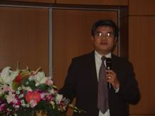 |
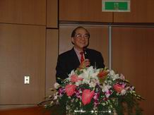
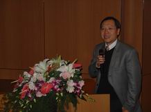
| Dr. Yung S. Liu | Prof. Ming C. Wu | Prof. Yung-Jui Chen |
 |
 |
 |
| Prof. Shin-Tson Wu |
Prof. Keh-Yung Cheng |
![]() 2005
GIEOE Advisory Committee Meeting
2005
GIEOE Advisory Committee Meeting
Time: December 24, 2005 (Saturday)
Place: Room 201, Barry Lam Hall, National Taiwan University
Counseling Committee:
Dr. Yung S. Liu (Opto-Electronics Systems Laboratories, Industrial Technology Research Institute)
Professor Ming C. Wu (Department of Electrical Engineering and Computer Sciences, University of California at Berkeley)
Professor Yung-Jui Chen (Department of Computer Science and Electrical Engineering, University of Maryland, Baltimore County)
Professor Shin-Tson Wu (College of Optics and Photonics, University of Central Florida)
Professor Keh-Yung Cheng (Department of Electrical and Computer Engineering, University of Illinois at Urbana-Champaign)
Vice Administrative Manager Bo-Yan Lu (AUO)
About the Meeting
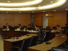
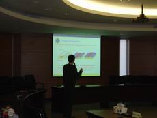
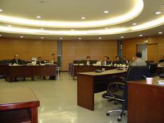
During last year’s Christmas Day, cool but nice weather replaced the harsh winds of earlier days. The biennial GIEOE Advisory Committee Meeting was held in Room 201, Barry Lam Hall. Six renowned international and local scholars and experts were invited as advisory committee members to give valuable administrative and research suggestions to our Institute. 21 enthusiastic professors from the Institute attended the meeting, giving presentations on their research, and consulted with the committee members. The entire meeting started from 9 am and lasted until 9 pm. The successful meeting demonstrated the fruits of the Institute’s research in the past two years and brought the year to a wonderful ending.
At the opening of the committee member meeting, President Si-Chen Lee and Dean Bing-Huang Chiang of Academic Affairs took time off their busy schedules to address us. Chairman C. C. Yang reported on the current state and gave a summary introduction to the Institute. Besides the research presentations by the individual professors, time was allotted for faculty members and student representatives to interact with the committee members, allowing the professors and students to raise their opinions and all concerns. After the exchange of comments among the committee members, Dr. Yung S. Liu, the Chair of the committee, summarized the suggestions by giving a brief. The meeting consummated a nice conclusion.
 |
 |
 |
Introducing the Creative Exhibition Center of Image Display Technology
![]()
By Professor Jian-Jang Huang, Ms. Hsiao-Ping Chou, and Ms. Li-Chen Tseng
With the coming and going of the PC generation, post-PC generation, internet generation, post-internet generation, the 21 century is undoubtedly the era of consumer electronics. As mp3 players, 3G cell phones, and flat-panel displays become the hot items of the 3C market and indispensable image-display interfaces, the creativity of image display and the combination of other consumer electronics gradually become issues that concern everyone.
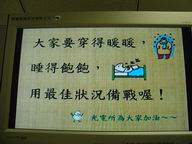
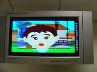
In the middle of 2005, under the direction of Chairman, Prof. C. C. Yang, we began planning for the Creative Exhibition Center of Image Display Technology. This project was subsidized by the “Image Display Technology and Talent Fostering Project” of the Ministry of Education. BenQ, AUO, and Quanta Display Inc. donated 11 32-inch TFT-LCD television sets, which have been installed in the Electrical Engineering Building II, Barry Lam Hall, and Detian Hall to play digital image contents during class time.
The displayed contents can be divided into the following categories: 1. department- and college-related activities and student activities; 2. introduction of new technologies; 3. interesting images, pictures, and animations; 4. English lessons; 5. news and weather forecast; 6. health-related issues. We welcome staff and students from the College of Electrical Engineering and Computer Science to provide information on activities and quality programs, and to comment on the aired programs.
 |
 |
 |
|
Farewell of Prof. Silvano Donati and Mrs. Donati to GIEOE When I accepted to come and spend a semester of Visiting Professor at the GIEOE, I got only a vague idea of Taiwan. At that time, I was a professor that, after having worked hard for 20-year to grow up my Group of researchers in Electro-Optics, had suddenly decided that it was time to escape the routine and devote some time in expanding my cultural horizon. More than the US, for me it was the Pacific Rim the best place to go and try to understand what is new in the world and where the world is going and why. Taiwan, this |
|
|
small island where a population of half the Italian is packed, holds a leadership position in the high-tech manufacturing of electronic products, and thus it strongly attracted me and my wife Tiziana, an electronic engineer, like me very curious about R&D issues and industrial management. So, like novel Marco Polo’s, we packed our books and headed to Taipei, where Professor C.C. Yang was offering to me a Visiting position for a semester. While I was delivering my lessons on Guang-Dien-Yi-Che (Electro-Optical Instrumentation) at the GIEOE of the National Taiwan University, Tiziana sat patiently in the office collecting and organizing her notes for a book she had in mind since a couple of years but had no time to pursue, on RF-ID and Wireless Networks Microsystems. What a surprise for her, when we drop to the underground the first time, to discover that RF-ID where already in use there, while it is just being planned in Italy! By the way, the Taipei MRT is really fine, it is probably one of the best we have seen in the world, because fast, clean and cheap. For me, a nice surprise was getting a class of Master and PhD students, sharp and bright, very interested in my lessons and not losing a word of my lessons despite the language barrier, a barrier that I never realized enough until being confronted with trying to speak Chinese words! About languages, we appreciated a lot finding English language signs in the road and in the MRT, and we owe congratulations to the municipality of Taipei for that. Also, the effort to teach English as a second language for Taiwanese is very commendable. Nowhere in other Asian Country common people in the road understands English so well. Also, the level of English speaking of students and educated people is really quite high, even better than in many European countries. Another pleasant discovery we got, early upon our arrival in September, was Confucius Day. Expressing gratitude to the elder scholars who takes care of the education of you or of your children is a sign of great and fine civilization, something that is sadly fading away in Europe on the wave of criticism to establishment and hierarchies. Along the same way, the ‘core values’ signs I saw in the Department are reminders of behavior style that fits very well in a model of society respectful of ‘good moral values’, a pleasant rediscovery for us European used to live with the ‘politically correct’ and its distortions. Also very appreciated by us was the level of personal safety around the town, as well as the good manners in the behavior of both adults and children. As we have understood after a brief brainstorming, all the above come from the mental attitude of Asian people, because it is an easy consequence of values like ‘have a peaceful mind’ and ‘stay in harmony with the world surrounding you’. And really, as European, we realize how precious these simple words are. About my teaching, it went on plain and easy, thanks to the aid and the feedback of Cheng-Yen (Robert) Chen, my teaching assistant. He patiently sat at my lessons listening carefully and signaling to me when to slow down, and when to complement the topics covered with a ‘back-to-basic’ excursus. He also planned with me the midterm and the final examination problems, and helped in reviewing and evaluating the exams. During my classes, while I have not interacted so much with Professor C. C. Yang, the Chairman of the GIEOE, I felt his constant presence, because his Swiss-clock organization of the Institute was the clue for a smoothly running activity. And also the GIEOE office, with Mr. Wu, Angela, Li-Chi, Karen and Effie were all supportive and wonderful in turning each problem into easy matter. I learned that, during the years, the Institute has grown in number of students and has attracted a lot of new Professors with very high qualification. So I think that I shall heartily thank Professor Yang for the excellent environment he has been able to create around us in the Institute. Another rising star that I met with great pleasure is Professor Sheng-Lung (Luke) Huang, formerly at the Sun Yat Sen University in Kaoshiung and now with the GIEOE. As a Chairman of the Taiwan IEEE-LEOS Chapter, I met him and had the opportunity to become acquainted with his cutting-edge research on crystal fibers. Other Professors that I knew at the GIEOE and I had a great pleasure to discuss science with, include Hung-Chun Chang, Guo-Dung Su, Lung-Han Peng, Chi-Kuang Sun, Jiun-Haw Lee and Jui-Che Tsai. Last but not least, the Dean of the EECS College, Prof. Soo-Chang Pei, was proactive in letting me understand similarities and differences of the Taiwan University organization compared to the Italian. On her side, my wife Tiziana was interested in the techno-economical structure of the many Companies operating in electronic manufacture in Taiwan. A big surprise to us, opening a daily newspaper like the Taipei Times, was to find listed in the bond quotation page, more companies in electronics than we have in Italy! So, she (and me too) tried to analyze the reason of this success. The result, after a period of visits, data collection and interviews, was an article entitled ‘Alta Tecnologia e Ricerca in Taiwan – il Miracolo Economico’ (High Tech and Research in Taiwan: the Economic Miracle) which is going to appear on the official Magazine of the Italian Electronic Engineer Association (AEIT). Indeed, the situation in Taiwan today resembles that of Italy after the World War II, when the infrastructures of the country were seriously damaged, but people were eager to reconstruct and restart the economy, which got a so wonderful takeoff to be named ‘il miracolo italiano’ (the Italian Miracle). For Taiwan, the reasons are different but anyway it is the fortunate blend of very-good-management, expertise-and-skill, and low-cost-of-manpower to make the winning recipe which is under the envious eyes of the world. In the spare time I got also the opportunity of visiting the island, touring from Kenting to Kaoshiung, from Tainan to Sun-Moon Lake and to Hualien. But, also Taipei City is great, starting from the 101 building, a beautiful piece of architecture merging modern style and Chinese flavor, and for sure a bold civil engineering achievement of which Taiwanese can be proud! We also enjoyed the National Palace Museum, with the beautiful jade sculptures and the ancient pots, the Chan Kai Shek Memorial Hall, the Sun Yat Sen gardens, and the central zone around the Convention Center, where if you close your eyes you may feel to be around the Trump tower of Manhattan or the Bonaventura of LAS. I also enjoyed visiting the Confucius Temple and sacral places like the Lunghshan Temple with its involving atmosphere of prayer and faith, not to forget the plenty of small altar sometimes just displaying a Buddha statue, where people come to bow displaying the incense sticks. And, many more places are worth a snapshot, we have filled 2 CDs with pictures taken in Taipei City! So, I will recommend my friend a visit, Taiwan is really richly worth the travel. Food? Of course as a gourmet loves Chinese food and Taiwanese food in particular. Additionally, for a Milanese like me crazy of fish and exotic fruit, Taiwan is a paradise where I can survive with my diet based on oysters, lobsters, guava, mango and passion fruits. So, in conclusion, we got great time in Taiwan. I got an excellent experience of teaching and knew colleagues that I much appreciate. So let me conclude saying: Wan She Ru Yi, my dear Taiwanese friends! Silvano (and Tiziana) Donati February 18, 2006 |
|
|
|
Hoang-Yan Lin Associate Professor Dr. Hoang-Yan Lin was graduated from Electrical Engineering Department, National Taiwan University in 1987 and Graduate Institute of Electrical Engineering, National Taiwan University in 1993. He worked as a post-doctoral researcher and focused on ultra-fast laser optics in Atomic and Molecular Science Institute, Academic Sinica from 1993 to 1995. Later, he worked on diffractive optics, micro-optics, and projection display technology in Opto-Electronics and Systems Laboratories, Industrial Technology Research Institute from 1995 to 2005. Dr. Lin joined the faculty and became the Associate Professor of Graduate Institute of Electro-Optical Engineering and Electrical Engineering Department, National Taiwan University in February 2005. |
|
Dr. Lin’s group in Opto-Electronics and Systems Laboratories, Industrial Technology Research Institute had several achievements. They developed a novel diffractive-optical-element-assisted auto-focusing module, which has been mass-produced by a Taiwanese company and used in SONY’s high-end digital-cameras and digital-video-camcorders. They developed the first DLPTM projection light engine, which can be compatible with the conventional color wheel and the scrolling-color-recapturing color wheel. They also developed the first single-panel LCoS (liquid-crystal-on-silicon) rear-projection high-definition-television in Taiwan. The research team has several awards from the Ministry of Economic Affairs, the Optical Engineering Society of the Republic of China, and Industrial Technology Research Institute. Owing to the development of broadband communication and the demand of high quality content, digital display technologies have been rapidly developed and widely used in everyday life of the recent years. The current research interests of Dr. Lin’s group in EOE/NTU are design of optical components and integration of optical systems for digital display systems. With those industrial experiences, he would like to devote himself to both technology development and engineering education. |
|
|
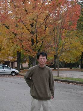
Jian-Jang Huang Assistant Professor Prof. Jian-Jang Huang received the B.S. degree in Electrical Engineering and the M.S. degree in Electrooptical Engineering from National Taiwan University in 1994 and 1996 and the Ph.D. degree in Electrical Engineering from the University of Illinois, Urbana-Champaign, in 2002. Prof. Huang had worked with WJ (Watkins Johnson) Communications in California , as a Staff Scientist from 2002 to 2004. His job function included design and characterization of high-speed electronic devices/circuits for wireless communications. He was also responsible for troubleshooting and benchmarking RF power amplifiers and mixers in the production level. He then came back to Taiwan in 2004 and stayed in Himax Tech. for a short time before joining the faculty members of the Graduate Institute of Electro-optical Engineering at National Taiwan University. |
 |
Prof. Huang currently focuses on the fabrication and characterization of whitelight LED devices for general luminance and backlit purpose. He is involved in the study of alternative semiconductor materials to realize red, green and blue light emissions. He is also interested in the device fabrication and modeling of metal oxide and organic thin film transistors for transparent and flexible circuits and displays. During his leisure, Prof. Huang likes mountain climbing, tennis, and “tee-time” (well, but golfing in US, not in Taiwan anymore). He also practices Yoga. Despite all the hobbies above, having a cup of coffee in the bookstore is probably what he enjoys most. Moreover, after getting married in 2005, he finds out that escorting his wife around the department stores in Tien-Mu area has become the priority of his weekend activities. |
|
|
|
Wing-Kit Choi Assistant Professor Born in Hong Kong, Prof. Choi received his B.Eng. degree from University of London in 1994 and his Ph.D. degree from University of Cambridge in 1998, both in Electronic and Electrical Engineering. With the award and support of a full scholarship, his Ph.D. research at Cambridge was related to high speed liquid crystal electro-optic effects & devices for use in telecommunication systems. |
|
After his Ph.D., Prof. Choi came to Taiwan with his wife (a Taiwanese whom he met in UK) and joined the new and booming TFT-LCD industry. He worked in Unipac Optoelectronics (now AUO), HsinChu Science Park as a Research and Development Engineer for about two years. At Unipac, he was responsible for the development of advanced liquid crystal technologies for TFT-LCDs. After Unipac, he joined CREOL of University of Central Florida (UCF), US as a Research Scientist. At UCF, he worked with Prof. S.T. Wu on a number of projects related to TFT-LCDs and optical communications. In both jobs (i.e. in Taiwan and US), Prof. Choi had several original invention disclosures / Patents on TFT-LCDs & liquid crystal technologies. In 2004, he returned to Taiwan and joined GIEOE of National Taiwan University (NTU) as an Assistant Professor. His current research interests at NTU include Transflective, fast-response and wide-viewing-angle TFT-LCDs. Regarding the prospect of Optoelectronics industry in Taiwan, Prof. Choi is very positive about it. In particular, he has witnessed by himself the amazing growth and developments of the TFT-LCD industry in Taiwan over the past few years. Prof. Choi believes that Taiwan, as one of most competitive countries in the world for Hi-Tech industry, has all the capability and the necessary experiences & talents for nurturing and maintaining the growth of this 21st-century “Star” industry. Prof. Choi’s main interest/hobby is music. In particular, he has quite a strong passion for listening to and playing the piano music. In recent years, Prof. Choi has also been very keen on the development of “Body, Mind & Spirit” as he has experienced some of its important benefits such as helping one to achieve a more balanced & fulfilling life.
|
|
| Professor Hao-Hsiung Lin Molecular Beam Epitaxy Laboratory Research focus: Epitaxial growth of III-V compound semiconductor alloys, nanostructures, and optoelectronic devices |
 |
The major facilities of molecular beam laboratory are two VG V-80H molecular beam epitaxy (MBE) systems, a solid source system and a gas source system, which have been devoted on the growth of III-V compound alloys and devices for over a decade. The past research works conducted in this laboratory included AlGaAs/GaAs and InAlAs/InGaAs heterojunction bipolar transistors (HBTs), 980 nm InGaAsP/InGaAs strain-compensated quantum well (QW) lasers, mid-infrared (MIR) InAs/InGaAs strained QW lasers, InAsN diluted nitride QW and lasers, InAs quantum dot (QD) and lasers, and GaAsSb/GaAs type-II QWs . The works on InAs QD and GaAsSb QW devices are still persisting. Our interest is on the feasible growth methods to manipulator the size and density of the QD for extending the emission wavelength of the lasers. For type-II QW, the band line-up engineering by introducing indium or nitrogen into GaAsSb is currently under investigation. The purposes are to understand the band structure of these alloys and to optimize the performances of optoelectronic devices through the adjustment of band gap and band offset. In additions, we also devoted to the research of 3-5 mm Sb-based MIR materials including InAsPSb quaternary and InGaAsPSb quinternary. Our target is to find suitable alloy composition for QW or QD structures for low cost and high efficient MIR light sources.
| Professor Ching-Fuh Lin Nano-semiconductor Photonic Lab Research focus: Quantum-well/quantum dot light emission components, nano-structured Si-based light emitters, fabrication and optoelectronic applications of nano-structures |
 |
Nano-meter is equal to 10-9 meter, used to measure the length of a dimension. When semiconductors or material with its size of structures as small as a few nanometers, quantum effects appear. Then their physics and optoelectronic behaviors are different from classical physics. For example, quantum wells have specific quantized energy levels, which can improve the performance of semiconductor lasers, so quantum-well lasers are popularly used in many areas now. In past years, we have put different types of quantum wells in the same device, each type of quantum well corresponding to its own emission wavelength and bandwidth. In this way, the overall bandwidth increases several times, so one single semiconductor optical amplifier is able to cover the entire optical-communication band, almost from 1300 nm to 1600 nm. Recently nano-meter research has attracted even more attractions because lots of behaviors in this scale are beyond what were expected before. In the Si semiconductors, we found that nano-structures/particles could change the recombination behaviors of electrons and holes, increasing the light emission efficiency of Si to beyond previous expectation for indirect-bandgap crystals. However, the influences of nano-meter scale could be positive or negative. In the fabrication of nano-structures or applications of nano-particles, we have to maintain the good quality of Si crystals so that the non-radiative recombination is low.
We are highly interested in the photonic applications using nano-structures. We will investigate the influences of nano-structures on optoelectronics, apply nano-structures in optoelectronic components, study new techniques for fabricating nano-structures. Hope to combine the photonics and electronics together on a single Si chip for inter-chip or on-chip optical communication.
| Professor Chee-Wee Liu Advanced Silicon Device and Process Lab Research focus: CMOS optoelectronics, CMOS image sensor, strained Si/Ge FET, SiGe/Si OEIC and PA |
|
(1). CMOS Optoelectronics:
The light emitting diodes (LEDs) and photodetectors using available CMOS technology are our focus in the field of optoelectronics. Now the LED efficiency is being improved effectively with nanotechnology enhancements such as Ge/SiC/SiGe quantum dots, surface plasmom, high-k dielectric, nanoroughness and external mechanical strain. The photodetectors are widely used in night-vision scope, video recorder, and digital camera. The germanium on insulator (GOI) phodetectors manufactured by direct wafer bonding and smart cut techniques can increase the responsivity and the speed. Although the charge coupled device (CCD) is the most important photodetector, it has a slow data record speed because the output data should be sequential read out. The first MIS Tunneling LED and MIS Tunneling photodetector are proposed by our group. The MIS structure includes ultra-thin oxide layer (only a few nm) and photocurrent can tunnel though it from metal gate to Si substrate. The MIS Tunneling photodetectors have the benefits of simplicity, fast, low cost, and easily compatible with circuits on Si substrate.
(2). Device Simulation and Modeling:
Simulation and Modeling on Si/Ge HBTs, strained Si, and Si/Ge HPTs are proposed. The Models of RF and digital circuit are also developed.
(3). Strained Si CMOS and Si/Ge HBTs:
Due to the scaling of devices, the traditional CMOS process can not satisfy the requirements of ITRS Roadmap. At present, the technique of strained Si has been widely used in the industry. Strained Si devices have a speed enhancement of 10-20% due to the high carrier mobility. The technique of package/mechanical strain is developed to optimize the design and characteristics of devices.
(4). Ge FET:
There are many papers about Ge proposed because the carrier mobility of Ge is higher than that of Si. However, the Ge-based device can not be available due to the instability of Ge oxide. We use a new structure to manufacture the first Ge FET. It not only has very low defect densities but also improves the hole mobility remarkably due to the mechanical strain.
(5). CMOS and Si/Ge HBT Design:
We focus on RF circuit design, including the power amplifier (PA) and trans-impedance amplifier (TIA). And we verify that the performance of circuit is improved by the theory of strained Si. The circuits such as ring oscillator and TIA are being optimized to use the strained Si devices. For pure bipolar, the power PA for 802.11a+b+g is being developed by using low cost SiGe HBTs. The integrated photodetectors and TIA are being developed.
(6). Rapid Thermal Process (RTP) Equipments:
In addition to the well-equipped functions such as RTA, RTO, and RTCVD, a new wafer bonding technique is developed. It not only reduces the cost but also improves the uniformity very well.
|
|
|
|