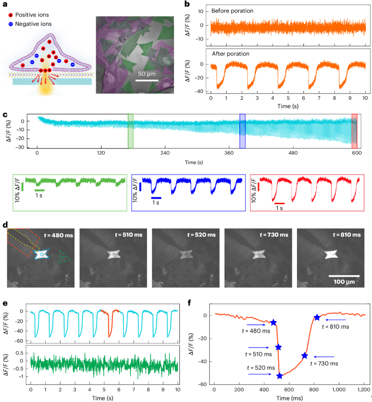
|
Ultrahigh-Definition Microarrays Using Color-Purified Conversion Technology for Micro-LED Displays
Professor Ching-Fuh Lin
Graduate Institute of Photonics and Optoelectronics, National Taiwan University
台湾大学光电所 林清富教授
Micro-light-emitting diodes (micro-LEDs), owing to their outstanding performance characteristics, are considered a leading technology for next-generation displays. However, their further development and commercialization are hindered by critical challenges, particularly those associated with mass transfer processes, which suffer from limited speed, high cost, and low production yield. To address these limitations, we propose ultrahigh-resolution color-conversion microarrays as an alternative approach for multicolor micro-LED displays. A key focus of our research is overcoming the intrinsic drawbacks of QD-based color conversion materials that usually involve toxic heavy metals (e.g., cadmium), poor environmental stability, susceptibility to moisture and oxygen, and non-uniform dispersion. Additionally, the core–shell architecture of QDs often necessitates thick conversion layers, restricting achievable light emission density and resolution.
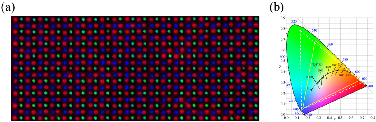
To tackle these constraints, we developed a rare-earth-free, organic–inorganic hybrid material featuring high color conversion efficiency, excellent environmental durability, and compatibility with high-resolution patterning. Leveraging well-established photolithography, we fabricated monochromatic microarrays with resolutions up to 14,115 PPI and panchromatic arrays up to 7058 PPI, with individual pixels of 1×1 µm. The patterning process is highly flexible, enabling customizable pixel layouts through mask design. To maximize color purity and light output efficiency, the hybrid microarrays are integrated with a color-purity-enhancement film based on a recycling reflection mechanism. This film selectively transmits converted red and green light while reflecting unconverted blue excitation light back into the color conversion layers for reabsorption and further conversion. Under blue light excitation, our hybrid thin films achieve high conversion efficiencies of 77.9% for green and 71.6% for red, with a thickness of only 1.5 µm. Figure 1a shows the RGB micropixel arrays fabricated on the color-purity-enhancement film. As illustrated in Figure 1b, the resulting color gamut reaches 139.12% of the DCI-P3 standard. Integration with active-matrix driver ICs is currently underway and shows promising preliminary results. Altogether, this work presents a novel and scalable pathway toward high-performance, full-color micro-LED displays.
|
|
|
Figure 1. (a) RGB micro-pixel arrays fabricated on the color-purity enhancement film under blue light illumination. (b) Color gamuts of the hybrid microarrays with the enhancement film (white area) and the DCI-P3 standard (yellow area) for comparison.
|
Highlights of Multi-Intrinsic Layer Ge PIN Photodetector Research
Professor Chee-Wee Liu
Graduate Institute of Photonics and Optoelectronics, National Taiwan University
台湾大学光电所 刘致为教授
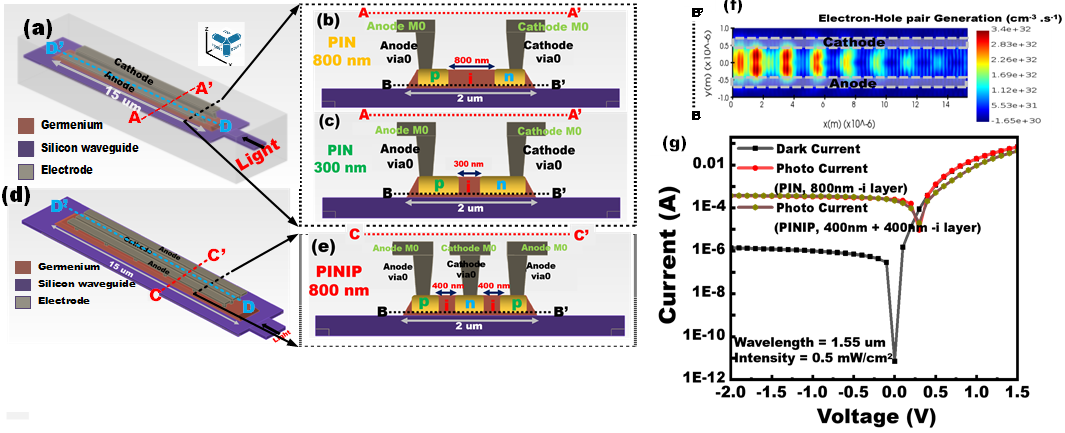
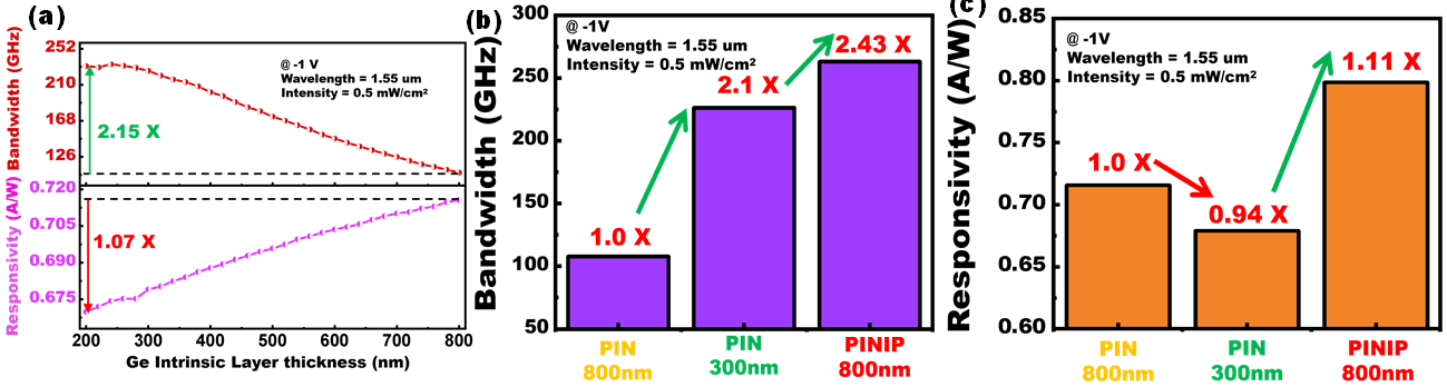
Photodetectors with bandwidths greater than 100 GHz are key components in high-speed photonics. In this work, we report on Finite-Difference Time-Domain (FDTD) and CHARGE simulations to study the optical bandwidth and the responsivity of Ge-on-Si lateral PIN photodetectors with different intrinsic layer widths (Fig. 1(a-c)) [1-2]. The FDTD solver is set with an input intensity of 0.5 mW/cm2 at a wavelength of 1550 nm under normal incidence, considering the material properties with a wavelength-dependent complex refractive index. This setup offers an electron-hole pair generation, as shown in Fig. 1(f), used in the CHARGE solver. Next, electrostatic (CHARGE) simulations are carried out, wherein material properties are defined, and physics-based models are implemented to analyze charge transport. Once these foundational steps are completed, we conduct some key simulations such as DC simulation (Fig. 1(g)) for photo-current, dark current, responsivity, transient simulation for carrier transit time, and small signal optical AC (SSAC) simulation for 3dB bandwidth, revealing device’s frequency response. The Germanium (Ge) PIN photodetector shows a trade-off between responsivity and bandwidth as the Ge intrinsic layer width decreases (Fig. 2(a)). Here we proposed PINIP photodetector design, where two PIN structures are utilized (Fig. 1(d-e)), each with a 400 nm intrinsic layer (400 nm + 400 nm), resulting in a total intrinsic layer width of 800 nm. This configuration significantly enhances the transit-time-limited bandwidth by 2.43x, reaching 263 GHz, compared to a single PIN photodetector with the same total intrinsic layer width with a stable responsivity of 0.79 A/W at -1V (Fig. 2(b-c)). [2]
|
|
|
Fig. 1. (a) 3D schematic of a Ge PIN photodetector. (b) Cross-sectional view (A-A') of the PIN photodetector with an intrinsic layer width of 800 nm, and (c) with an intrinsic layer width of 300 nm. (d) 3D schematic and (e) cross-sectional view (C-C') of a Ge PINIP photodetector, illustrating light propagation through the silicon waveguide, (f) electron-hole pair generation along B-B', as simulated using FDTD, and (g) I-V characteristics of Ge PIN and PINIP photodetectors using CHARGE. [2]
|
|
|
|
Fig. 2. (a) Analysis of the trade-off between increasing bandwidth and reducing responsivity in a Ge PIN photodetector by decreasing the intrinsic layer width, operating at -1 V. (b) Bandwidth, and (c) responsivity comparison among the PIN photodetector with 800 nm and 300 nm Ge intrinsic layer widths, and the PINIP photodetector with two 400 nm intrinsic layers. [2]
|
Reference:
[1] Avishek Das et al. in Symposium on Nano-Device Circuits and Technologies, Aug 19-21, 2024.
[2] Avishek Das et al. in IEEE Symposium on VLSI Technology, Systems and Applications, April 21-24, 2025.
|