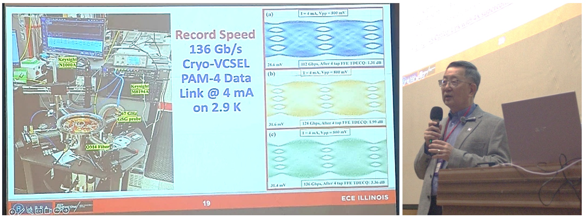
|
Fast-Response FFS LC device with multi-rubbing angle for VR applications
Professor Wing-Kit Choi
Graduate Institute of Photonics and Optoelectronics, National Taiwan University
台湾大学光电所 蔡永杰教授
We propose new fast response FFS LC devices with virtual walls by using alternating (or multi) rubbing directions, which can be generated by using photo-alignment. These new devices can offer much-enhanced response-speed compared to the conventional FFS LC device. By choosing different types of “local” LC molecular arrangements or designs (e.g. by using photo-alignment), we may be able to alter the virtual wall pitch length, and hence also alter the response speed and transmission of these fast response LC devices. These new designs can provide a new and alternative approach to generating virtual walls by “locally” varying the rubbing angle using photo-alignment. These devices are attractive for VR applications where high speed operation of liquid crystal devices is required.
|

|
|
Fig. 1. Top view of our new fast-response FFS LC mode with alternating rubbing angles.
|
|

|
|
Fig. 2. Compared to conventional FFS LC cell (blue), our new designs of FFS with alternating rubbing angles show a shortening of the response time (fall time) from about 14ms to about 5ms (~3X improvement) for design B (gray) whereas a further shortening of response time (fall time) from about 14ms to about 2ms (~7X improvement) for design A (orange).
|
Reference:
Shi-Rui Chen and Wing-Kit Choi, “Fast-Response FFS LC Device with Multi-rubbing Angle for VR Applications,” SID technical digest, vol: 55, issue 1, p.2075-2077, 2024
Strong Coupling between All-dielectric Metasurfaces and Epsilon-near-zero Modes for Broadband Third Harmonic Generation
Professor Hui-Hsin Hsiao
Graduate Institute of Photonics and Optoelectronics, National Taiwan University
台湾大学光电所 萧惠心教授
Third-harmonic generation (THG) is a nonlinear optical process in which three photons at the excitation frequency interact within a nonlinear medium to generate a single photon at three times the excitation frequency. This process has significant applications in microscopy, laser technology, and spectroscopy.
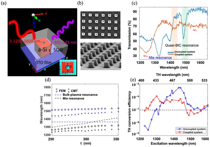
Here, we propose a nonlinear hybrid metasurface composed of amorphous silicon nanocubes on an ultrathin Indium Tin Oxide (ITO) film to explore the coupling effect among Mie resonance, quasi-bound states in the continuum (QBICs), and the epsilon-near-zero (ENZ) guided mode. Through near-field analysis and coupled mode theory (CMT), we demonstrate that Mie-ENZ coupling is significantly more efficient than QBIC-ENZ coupling, aligning with the critical coupling condition. This strong coupling effect is accompanied by a large Rabi splitting energy of 190 meV. In experiment, our nonlinear hybrid metasurface exhibits an ultra-broadband THG enhancement, achieving a measured conversion efficiency exceeding 10-7 within the spectral range of 1230-1600 nm. Notably, a more than ten-fold TH enhancement is observed in the blue light region (410-450 nm) when comparing the coupled and uncoupled systems. These results highlight the potential of hybrid metasurfaces as a platform for broadband light sources, wide-range dielectric spectroscopy, and high-resolution imaging with extended spectral coverage.
|
|
|
Fig. (a) Schematic view of the nonlinear hybrid metasurfaces. (b) SEM images of the fabricated samples. (c) Measured linear optical transmission spectrum for the uncoupled (blue curve) and coupled (red curve) systems. (d) Resonant wavelengths of two hybridized resonances as a function of the nanocube height t. (e) Measured TH conversion efficiency spectra for the uncoupled (blue dots) and coupled (red dots) systems.
|
300 GHz Low-Cost PCB Vivaldi Antenna Array and Transition Structure to WR-3 Waveguide
Professor Yu-Hsiang Cheng
Graduate Institute of Photonics and Optoelectronics, National Taiwan University
台湾大学光电所 郑宇翔教授
We design a four-element Vivaldi antenna array, a 1-to-4 power divider for signal distribution, and a transition structure to a WR-3 waveguide. The power divider utilizes substrate integrated waveguides, while the transition to the rectangular waveguide is achieved through a coupled patch antenna structure. The entire antenna array and transition structure are printed on a single layer of circuit board substrate, with linewidths exceeding 0.125 mm to ensure cost-effective manufacturing. Simulation results of the array antenna with the transition structure show a peak realized gain of 13.6 dBi, with gain variation within the operating frequency band of 272-311 GHz remaining under 0.4 dB, making it suitable for operation in IEEE 802.15.3d channel 67. The measured gain pattern and reflection coefficient of both the individual antenna elements and the array antenna align closely with the simulation results.
|

|
|
Fig. The photo of the fabricated Vivadi antenna array. The simulated and measured reflection coefficient and radiation patterns in the E plane and H plane.
|
Reference:
Zhao-Fa Chen, Zhao-Hong Tu, Chih-Han Lin, and Yu-Hsiang Cheng, “300 GHz PCB Vivaldi Antenna Array and Transition Structure to WR-3 Waveguide,” IEEE Access 12, 92169 (2024)
|