|
Broadband InSe/MoS2 Type-II Heterojunction Photodetector with Gate-Tunable Polarity
Professor Yuh-Renn Wu
Graduate Institute of Photonics and Optoelectronics, National Taiwan University
台湾大学光电所 吴育任教授
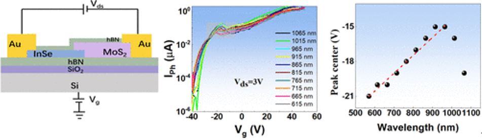
The development of two-dimensional (2D) van der Waals heterojunctions has opened new possibilities for advanced optoelectronic devices, particularly in broadband photodetection. In this work, we demonstrate a broadband InSe/MoS2 type-II heterojunction photodetector with gate-tunable polarity, enabling a near-linear wavelength-dependent photocurrent peak. The vertically stacked InSe/MoS2 heterojunction exhibits broadband detection from 400 nm to 1064 nm, with a high responsivity of 10,200 A/W at 532 nm and −1430 A/W at 1064 nm, as well as a maximum photodetectivity of 3 × 1013 cm Hz-1/2 W-1. The device displays both positive and negative photoconductivity, depending on incident light energy, and a gate-tunable polarity transition at Vg = −20 V, which induces a photocurrent peak shifting nearly linearly with wavelength.
|
|
|
Fig. 1.
|
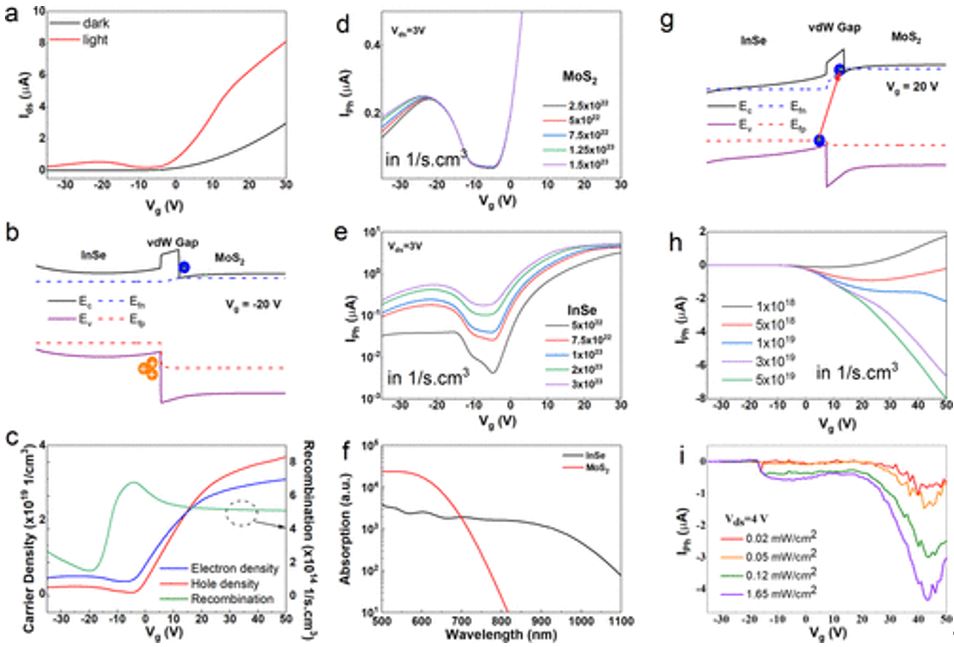
To gain deeper insight into the underlying mechanisms, we performed Poisson and drift-diffusion simulations to model the charge carrier dynamics within the InSe/MoS2 heterojunction. As shown in Figure 2a, our simulations successfully reproduce the experimentally observed gate-tunable photocurrent peak. The calculated potential profile (Figure 2b) confirms the presence of a type-II band alignment, where electrons and holes accumulate at the heterojunction interface. Furthermore, the simulation results (Figure 2c) reveal that the photocurrent peak is governed by the balance between electron accumulation in MoS2 and hole accumulation in InSe, which shifts with incident wavelength and power density. Notably, our simulations also explain the negative photoresponse under infrared illumination, attributed to trap-assisted interlayer charge transfer at the heterojunction interface (Figure 2h).
These findings demonstrate the potential of gate-tunable 2D heterojunctions for high-performance optoelectronic applications, such as tunable spectrometers, reconfigurable photodetectors, and integrated photonic circuits. The ability to control the device polarity and photoresponse via gate voltage provides new opportunities for designing multifunctional optoelectronic devices.
|
|
|
Fig. 2. (a) Simulated Ids–Vg characteristic curves in darkness and under light illumination at Vds = 3 V. (b) Calculated potential profile along the vertical direction at the overlap region at Vg = −20 V under illumination, where Ec, Ev, Efn, Efp are the conduction band minimum, valence band maximum, quasi-Fermi level for electron, and quasi-Fermi level for hole, respectively. (c) Calculated carrier density and nonradiative recombination rate at interface. (d) IPh–Vg curves were simulated with a variety of generation rates for MoS2 while keeping the same generation rates for InSe (1 × 10²³ 1/scm3). (e) IPh–Vg curves were simulated with a variety of generation rates for InSe while keeping the same generation for the MoS2 layer (1 × 10²² 1/scm3). (f) Calculated absorption coefficient for InSe and MoS2 layers as a function of wavelength. (g) Calculated potential profile along the vertical direction at the overlap region at Vg = 20 V. (h) Simulated IPh–Vg with different densities of electron trapping at the interface. (i) IPh–Vg characteristic curve under 1064 nm laser illumination at Vds = 4 V.
|
Reference:
Wenying Zhang, Kuan-Hao Chiao, Hsin-Wen Huang, Mohamed Abid, Cormac Ó Coileáin, Kuan-Ming Hung, Ching-Ray Chang, Yuh-Renn Wu,* and Han-Chun Wu*, "Broadband InSe/MoS2 Type-II Heterojunction Photodetector with Gate-Tunable Polarity Induced Near-Linear Wavelength-Dependent Photocurrent Peak," ACS Applied Materials & Interfaces, 2025, 17, 12941−12951. DOI: 10.1021/acsami.4c22132.
Ultra-high thermal sensors based on quantum-well heterojunction bipolar transistors
Professor Chao-Hsin Wu
Graduate Institute of Photonics and Optoelectronics, National Taiwan University
台湾大学光电所 吴肇欣教授
We are thrilled to share a groundbreaking achievement in the field of optoelectronics and high-speed device technology: the successful design and fabrication of the world’s first Darlington transistor utilizing cascaded Light-Emitting Transistors (LETs) with ultra-high thermal sensitivity.
|
|
|
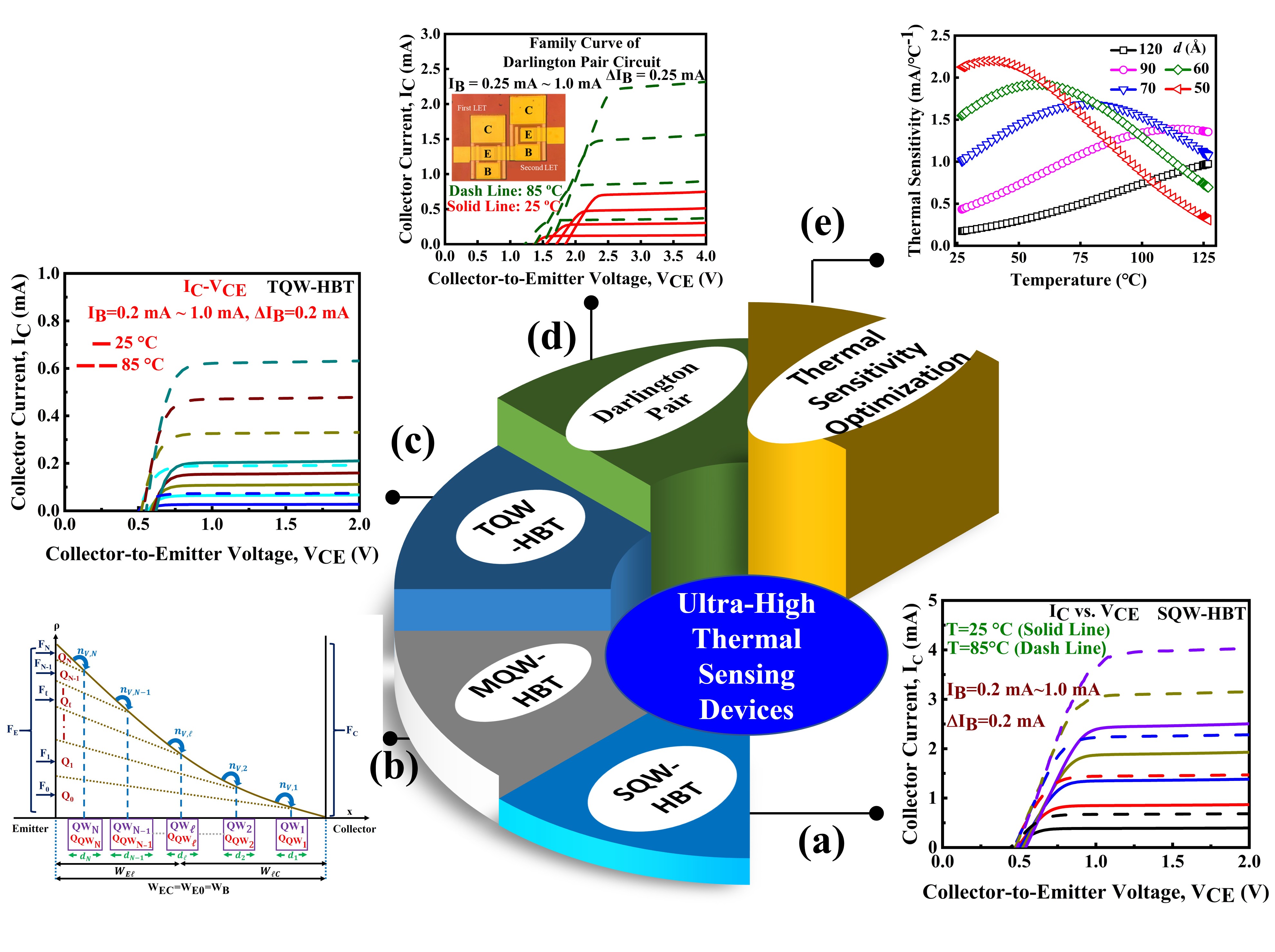
Fig. 1. (a): IC vs. VCE of n-p-n InGaP/GaAs SQW-HBT at different substrate temperatures [1]. (b) Schematic of minority carrier distribution (ρ) in the base region of an MQW-HBT [2]. (c) IC vs. VCE of n-p-n TQW-HBT at varied IB (0.2 mA to 1 mA), measured at Text = 25 ºC (solid line) and Text = 85ºC (dashed line) [3]. (d) IC vs. VCE at different IB (0.25 mA to 1 mA) at various substrate temperatures. The inset shows the Darlington transistor device contacts and applied bias configuration, with 500 Ω resistance (R) connecting C2 to VDD [4]. (e) Collector current derivation as a function of temperature for varying QW-widths (50 Å, 60 Å, 70 Å, 90 Å, and 120 Å) [5].
|
Our research demonstrated that the single-quantum-well heterojunction bipolar transistor (SQW-HBT) exhibits a remarkable 73.23% increase in collector current (IC) as the temperature rises from 25 ºC
to 85 ºC
under a base current (IB) of 0.2 mA and a collector-to-emitter voltage (VCE) of 2 V, a behavior contrasting the typical thermal response of conventional HBTs, as shown in Fig. 1(a) [1]. Building on these findings, we developed a modified charge-control model for multiple-quantum-well (MQW)-based HBTs, optimizing QW parameters such as number, size, width, position, and barrier width to enhance the efficiency of LETs for thermal sensor applications, as shown in Fig. 1(b) [2]. Using this model, we engineered triple-quantum-well (TQW)-HBTs that achieved a 200% increase in IC as temperature rose from 25 ºC
to 85 ºC at IB of 1 mA and VCE of 2 V, as shown in Fig. 1(c), marking a significant step toward high-temperature applications [3].
Leveraging these advancements, we designed a novel Darlington transistor by cascading two LETs. The LET alone demonstrated a 153% increase in IC under temperature changes from 25 ºC
to 85 ºC
at IB of 1 mA and VCE of 4 V, while the Darlington transistor surpassed this performance, achieving a 210% increase in IC under similar conditions, as shown in Fig. 1(d). Notably, the current sensitivity of LETs reached 8.53 μA/ºC, and the Darlington transistor achieved an exceptional 26.2 μA/ºC. Additionally, the Darlington transistor reported a voltage sensitivity of 9.12 mV/ºC, significantly surpassing the performance of conventional thermal sensors [4]. Despite these achievements, challenges remain in achieving a highly linear voltage-to-temperature response due to nonlinear electron escape from the QW. To address these challenges, we proposed a QW size-dependent optimization model, achieving an optimal balance between thermal sensitivity and linearity for specific temperature ranges [5]. For instance, a QW width of 90 Å exhibited a thermal sensitivity of 1.34 mA/ºC
and a linearity fitting parameter (B) of 0.67748 within a temperature range of 25 ºC
to 100 ºC, as shown in Fig. 1(e).
Our team is committed to further modifying LET-based technologies to unlock their full potential as front-end components in smart thermal sensing applications. By optimizing QW structures, we aim to enhance linearity and sensitivity, paving the way for next-generation thermal sensor technologies with unprecedented performance. These achievements represent a significant leap forward in thermal-sensitive optoelectronic devices and hold immense promise for applications in smart sensing and beyond. We thank our collaborators and supporters for their contributions to this groundbreaking research.
Reference:
[1] M. Kumar, S.-J. Hsu, S.-Y. Ho, S.-W. Chang, and C.-H. Wu, “Current gain enhancement of heterojunction bipolar light-emitting transistor using staircase InGaAs quantum well,” IEEE Trans. Electron Devices, vol. 70, no. 10, pp. 5177-5183, Oct, 2023, doi:10.1109/TED.2023.3305355.
[2] M. Kumar, L.-C. Hsueh, S.-W. Cheng, S.-W. Chang, and C.-H. Wu, “Analytical modeling of current gain in multiple-quantum-well heterojunction bipolar light-emitting transistors,” IEEE Trans. Electron Devices, vol. 71, no. 1, pp. 343-349, Jan 2024, doi:10.1109/TED.2023.3289930.
[3] M. Kumar, S.-Y. Ho, S.-J. Hsu, P.-C. Li, S.-W. Chang, and C.-H. Wu, “Current gain enhancement at high-temperature operation of triple-quantum-well heterojunction bipolar light-emitting transistor for smart thermal sensor application,” IEEE Trans. Electron Devices, vol. 71, no.1, pp. 896-903, Jan. 2024, doi: 10.1109/TED.2023.3339084.
[4] M. Kumar, K.-Y. Hsueh, S.-J. Hsu, and C.-H. Wu, “Design and fabrication of novel Darlington transistor using light-emitting transistors for smart thermal sensor technology,” IEEE Electron Device Letters, vol. 45, no. 7, pp. 1365-1368, July, 2024, doi:10.1109/LED.2024.3401084.
[5] M. Kumar, S.-W. Chang, and C.-H. Wu, “Investigation of thermal sensitivity and linearity of quantum well-based heterojunction bipolar transistor,” IEEE Transactions on Electron Devices, Early Access, Nov 2024, doi: 10.1109/TED.2024.3492153.
|