|
Blue triplet-triplet fusion organic light-emitting diode with bi-layer emitting layer
Professor Jiun-Haw Lee
Graduate Institute of Photonics and Optoelectronics, National Taiwan University
台湾大学光电所 李君浩教授
A blue organic light-emitting diode (OLED) based on triplet-triplet fusion (TTF) was demonstrated consisting of bi-layer emitting layer (EML) structure, which were 1-(2,5-dimethyl-4-(1-pyrenyl)phenyl)pyrene (DMPPP) and carbazole-substituted anthracene (CbzAn) which acted as triplet tank layer (TTL) and triplet-triplet fusion (TTF) layer, respectively. 5% of 7,7,13,13-tetramethyl-N5,N5,N11,N11-tetraphenyl-7,13-dihydrobenzo-[g]indeno[1,2-b]fluorene-5,11-diamine (DPaNIF) was incorporated inside TTL and TTF layer as dopants. Carriers recombined at the TTL which formed 25% singlets and 75% triplets. Singlet emission happened in TTL, while triplets transferred the energy to TTF layer undergoing upconversion process followed by light emission. External quantum efficiency of this blue OLED achieved remarkably 11.12%.
Reference:
Kai-Hong Hsieh et al., Adv. Photonics Res. 2024, 2300344.
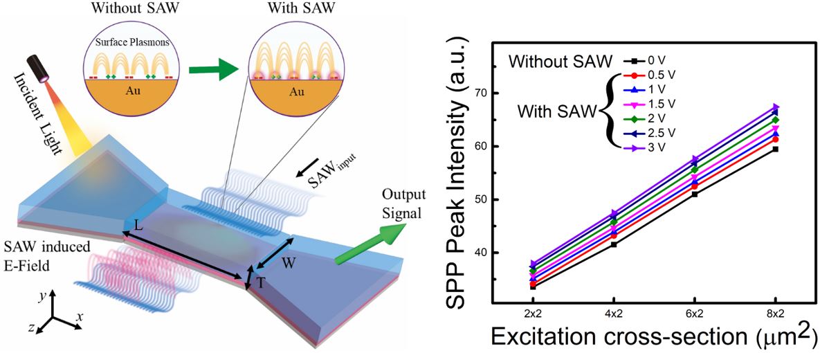
Surface Acoustic Wave Actuated Plasmonic Signal Amplification in a Plasmonic Waveguide
Professor Jian-Jang Huang's Laboratory
Graduate Institute of Photonics and Optoelectronics, National Taiwan University
台湾大学光电所 黄建璋教授
Enhancement of nanoscale confinement in the subwavelength waveguide is a concern for advancing future photonic interconnects. Rigorous innovation of plasmonic waveguide-based structure is crucial in designing a reliable on-chip optical waveguide beyond the diffraction limit. Despite several structural modifications and architectural improvements, the plasmonic waveguide technology is far from reaching its maximum potential for mass-scale applications due to persistence issues such as insufficient confined energy and short propagation length. This work proposes a new method to amplify the propagating plasmons through an external on-chip surface acoustic signal. The gold-silicon dioxide (Au-SiO2) interface, over Lithium Niobate (LN) substrate, is used to excite propagating surface plasmons. The voltage-varying surface acoustic wave (SAW) can tune the plasmonic confinement to a desired signal energy level, enhancing and modulating the plasmonic intensity. From our experimental results, we can increase the plasmonic intensity gain of 1.08 dB by providing an external excitation in the form of SAW at a peak-to-peak potential swing of 3 V, utilizing a single chip.
|
|
|