|
Simple Architecture for Highly Collimated Backlight
Professor Chung-Chih Wu
Graduate Institute of Photonics and Optoelectronics, National Taiwan University
台湾大学光电所 吴忠帜教授
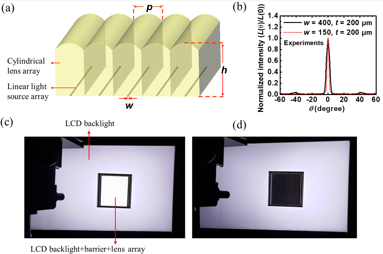
Highly collimated and directional backlights are essential for realizing advanced display technologies such as autostereoscopic 3D displays. Previously reported collimated backlights, either edge-lit or direct-lit, in general still suffer unsatisfactory form factors, directivity, uniformity, or crosstalk etc. In our study, we devise a simple stacking architecture for the highly collimated and uniform backlights, by combining linear light source arrays and carefully designed cylindrical lens arrays. Experiments were conducted to validate the design and simulation, using the conventional edge-lit backlight or the direct-lit mini-LED (mLED) arrays as light sources, the barrier sheets, and cylindrical lens arrays fabricated by molding. Highly collimated backlights with small angular divergence of ±1.45°~±2.61°, decent uniformity of 93-96%, and minimal larger-angle sidelobes in emission patterns were achieved with controlled divergence of the light source and optimization of lens designs. Such an architecture provides a convenient way to convert available backlight sources into a highly collimated backlight, and the use of optically reflective barrier also helps recycle light energy and enhance the luminance, providing a facile approach for display technologies requiring highly collimated backlights.
|

|
|
Fig. 1. (a) The schematic architecture of the highly collimated backlight. (b) Measured far-field emission patterns of the collimated backlight. (c)-(d) Light-up photos of the conventional LCD BLU stacked with the barrier and the cylindrical lens array (center area), taken along (c) the normal direction (0°) and (d) the 5° tilting angle.
|
|