|
Noise Reduction Through Square Aperture Array in Integral Imaging-based 3D Light-Field Display
Professor Hoang-Yan Lin
Graduate Institute of Photonics and Optoelectronics, National Taiwan University
台湾大学光电所 林晃岩教授
The integral-imaging based 3D light field display can restore its light-field information, reconstruct different images in different depth planes, and realize the floating projection effect. In the metaverse, AR/VR wearable devices, HUD for smart cockpits, medical care, entertainment, art performance and other scenarios, naked-eye 3D display is one of the most crucial requirements for the coming future.
We have created 3D floating images with an integral imaging-based 3D light field display. However, noise is an annoying problem after restoring information in 3D light field displays. In this study, we proposed a square aperture array to be added to the original light field display to solve the noise problem and find out that an aperture array can effectively decrease the noise. Also, the light intensity will be decreased a lot for the circle aperture array case but will not be decreased for our square aperture array design. Finally, we created naked-eye 3D images with very little noise and also without light intensity sacrifice.
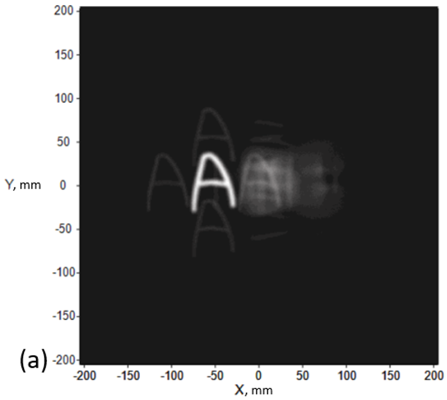
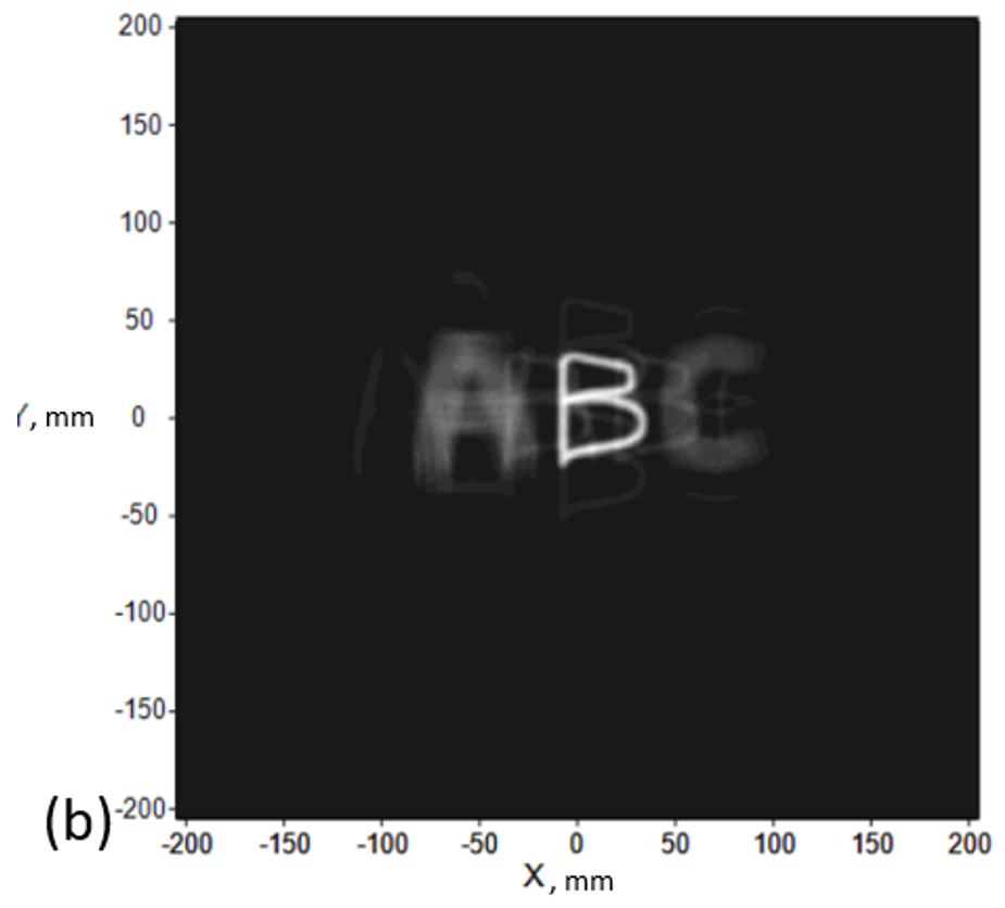
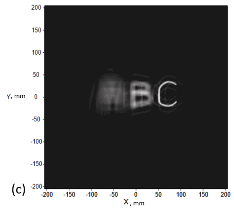
Firstly, we show a light-emitting angle = 90 degrees for the sample, we will create a picture at different depths (z) as shown in Fig. 1. Looking closely at Figs. 1 (a)(b)(c), we can find out that there are 4 dim letters A around the bright letter A and the same situation in letters B and C. We regard those dim letters as noise and it is produced by a light ray that does not obey the principle of CGEI.
|
|
|
|
|
Fig. 1 Images in different depths (z) (a) A at z = 200mm (b) B at z = 105.37 mm (c) C at z = 48 mm.
|
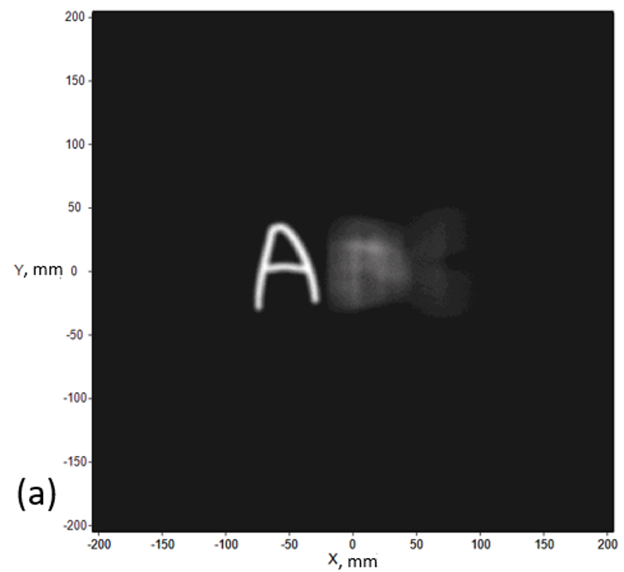
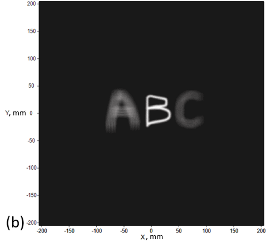
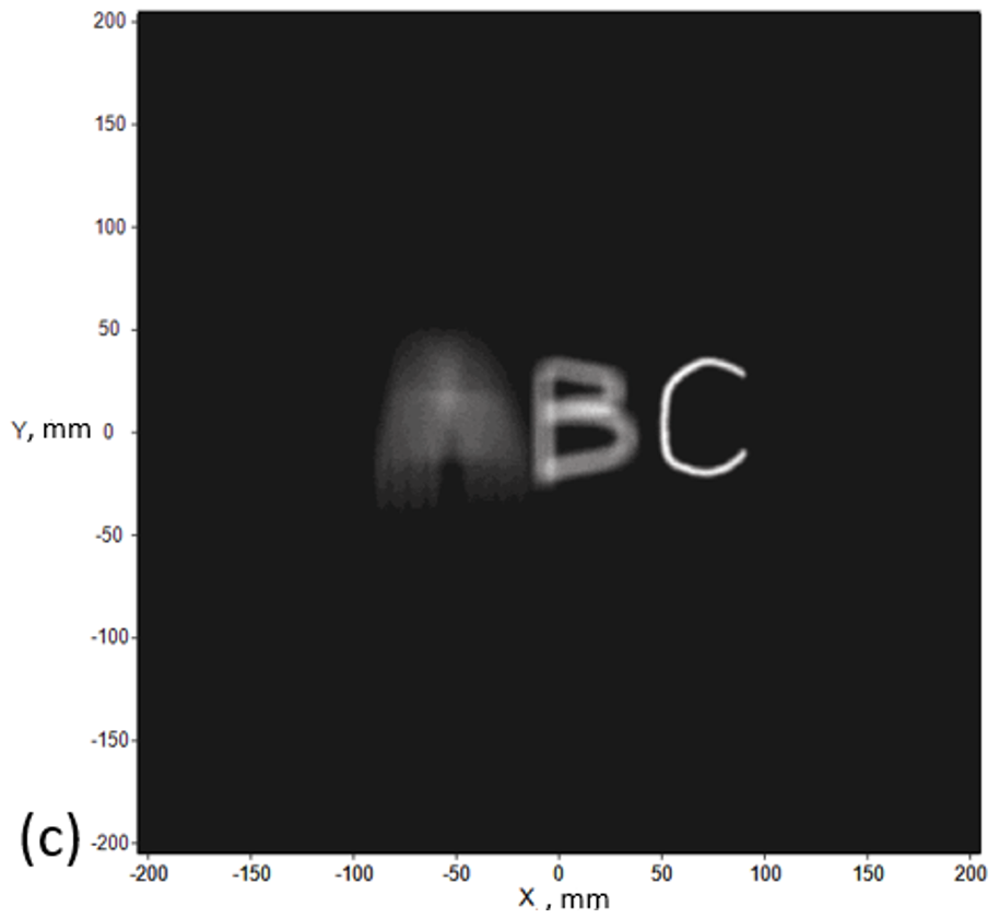
After knowing the best position of the aperture array, we have shown the restored image in different depths (z) in Fig. 2 when aperture array X=7 mm. We set parameter X for the distance between the aperture array and the display panel. We can discover that there isn’t any dim letter next to the bright letter, which means that we successfully eliminate the noise!
|
|
|
|
|
Fig. 2 Image in different depths with aperture array (a) A at z = 200mm (b) B at z = 105.37 mm (c) C at z = 48 mm.
|
Reference:
Chia-Yuan Chang and Hoang-Yan Lin, Noise Reduction Through Square Aperture Array in Integral Imaging-based 3D Light-Field Display, SID Display Week 2023.
Photonic Mixing Sub-THz Carrier for Wireless Data Link with Single-Chip Dual-Wavelength DFBLD
Professor Gong-Ru Lin
Graduate Institute of Photonics and Optoelectronics, National Taiwan University
台湾大学光电所 林恭如教授
Sub-THz wireless communication technology has emerged as a promising candidate to extend the carrier frequency toward previously unexplored bands to enable the ultra-wide-band short-range data link beyond 6G. The optical heterodyned generation of millimeter-wave wireless carriers via discrete laser sources is intriguing in view of the currently available technologies for carrier synthesis because of its flexibility on frequency tunability. However, finite modal linewidth and residual wavelength drift are two main concerns that raise the noise background to degrade the signal-to-noise ratio of the data encoded onto the heterodyned carrier. Maintaining the difference and stability of wavelength and phase between two independent lasers usually relies on additional controlling and feedback schemes such as a phase-locked loop. This inevitably induces systematic complexity and alternative solution needs to be considered for simplification. In this work, a dual-mode distributed feedback laser diode (DFBLD) is demonstrated as a monolithic wireless sub-THz carrier synthesizer with absolute wavelength (frequency) differentiation and phase synchronization between two lasing longitudinal modes. By directly encoding the DFBLD with QAM-OFDM data format, the wireless data link can be performed via such a compact and simplified sub-THz wireless transmitter.
|

|
The dual-mode-lasing DFBLD is designed by slightly tilting the DFB mirror structure by an angle
f
to the surface normal of the output end-face at one side of the resonant cavity, which enables the concurrent lasing of both longitudinal modes inside the DFBLD cavity. Such a design combined with a short cavity results in a mode spacing of 2-3 nm to cause a frequency difference tunable from 320 to 330 GHz. The dual-mode-lasing DFBLD exhibits two distinct longitudinal modes centered at 1545-1546 nm and 1547-1548 nm, respectively. The back-to-back sub-THz wireless link is demonstrated by transmitting the NRZ-OOK data stream at 5 GBaud, revealing the quality factor and bit-error ratio of nearly 4 and 5e-5, respectively. By amplifying the 16-QAM DMT data amplitude, the received constellation plot of the down-converted baseband DMT data shows a blurred spot with an increased EVM. The signal-to-noise ratio remains above 15 dB over 95% of the encoding bandwidth, providing a BER of 2.3x10⁻³ of the broadened 16-QAM formats at allowable data rates of 12 Gbit/s. The fully integrated dual-mode-lasing DFBLD chip can serve as a novel compact sub-THz transmitter as compared to those using individual laser sources and external data modulators.
本文为与台湾大学电机系郑宇翔教授合作之成果。
Reference:
1. C.-Y. Lin, Y.-C. Chi, C.-T. Tsai, H.-Y. Wang, and G.-R. Lin, “39-GHz millimeter-wave carrier generation in dual-mode colorless laser diode for OFDM-MMWoF transmission,” IEEE J. Sel. Top. Quantum Electron., vol. 21, pp. 609-618, Nov.-Dec. 2015
2. C.-T. Tsai, C.-H. Lin, C.-T. Lin, Y.-C. Chi, and G.-R. Lin, “60-GHz millimeter-wave over fiber with directly modulated dual-mode laser diode,” Sci. Rep. vol. 6, no. 27919, Jun. 2016.
|