|
Research highlights of Nanosheet/Nanowire GeSi
Professor Chee-Wee Liu
Graduate Institute of Photonics and Optoelectronics, National Taiwan University
臺灣大學光電所 劉致為教授
Nanosheet/Nanowire gate-all-around field effect transistors (GAAFETs) are used to replace FinFETs due to their good electrostatics and short channel control. Moreover, to enhance the drive current and to improve overall transistor density, channel stacking is done at the same footprint. In alignment with this trajectory, our research group has also contributed significantly by increasing the number of stacked channels. Specifically, we have successfully showcased the functionality of 16 stacked Ge0.95Si0.05 nanowires (Figure 1(a)), achieving a groundbreaking drive current of 9400μA/μm per footprint at VOV=VDS=0.5V [1]. Moreover, to further enhance transistor performance, we have implemented a novel two-step wet etching process, leading to the demonstration of 12 stacked Ge0.95Si0.05 nanowires (Figure 1(b)) without parasitic channels [1]. This resulted in minimized transistor leakage and subthreshold swing. We have also achieved the record drive current i.e. 9200μA/μm per footprint and 360μA per stack, respectively, at VOV=VDS=0.5V for 8 stacked Ge0.95Si0.05 nanosheets (Figure 1(c)) (WCH=120nm) with extremely
high-k
Hf0.2Zr0.8O2 [2]. Furthermore, our group stands the pioneer in showcasing the first stacked Ge0.98Si0.02 Nanosheet FeFET (Figure 2 (a, b) ) at the record low write voltage of 2V and endurance > 1E11 cycles [3].
|

|
|
Figure 1 (a) 16 stacked Ge0.95Si0.05 nanowires [1]. (b) 12 stacked Ge0.95Si0.05 nanowires without parasitic channels [1]. (c) 8 stacked Ge0.95Si0.05 nanosheets [2] (©2023 JSAP).
|
|

|
|
Figure 2 (a, b) 2 stacked Ge0.98Si0.02 NS GAA n-FeFETs [3] (©2023 JSAP).
|
Reference:
[1] Yu-Rui Chen et al. Communications Engineering, 2, 77, pp. 1-9, 2023.
[2] Yi-Chun Liu et al. in IEEE Symposium on VLSI Technology and Circuits JUNE 11-16, 2023.
[3] Yu-Rui Chen et al. in IEEE Symposium on VLSI Technology and Circuits JUNE 11-16, 2023.
Structured NIR and Yellow-Orange Light Generation from
c(2) Nonlinear Photonic Crystals
Professor Lung-Han Peng
Graduate Institute of Photonics and Optoelectronics, National Taiwan University
臺灣大學光電所 彭隆瀚教授
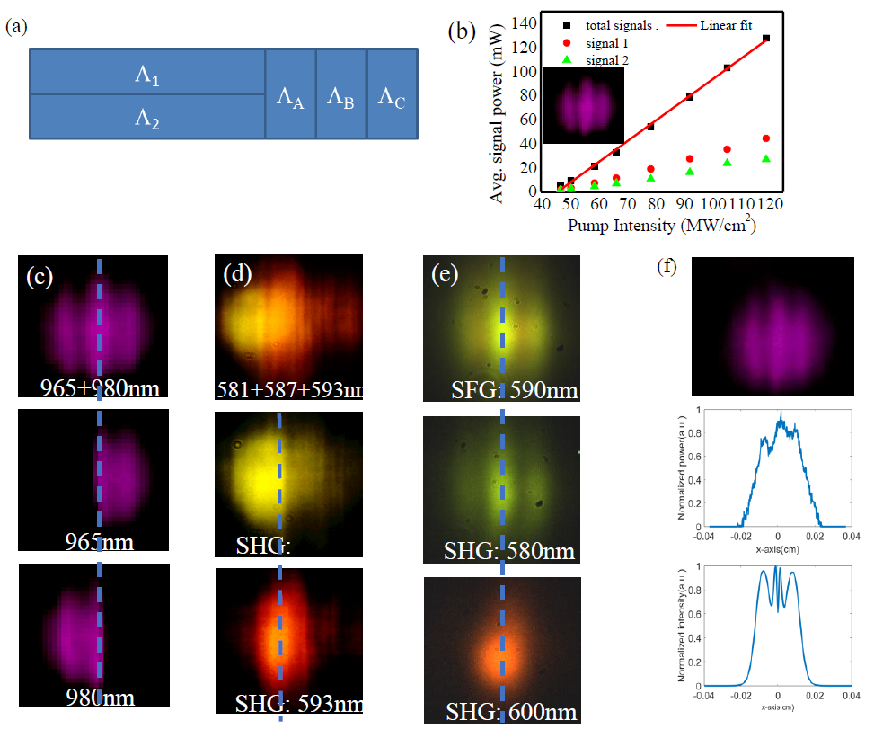
Structured beams have been useful to some research fields, like quantum communication, super-resolution microscopy, and particle manipulation. Conventional ways of structured beams generation require liquid-crystal spatial light modulator (SLM) or q-plate which will complicate the whole optical layout thus limiting their application. In this study, we propose a nonlinear mode converter which will not only produce structured light, but also generate new frequency of light. Fig. 1(a) shows our structured NIR and visible mode converter design, in the parallel bi-grating part, the generated signal and idler will become structured. Then, these structured idler waves will be up-converted into visible light via second harmonic and sum frequency generation, and naturally, the up-converted visible light will also be structured. Our design shows another way to the structured beams generation which will be applicable to the UV band.
|

|
|
Fig. 1 (a) Design of nonlinear mode converter, where Λ1= 7.66 mm, Λ2= 7.68 mm, ΛA= 9.915 mm, ΛB= 10.188 mm and ΛC= 10.468 mm. (b) the output power of dual signal waves with respect to the pump intensity. Inset: the transverse mode of structured dual signal waves. (c) the transverse modes of dual signal, signal 1 and signal 2. (d) the transverse mode of the up-converted visible light (e) by adding additional grating, the structure mode of visible will become clear. (f) from top to bottom are the transverse mode, experimental intensity profile and numerical mode simulation of the dual signal waves.
|
|