|
Low-Cost 3D-Printed Large-Area 1-DOF Scanners
Professor Jui-che Tsai
Graduate Institute of Photonics and Optoelectronics, National Taiwan University
台湾大学光电所 蔡睿哲教授
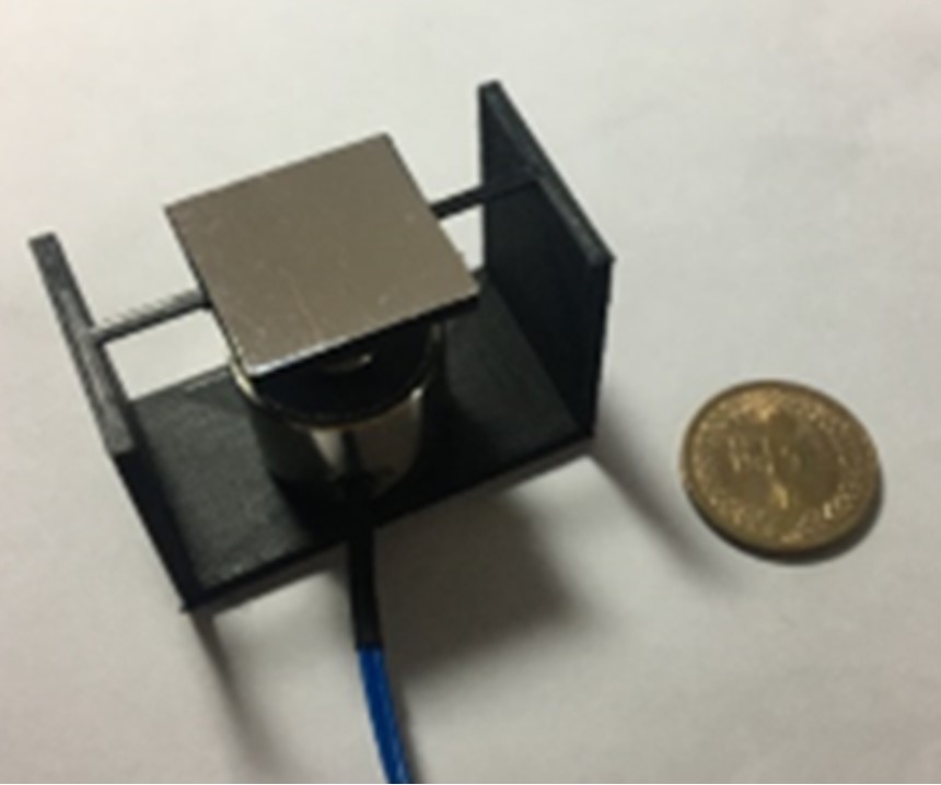
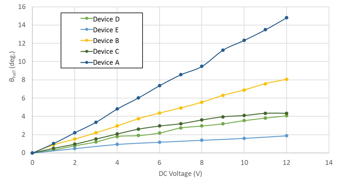
We have developed 3D-printed 1-DOF (one torsional axis; 1 degree of freedom) optical scanners with large mirror areas (up to 20 × 20 mm2). Each device consists of an aluminum-coated square silicon substrate serving as the mirror, two miniature permanent magnets, an electromagnet, and a 3D-printed structure including the mirror frame, torsion springs, and base. One device can reach a static half optical deflection angle of 14.8 deg. at 12 VDC; this particular device exhibits a mechanical resonance frequency of 84 Hz. These scanners can be a potential, low-cost alternative to the expensive conventional galvanometer scanners.
|
(a)
|
(b)
|
|
|
|
|
Fig. 1. (a) Device with a 20 × 20 mm2 mirror area (Device A). (b) Static characteristics: optical half angle θhalf vs. dc voltage for different devices.
|
Shen, C.-K.; Huang, Y.-N.; Liu, G.-Y.; Tsui, W.-A.; Cheng, Y.-W.; Yeh, P.-H.; Tsai, J.-c.*, “Low-Cost 3D-Printed Electromagnetically Driven Large-Area 1-DOF Optical Scanners,” Photonics, vol. 9, no.7, 484, Jul. 2022.
Carrier localization in III-nitride versus conventional III-V semiconductors: A study on the effects of alloy disorder using landscape theory and the Schrödinger equation
Professor Yuh-Renn Wu's Laboratory
Graduate Institute of Photonics and Optoelectronics, National Taiwan University
台湾大学光电所 吴育任教授
Semiconductor devices often necessitate the practice of band-gap engineering, a process that involves the utilization of alloys and the fine-tuning of their composition to achieve the desired electrical or optical characteristics. While deviations in composition are typically considered minor perturbations in conventional III-V semiconductors, the impact of alloy disorder is significantly more pronounced in III-nitrides. This study aims to compare the influence of alloy disorder on carrier localization, focusing on various III-V semiconductors, particularly with regard to holes, where localization effects are more pronounced due to their greater effective mass.
To conduct this investigation, we employ three-dimensional computational methods for III-V alloys featuring natural (random) compositional fluctuations. Given the intricacy of the problem, our computations are based on a simplified Hamiltonian within the envelope wave-function approximation, focusing on a single heavy-hole valence band. We explore the impact of compositional fluctuations on carrier localization using two distinct approaches.
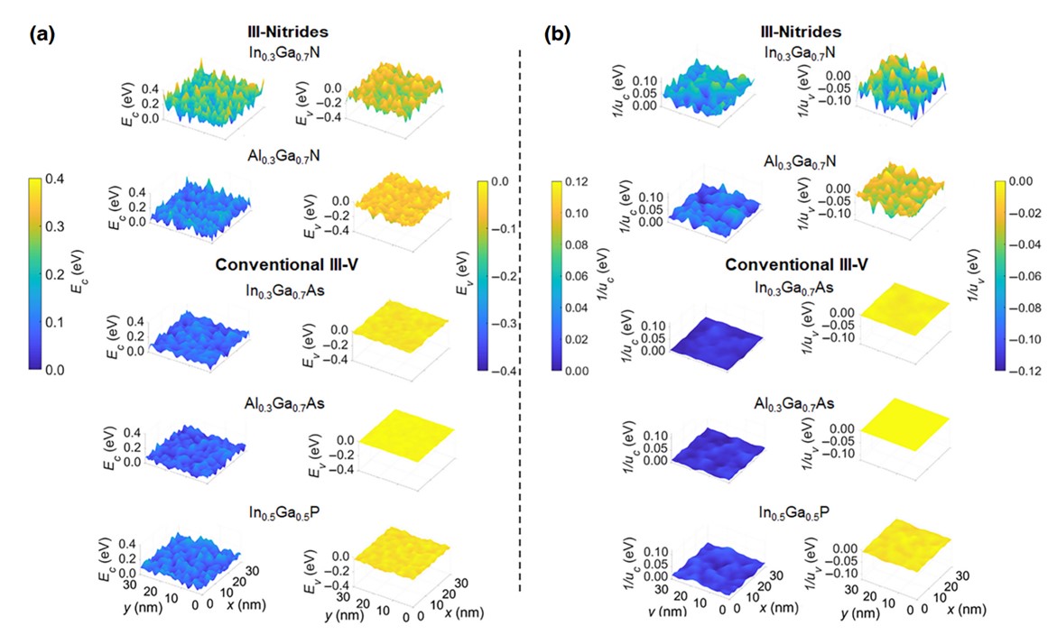
The first approach leverages the localization landscape theory, allowing us to solve the localization landscape equations and derive the effective potentials that act upon carriers. These potentials serve as confining forces, predicting the spatial regions where carriers are most likely to be localized. This enables a comparative analysis of the effects of alloy fluctuations between conventional III-V and III-nitride semiconductors. Notably, we observe that the effective potential in III-nitride semiconductors exhibits considerably larger fluctuations compared to other III-V semiconductors, potentially indicating a higher degree of carrier localization in nitrides, particularly for holes.
To validate this observation, we employ the second method, solving Schrödinger's equation to determine the electron and hole wave functions. Our findings reveal that in InxGa1−xN, electron wave functions tend to be delocalized, even in the ground state, while low-energy hole states exhibit localization. This contrasts with the behavior of holes in the common alloy InxGa1−xAs, where they are consistently found to be delocalized. Thus, our study underscores the significance of accounting for alloy disorder in nitride semiconductors.
This work is published in Phys. Rev. Applied, 20, 044069 (2023).
DOI: 10.1103/PhysRevApplied.20.044069
|
|
|
Fig. 1. (a) 2D sectional maps of CBM and VBM for different semiconductor alloys in an x-y plane in the middle of the structure. Maps of compositional fluctuations are not shown as they are the same for random alloys with the same relative composition (30% here), except for In0.5Ga0.5P with 50% composition. The zero-energy references for Ec and Ev are, respectively, the minimum and maximum values of band extrema for a specific realization. (b) 2D cross sections of the corresponding effective potentials computed by the LL equations. Compare the size of effective energy fluctuations with those of the originating band extrema energy fluctuations (note the different energy scales). The left and right color bars correspond to each column of the sectional maps.
|
|