|
|
 |
| |
|
发行人:吴育任所长 编辑委员:曾雪峰教授 主编:林筱文 发行日期:2023.10.30
|
| |
|
 |
|
 本所吴育任教授及法国国家科学研究中心(CNRS)Marcel Filoche研究主任合作团队荣获
「2023年第25届台法科技奖
」,特此恭贺!
本所吴育任教授及法国国家科学研究中心(CNRS)Marcel Filoche研究主任合作团队荣获
「2023年第25届台法科技奖
」,特此恭贺!
本所吴肇欣教授荣膺「2024 Optica(前美国光学学会, OSA)Fellow」,特此恭贺!
本所11月份演讲公告:
| 日期 |
讲者 |
讲题 |
地点 |
时间 |
| 11/10 |
王莅君教授
国立阳明交通大学电机工程学系 |
Exploring 6G Base Stations Technologies for Future Resilient, Sustainable, and Eco-Friendly Smart City |
博理馆
101演讲厅 |
14:20~16:00 |
| 11/17 |
刘舜维教授
明志科技大学电子系 |
待定 |
博理馆
101演讲厅 |
14:20~16:00 |
|
|
|
|

|
|

|
|
| |
|
|
|
|
|
9月份「光电所专题演讲」(整理:简璟)
|
|
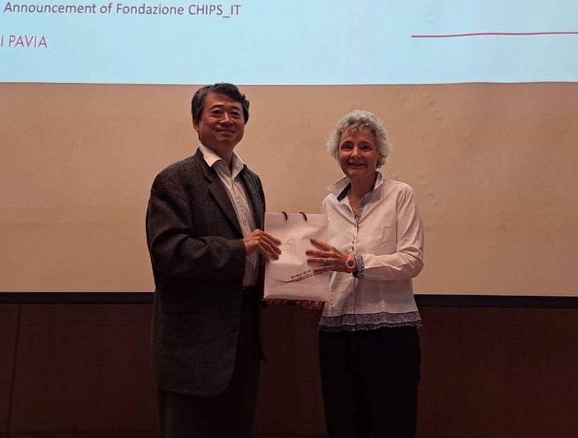
时间:
|
2023年9月8日(星期五)下午3时
|
|
讲者:
|
Prof. Sabina Merlo (Department of Electrical, Computer and Biomedical Engineering, University of Pavia, Italy)
|
|
讲题:
|
Electromechanical characterization of M(O)EMS by spot optical interferometric techniques
|
|
|
|
|
Prof. Sabina Merlo(右)与本所黄升龙教授(左)合影
|
|
|
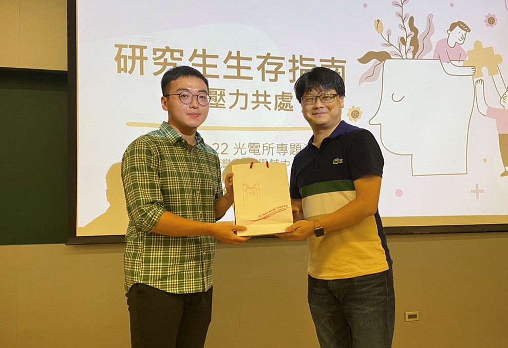
时间:
|
2023年9月22日(星期五)下午2时20分
|
|
讲者:
|
林子茗学辅专员(国立台湾大学学务处学辅中心)
|
|
讲题:
|
研究生生存指南—与压力共处
|
|
|
|
|
林子茗学辅专员(左)与本所李翔杰教授(右)合影
|
|
|
10月份「光电所专题演讲」
(整理:简璟)
|
|
时间:
|
2023年10月6日(星期五)下午2时20分
|
|
讲者:
|
叶秩光教授(国立清华大学生医工程与环境科学系)
|
|
讲题:
|
Acoustic vortex for confining light fluence
|
|
|
|
|
叶秩光教授(左)与本所李翔杰教授(右)合影
|
|
|
时间:
|
2023年10月13日(星期五)下午2时20分
|
|
讲者:
|
陈隆建教授(国立台北科技大学光电工程学系)
|
|
讲题:
|
Progress of all-inorganic perovskite quantum dot light-emitting diodes
|
|
|
|
|
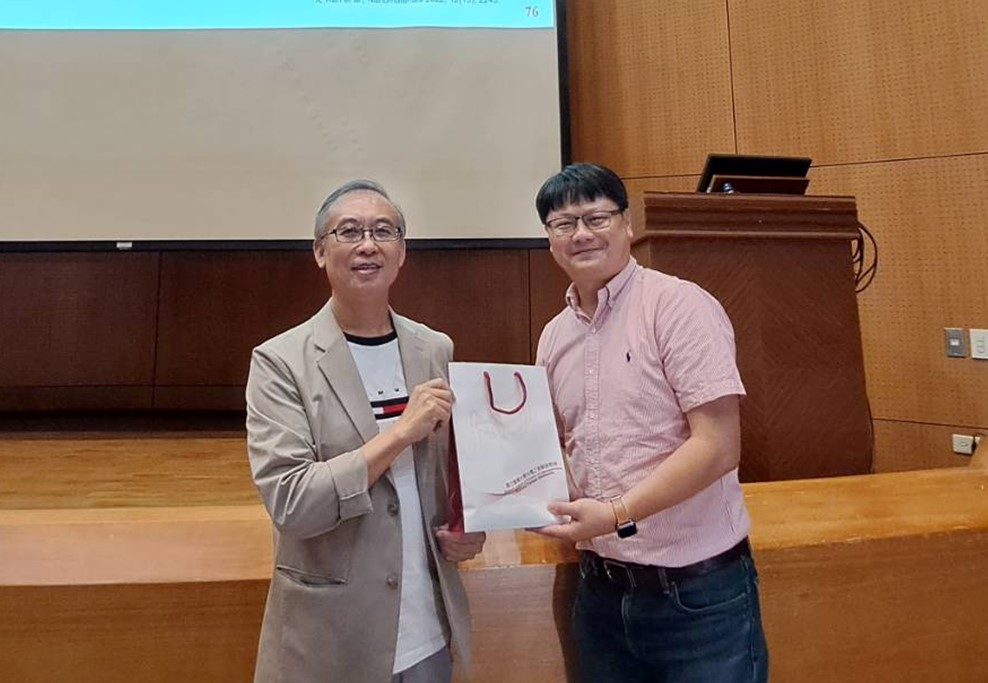
陈隆建教授(左)与本所李翔杰教授(右)合影
|
|
|
时间:
|
2023年10月20日(星期五)下午2时20分
|
|
讲者:
|
林晓均教授(国立清华大学生医工程与环境科学系)
|
|
讲题:
|
Light and Sound: Biomedical Optoacoustic Imaging
|
|
|
|
|
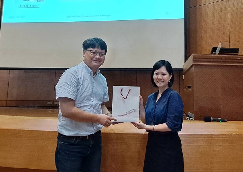
林晓均教授(右)与本所李翔杰教授(左)合影
|
|
|
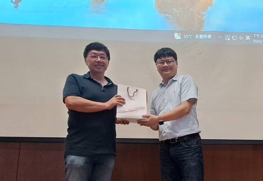
时间:
|
2023年10月27日(星期五)下午2时20分
|
|
讲者:
|
王万仓处长(友达光电前瞻技术中心)
|
|
讲题:
|
Flexible Technology Evolution: from Rigid to Flexible, and Beyond
|
|
|
|
|
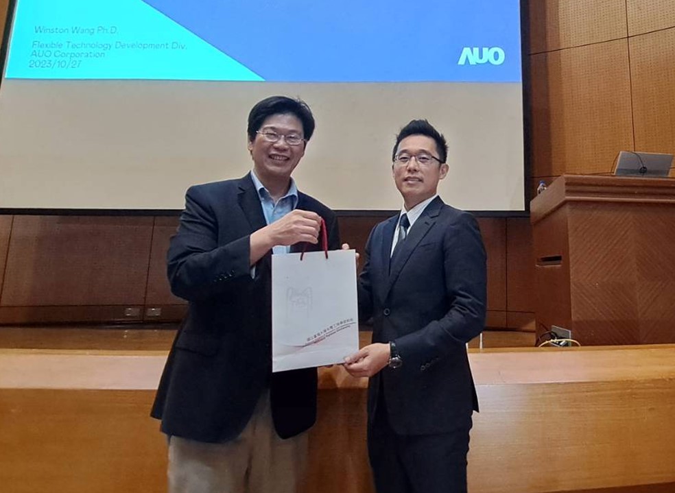
王万仓处长(右)与本所李君浩教授(左)合影
|
|
|
|
|
|
|
|
|
|
| |
|
|
|
|
|
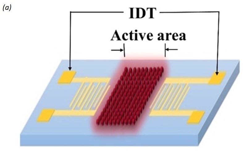
Manipulation of plasmonic relaxation possible by voltage-modulation
Professor Jian-Jang Huang's Laboratory
Graduate Institute of Photonics and Optoelectronics, National Taiwan University
台湾大学光电所 黄建璋教授
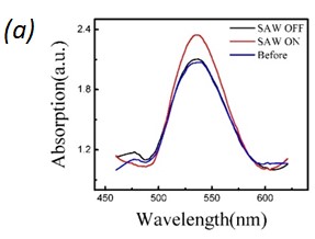
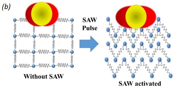
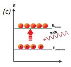
We experimentally study the effect of amplitude varying surface acoustic waves on localized surface Plasmon (LSP), which unveils exceptional properties of plasmon-phonon interaction with promising applications in future tunable photonic devices. Gold nanoparticles are deposited on an X-cut LiNbO3 to generate plasmonic oscillation, and an interdigital transducer is fabricated to create surface acoustic wave pulses. The interaction between amplitude varying mechanical wave and plasmonic oscillation affects different plasmon dynamics and relaxation gradients, leading to a systematic change in LSP absorption. We also demonstrated the effect of polarized light on the device, providing a unique characteristic to explore the manipulation process effectively.
|
|
|
|
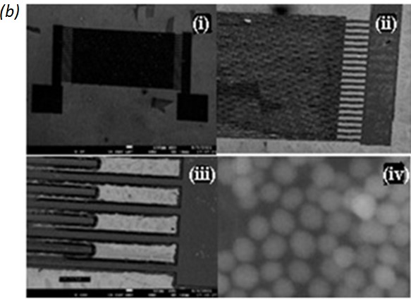
Fig. 1. (a) Illustration of the device, which is composed of a source IDT, randomly distributed Au nanoparticles and a receiving IDT. (b) (i) (ii) (iii) SEM images of fabricated IDT, (iv) Surface morphology captured by SEM where 40nm uniformly sized Au nanoparticles are distributed on the surface.
|
|
|
|
|
|
|
|
|
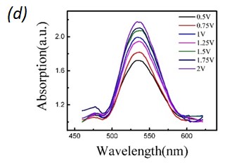
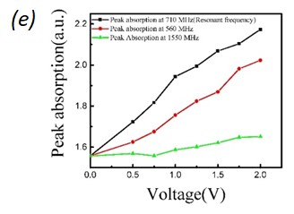
Fig. 2. (a) LSPR response with respect to different switching conditions of the IDT. Where the LSPR adsorption increase with SAW is On and retract back when SAW is off. (b) Diagram of phonon-plasmon interaction with and without SAW activated acoustic phonons. The plasmonic electron density increases with the applied SAW pulse as compared to the case without SAW. (c) Illustration of SAW activated electron transition to the plasmonic state. The SAW activated phonons participate in phonon-plasmon coupling and increase the plasmonic population. (d) Change of LSPR absorption with varying amplitude of SAW. (e) Amplitude varying LSPR response with respect to different SAW resonant conditions, where at the SAW resonant frequency (710 MHz) the change of LSPR absorption is highest.
|
Low-Temperature HfZrO2 Ferroelectric Thin-Film Transistors with a-InGaZnO Channels
Professor I-Chun Cheng
Graduate Institute of Photonics and Optoelectronics, National Taiwan University
台湾大学光电所 陈奕君教授
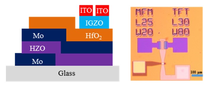
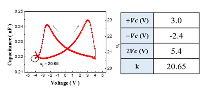
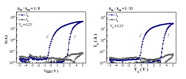
Owing to the relatively low process temperatures, HfO2-based ferroelectric materials integrated with oxide-based thin-film transistors have been considered as potential candidates for back-end-of-line compatible ferroelectric field-effect transistors, which can be vertically stacked on silicon CMOS circuits to realize high-density neural network applications or implemented on various types of substrates for novel applications. It is known that the formation of ferroelectric orthorhombic phase in HfO2-based materials can be strongly influenced by the annealing temperature, the thickness of film and the types of top and bottom metallic electrodes. In this work, low-temperature ferroelectric thin-film transistors (Fe-TFTs) were developed by monolithically integrating HfZrO2 (HZO) ferroelectric capacitors with amorphous indium gallium zinc oxide (a-IGZO) TFTs on glass substrates. Figs. 1(a) and (b) show the schematic diagram and microscopic photograph of the on-glass FeTFT, respectively. The Fe-TFT has a metal-ferroelectric-metal-insulator-semiconductor structure. The HZO ferroelectric layer was deposited by atomic layer deposition. The a-IGZO channel layer was deposited by rf-sputtering. The maximum process temperature is 350°C. A butterfly-shaped capacitance-voltage curve is observed, as shown in Fig. 2, revealing the top and bottom Mo electrodes can introduce sufficient mechanical stress to induce the formation of ferroelectricity in the HZO layer after annealed at 350°C. The positive and negative coercive voltages are 3 V and -2.4 V, respectively. The dielectric constant is 20.65. Fig. 3 shows the transfer hysteresis curves of the low-temperature HZO Fe-TFTs. The Fe-TFTs exhibit large hysteresis memory windows of 2.8 V and 3.8 V when the area ratios between ferroelectric capacitors and gate insulators are 1/8 and 1/12, respectively.
|
|
|
|
Fig. 1. (a) Schematic diagram and (b) optical micrograph of HZO Fe-TFT with a-IGZO channel.
|
Fig. 2. Capacitance-voltage curve & dielectric constant of low-temperature annealed HZO ferroelectric capacitor.
|
|
|
|
Fig. 3. Transfer hysteresis curves of HZO FeTFTs with (a) AFE / ADE = 1 / 8 and (b) AFE / ADE = 1 / 12. The Fe-TFTs are operated at VDS = 0.2 V.
|
|
|
|
|
|
|
|
|
|
| |
|
|
|
|
|
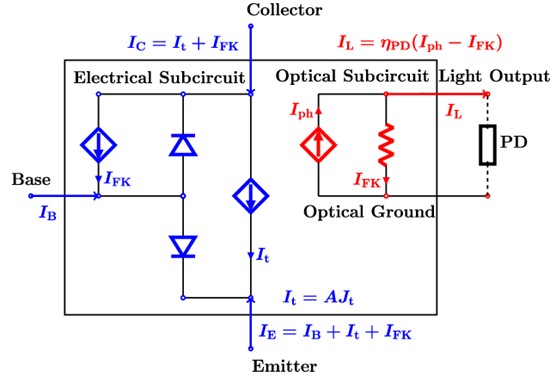
论文题目:适用于系统以及电路仿真的异质接口双载子发光敏晶体管模型
姓名:杨顺 指导教授:吴肇欣教授
|
摘要
|
|
异质结双极发光敏晶体管(也称为 LET 和 HBLET),基于量子井的异质结双极发光晶体管由于其具有多端口操作能力,因此能够作为光通信和光电集成电路(OEIC)中的候选器件。
从器件物理开始,我们构建了发光敏晶体管模型,用于光电集成电路和电气设计自动化的仿真和使用。除了对器件功能很重要的发光敏晶体管基本特性之外,我们的模型还准确描述了发光敏晶体管的电到电和电到光特性。还提供导纳矩阵,用于调制响应的通用模拟,包括散射参数和电流增益。为了确保电路仿真器SPICE兼容,还给出了发光敏晶体管的大信号眼图。在我们的模型的帮助下,可以加快电路设计的过程,这也可以帮助电路设计者分析自己电路的有效性。
本篇论文并模拟比较发光敏晶体管在热感应器,光收发器的效能。另外也运用TCAD仿真组件内部电流以及载子复合的分布,以及不同尺寸下的组件跟电路特性。
 |
 |
|
图一、发光电光晶体等效电路
|
图二、发光敏晶体管多模态热感应电路
|
|
|
|
|
|
|
|
|
|
|
| |
|
|
|
|
|
— 资料提供:影像显示科技知识平台 (DTKP, Display Technology Knowledge Platform) —
— 整理:林晃岩教授、林珈庆 —
芯片上的微波震荡器
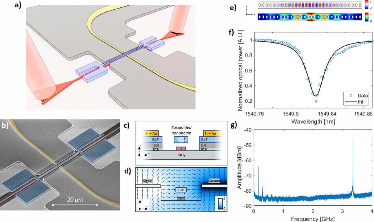
最新研究指出,光学芯片可能成为纯凈、低噪音微波信号之有前途的整合来源,适用于卫星通信和5G行动网络的应用。来自巴黎Saclay大学和法国公司Thales的Róbert Hórvath及其同事们在实验中证明,由光激发的磷化镓悬浮奈米横梁可在3.35 GHz的频率下作为高性能振荡器(Róbert Hórvath, et al.,” Sub-Hz Closed-Loop Electro-Optomechanical Oscillator with Gallium Phosphide Photonic Crystal Integrated on SoI Circuitry,” ACS Photonics, 2023)。特别是,该来源在尺寸为30 × 0.7 μm2的芯片上具有约0.7 Hz的线宽和约–111 dBc Hz-1的相位噪音。
这个集成在绝缘体上硅之光学电路上的镓磷化物(GaP)奈米横梁,经过精心设计的孔洞模式,使其成为一个一维光子晶体腔。这个腔体具有强烈的光机耦合,可以有效地限制光学模态和千兆赫机械模态。当以1,550 nm的共振波长的光透过光学波导被注入腔体时,它会激发腔体的机械模态,这种模态会对光学信号进行调变,并有效地被印刻在信号上。随后,光学信号从腔体中送出,然后由连接到光电二极管的电谱分析仪进行检测,清楚地显示在3.35 GHz处有一个单一而尖锐的峰值。
|
|
|
图一、在绝缘体上硅之光学电路上制作镓磷化物(GaP)奈米横梁,成为一个一维光子晶体腔。(a) 组件示意图;(b) 组件照片;(c) 剖面图;(d)(e) 场图;(f)(g) 频谱图。
|
参与该研究的研究人员之一Rémy Braive评论道:「我们的设计结合了III-V族材料在电光机械方面的优势和硅平台在可制造性和集成性方面的优点,此外,与其它微波振荡器相比,它的占用空间小,耗能低。」
进一步的功能是透过使用在芯片上的金电极引入的,这些电极分别位于镓磷化物(GaP)奈米横梁的两侧,相距1μm,当施加电压于横梁上时,可以在横梁长度的垂直方向上创造一个横向的电场。由于镓磷化物具有压电性,施加的电场可以直接引入电机耦合作用,以帮助调整设备的响应。为了提高振荡的质量,法国研究团队实施了一个电光死循环反馈回路,其中包括一段长度为210米的光纤作为延迟线,以及应用于电极的射频信号。Braive解释道:「我们未来的计划是使用声子相对于光子的缓慢传播的特性,在芯片上集成延迟线。」
|
参考资料:
|
Graydon, O., "Microwave oscillator on a chip," Nature Photonics 17, pages 648 (2023)
https://doi.org/10.1038/s41566-023-01259-0
DOI:10.1038/s41566-023-01259-0
|
|
参考文献:
|
Róbert Hórvath, et al., "Sub-Hz Closed-Loop Electro-Optomechanical Oscillator with Gallium Phosphide Photonic Crystal Integrated on SoI Circuitry," ACS Photonics 10, No. 8, pages
2540–2548 (2023)
https://doi.org/10.1021/acsphotonics.3c00074
DOI:10.1021/acsphotonics.3c00074
|
|
|
|
|
|
|
|
|
|
|
|
|
|
|
 |
|
 |
|