|
Bi-directionally Tunable Arrayed Waveguide Grating with Ultra-low Thermal Power
Professor Ding-Wei Huang
Graduate Institute of Photonics and Optoelectronics, National Taiwan University
台湾大学光电所 黄定洧教授
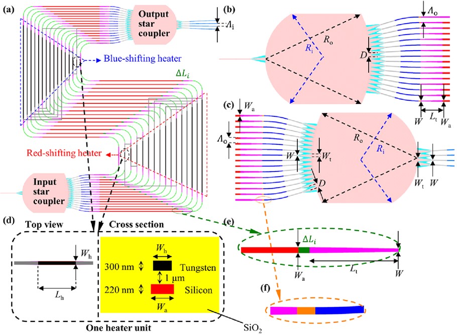
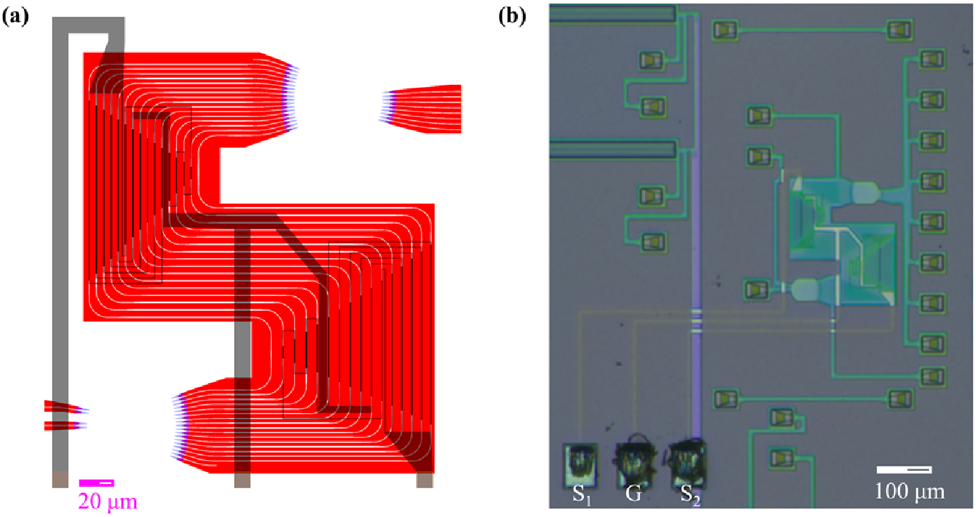
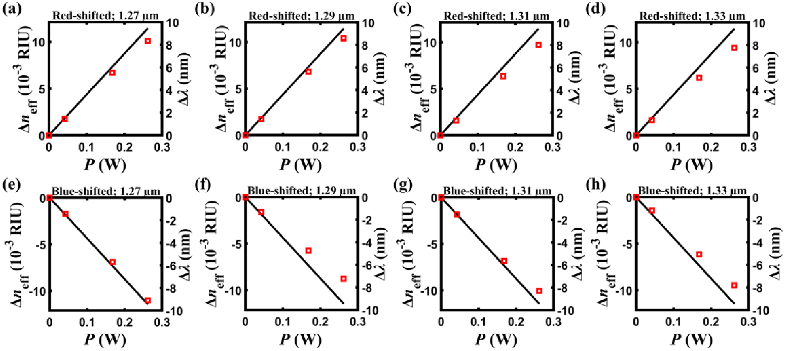
A thermally bi-directionally tunable arrayed waveguide grating (TBDTAWG) is proposed and demonstrated on a silicon-on-insulator (SOI) platform (Fig. 1). The device is composed of passive and active designs for realizations of an AWG and fine tuning of its filtering responses. Given that the required length difference between adjacent arrayed waveguides for the SOI platform is considerably short (∼3–5 µm) due to a high index contrast, an S-shaped architecture with a larger footprint instead of a rectangular one is employed in the AWG (Fig. 2). Bi-directionally tunable functions, i.e., both red- and blue-shift tunable functions, can be achieved by using two triangular thermal-tuning regions with complementary phase distributions in the S-shaped architecture despite using only materials with positive thermo-optic coefficients, i.e., Si and SiO2. Measurement results illustrate that both red- or blue-shifted spectra can be achieved and a linear bi-directional shift-to-power ratio of ±30.5 nm/W as well as a wide tuning range of 8 nm can be obtained under an electrical voltage range of 0–2.5 V, showing an agreement between the measurement results and two-dimensional simulation results (Figs. 3 and 4). This also shows the potential of the proposed TBDTAWG for automatically stabilizing the spectral responses of AWG-based (de)multiplexers for coarse or dense wavelength division multiplexing communication systems by using a feedback control circuit.
|

|
|
Fig. 1. Schematic top view of (a) overall TBDTAWG, (b) input star coupler, (c) output star coupler, (d) magnified top view and cross section of one heater unit, (e) magnified length difference (dark green), and (f) magnified straight waveguide (orange).
|
|

|
|
Fig. 2. (a) Mask layout of the proposed TBDTAWG and (b) photograph of the fabricated device on the SOI chip.
|
|

|
|
Fig. 3. (a) Red-shifted and (b) blue-shifted filtering responses for different applied voltages of 0, 1, 2, and 2.5 V are represented by solid, dashed, dotted, and dash-dotted lines, respectively.
|
|

|
|
Fig. 4. The linear relationship between the spectrum shifts and the required thermal powers at four output Channels 1.27, 1.29, 1.31, and 1.33 µm for (a–d) red-shift tuning and (e–h) blue-shift tuning, where the solid line and squared red marker represent the simulated results from Fig. 4 and the measured data from Fig. 6, respectively.
|
Design and Realization of a Wide Field-of-view Scanning LiDAR Based on MEMS Mirror
Professor Guo-Dung Su
Graduate Institute of Photonics and Optoelectronics, National Taiwan University
台湾大学光电所 苏国栋教授
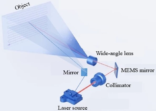
Light Detection and Ranging (LiDAR) sensor technology is the main driving force for automated transportation. Through the fusion of LiDAR sensor data, radar and camera lens, the surrounding environment can be fully and robustly sensed. However, most of today's LiDAR solutions are very complex and costly, and cannot effectively achieve scanning with a large field of view, so they cannot be widely used in vehicles and robots. We simulated and demonstrated a complete LiDAR system to solve the current obstacles to the development of MEMS LiDAR. By combining a MEMS mirror and a wide-angle lens into the scanning system, a low-cost, small-volume, and large-field-of-view LiDAR system can be realized. First, use ZEMAX OpticStudio optical simulation software to design a group of aspherical optical systems on the basis of scanning and widening optics to achieve the purpose of expanding the scanning angle of light. After the laser beam passes through this group of wide-angle lenses, the scanning angle can be expanded 4 times to 100 degrees. The distortion of the wide-angle lens is controlled below 3%, making the scanned image closer to the real situation. Second, in order to demonstrate low-cost, small-volume MEMS scanning LiDAR, a modular laser rangefinder (LRF) is used and a MEMS mirror is added. The entire system is erected on a self-designed and manufactured support. The complete prototype of LiDAR scanner is less than 150mm×50mm×30mm. The weight is less than 250 grams. In the 2klux natural light environment for wide-angle LiDAR measurement and analysis, the maximum error is 4.1cm, so the error is within 2%. Finally, a self-written image processing program was used to convert the scanned data into a 3D point cloud image, and the generated image proved the complete function of LiDAR.
|

|
|
Fig. 1. Combining an off-shelf single-point range finder, a MEMS mirror, and a wide-angle lens into the system, small-volume and large field-of-view (FOV) LiDAR systems can be realized.
|
Phosphor-doped fluorophore as dark sensitizer for blue triplet-triplet annihilation upconversion organic light-emitting diode
Professor Jiun-Haw Lee
Graduate Institute of Photonics and Optoelectronics, National Taiwan University
台湾大学光电所 李君浩教授
By doping 8% green phosphor, tris[2-phenylpyridinato-C2,N]Iridium(III) (Ir(ppy)3), into green fluorophore, tris-(8-hydroxyquinoline)aluminum (Alq3), a dark sensitizer (DS) was achieved for a blue organic light-emitting diode, consisting of triplet-triplet annihilation (TTA) emitter, 9,10-bis(2’-naphthyl) anthracene (ADN). Carriers recombined at Alq3 molecules which formed 25% singlets and 75% triplets. 25% Alq3 singlets underwent intersystem crossing to Ir(ppy)3 triplets followed by triplet energy transfer (TET) to Alq3 triplets, which resulted in 100% triplets in total, for TTA process which generate efficient blue emission. No fluorescence emission from green sensitizer was observed which efficiently improved external quantum efficiency of blue emission.
|