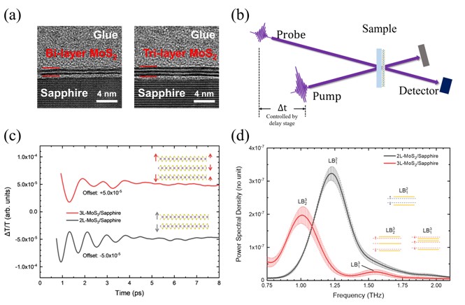
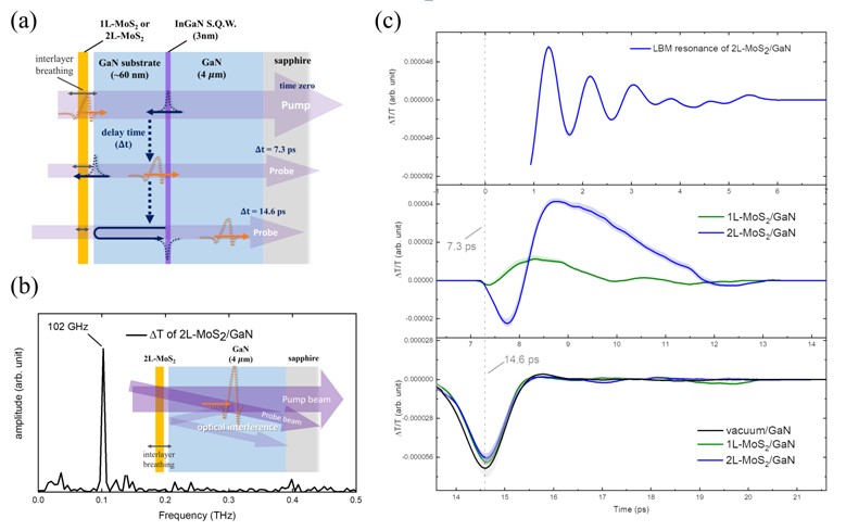
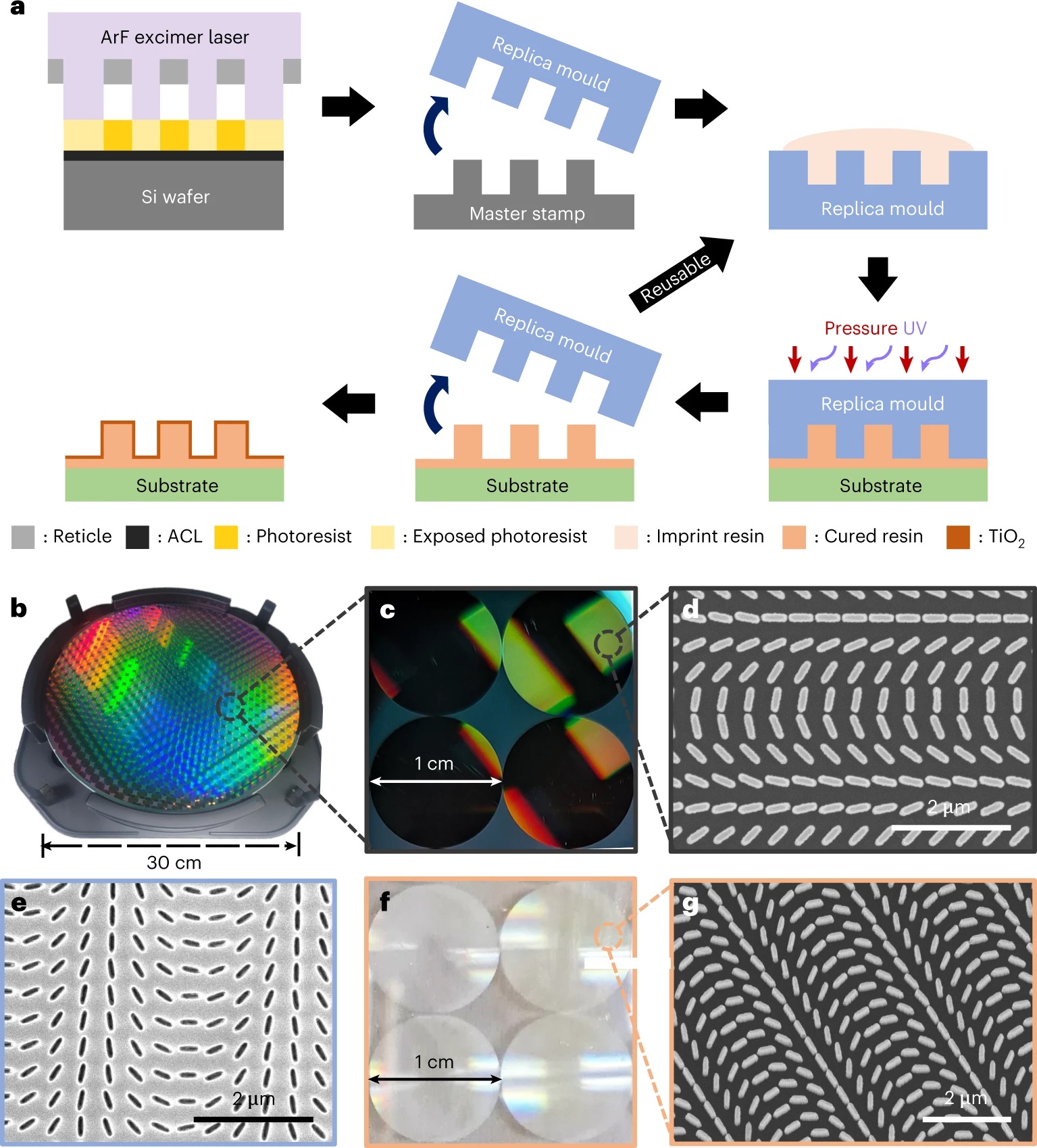
|
The Progress in the Colloidal Quantum Dot Based Color Conversion Layer
Professor Chien-chung Lin
Graduate Institute of Photonics and Optoelectronics, National Taiwan University
臺灣大學光電所 林建中教授
The progress in the past few years has put micro LED and related technologies in the roadmap for the next generation of smart displays. One of the key issues is the realization of a full-color display with a reasonable power consumption and footprint. The color conversion mechanism was often discussed in this direction and several labs around the world have demonstrated that this is feasible. There are many examples that can show great effects of color conversion: phosphors, chemical dyes, light emitting organic materials or inorganic colloidal quantum dots (CQDs). Although these materials can usually reach a conversion efficiency of 60 or 70% or even higher, the incapability of micro-pattern has become a major problem for all. In order to pattern them into an array of pixels, we have to either cast these materials accurately one by one or to mix them with photosensitive resin. Either way takes tremendous efforts to achieve good results. Among these color conversion materials, colloidal quantum dots are very promising due to their high conversion efficiency and small sizes. In our lab, we focus on two methods of these nanoparticles [1-3]: direct dispense and mixing CQD with photoresist. With the collaboration between our lab and the ITRI team, we demonstrated several different results of CQDs with micro LEDs previously [1-3].
|
|
|
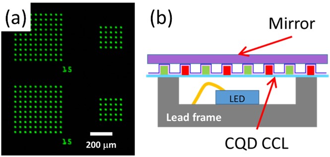
Fig. 1. (a) arrays of CQD pixels under the FLOM [4]; (b) the experimental setup [4].
|
Recently, the team from GIPO (Prof. Chung-Chih Wu and us) and from NYCU(陽明交通大學)worked together to demonstrate a semiconductor grade color conversion layer [4]. The distance between the pixels can be determined by the semiconductor grade of process which can improve the accuracy of the array greatly. The direct dispense method can ensure the highest concentration of CQDs presenting in each pixel. At the same time, we applied a reflective mirror on the top of this color conversion layer to enhance the photon recycling and a more-than-35% increase of CQD emission peak intensity was recorded. The corresponding numerical model was also developed under the incoherent reflection and transmission consideration. The result was just published in IEEE Photonics Journal and its website is: https://ieeexplore.ieee.org/abstract/document/10149805.
Reference:
[1] K.-L. Liang, W.-H. Kuo, H.-T. Shen, P.-W. Yu, Y.-H. Fang, and C.-C. Lin, "Advances in color-converted micro-LED arrays," Japanese Journal of Applied Physics, vol. 60, no. SA, p. SA0802, 2020/10/16 2020, doi: 10.35848/1347-4065/abba0f
[2] C.-C. Lin, K.-L. Liang, W.-H. Kuo, H.-T. Shen, C.-I. Wu, and Y.-H. Fang, "Colloidal Quantum Dot Enhanced Color Conversion Layer for Micro LEDs," IEICE Transactions on Electronics, vol. E105.C, no. 2, pp. 52-58, 2022, doi: 10.1587/transele.2021DII0005
[3] Y.-M. Huang et al., "The Aging Study for Fine Pitch Quantum-Dot Array on LEDs," in Conference on Lasers and Electro-Optics, San Jose, California, 2019/05/05 2019: Optical Society of America, in OSA Technical Digest, p. SF2O.2, doi: 10.1364/CLEO_SI.2019.SF2O.2
[4] G. Y. Lee et al., "Photonic Characterization and Modeling of Highly Efficient Color Conversion Layers With External Reflectors," IEEE Photonics Journal, vol. 15, no. 4, pp. 1-10, Art no. 2201110, 2023, doi: 10.1109/JPHOT.2023.3285667
|