|
|
 |
| |
发行人:吴育任所长 编辑委员:曾雪峰教授 主编:林筱文 发行日期:2022.08.30 |
| |
|
 |
30 GHz Highly Damped Oxide Confined Vertical-Cavity Surface-Emitting Laser
Professor Chao-Hsin Wu
Graduate Institute of Photonics and
Optoelectronics, National Taiwan University
台湾大学光电所 吴肇欣教授
Oxide-confined 850-nm vertical-cavity surface-emitting lasers (VCSELs) are reliable light sources for short-reach multi-mode optical communication applications due to their high efficiency, ease of fabrication, reliability, and small foot-print. 850 nm VCSELs with non-return-to-zero (NRZ) and 4-level pulse amplitude modulation (PAM-4) modulation have provided backbone optical interconnects for 400 and 800 Gigabit Ethernet networking technologies. The dramatically increasing data demand drives the VCSEL-based multi-mode fiber (MMF) links to equip advanced modulation schemes such as PAM-4, which puts specific emphasis on the dynamics performance of VCSELs, such as high bandwidth at low current, sharp edge in S21 response, and low intrinsic noise. Various methods have been investigated to reduce the device parasitics, increase modulation bandwidth and yield highly damped modulation responses.
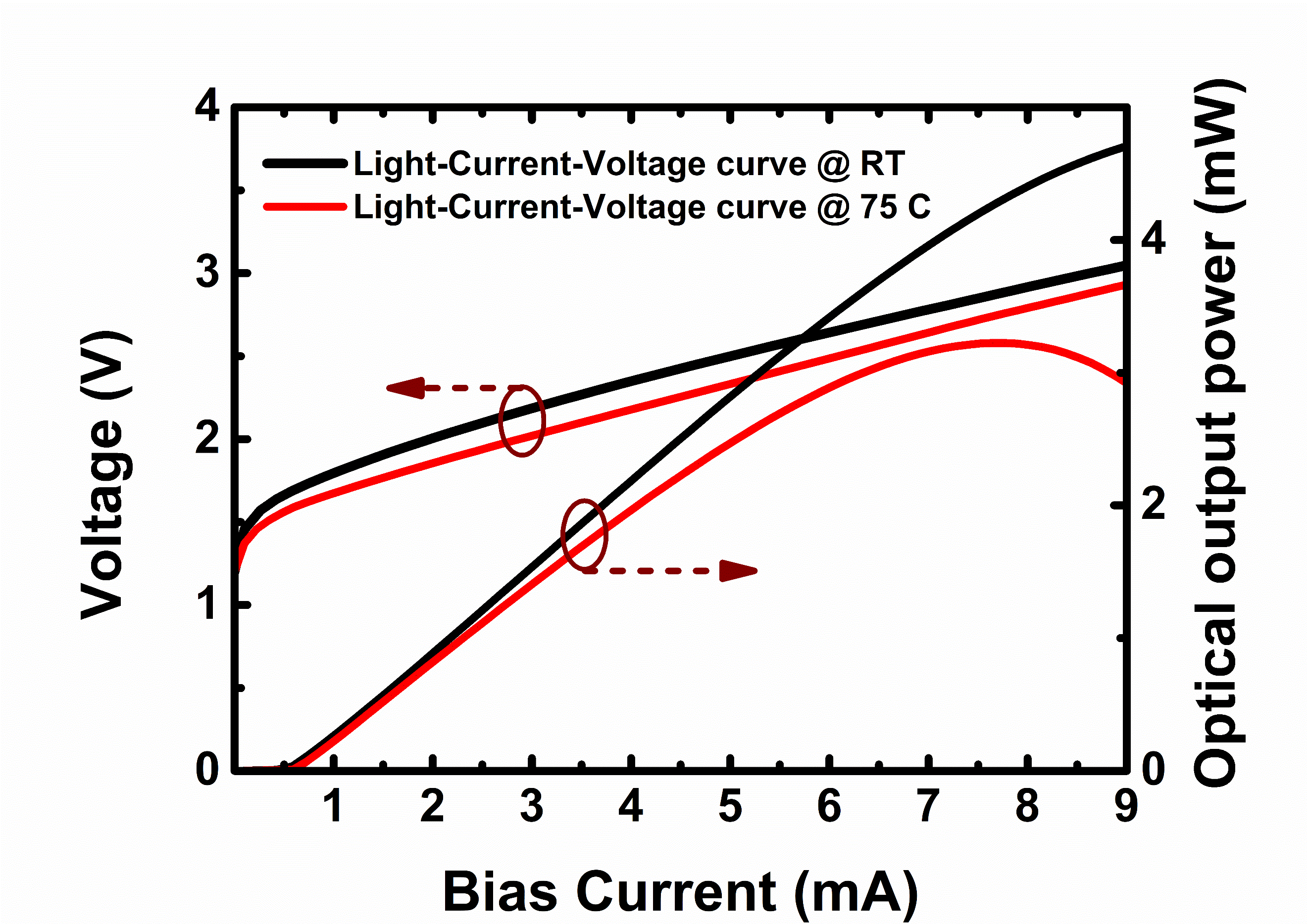
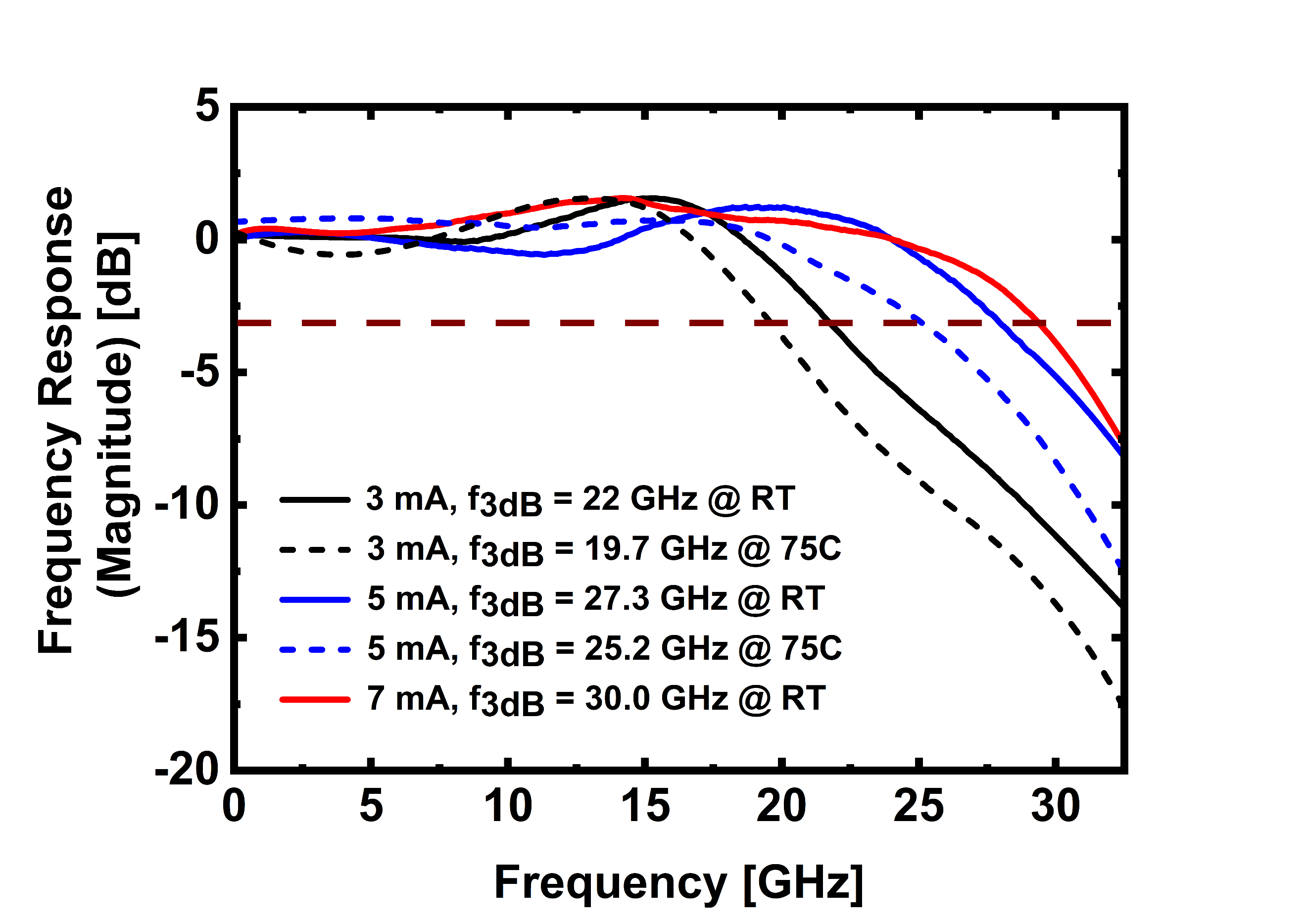
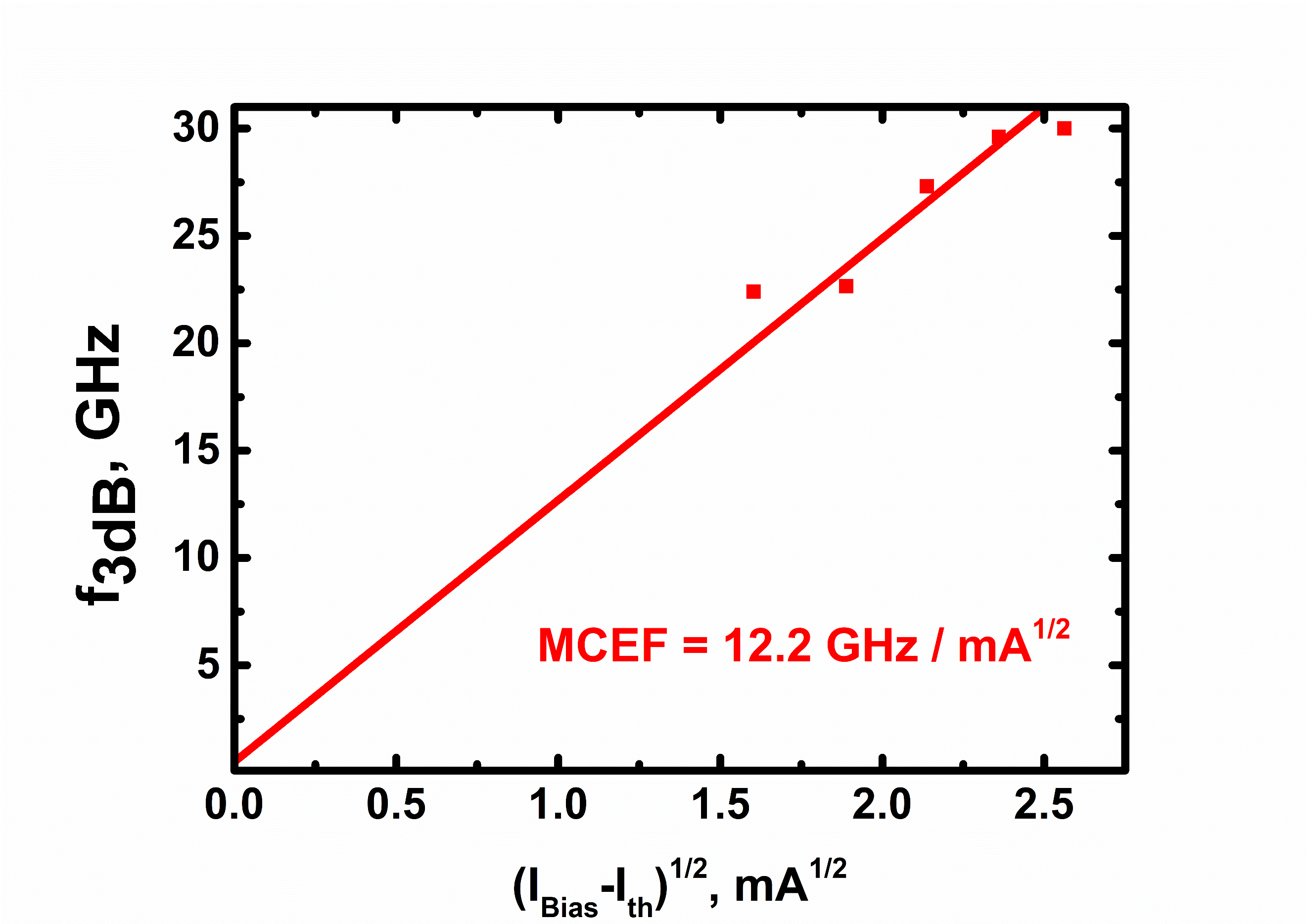
Our device employs six-pairs thick oxide aperture for a reduced device parasitics capacitance and an optimized relaxation oscillation damping with currents for high quality eyes at the targeted data rates. The highly-damped VCSEL exhibits a low thermal impedance, ultra-high bandwidth, and delivers a flat modulation response. The L-I-V curve of our high damped VCSEL with 3.5 μm oxide aperture at room temperature (RT) and 75°C is shown in Fig. 1. The VCSEL exhibit a peak optical power of 3.88 mW and roll-over current over 9 mA. Fig. 2 shows the measured modulation responses and the VCSEL exhibits flat modulation responses at various biases at RT and 75°C. When biased at 5 mA, the VCSEL reached 27.3 GHz and 25.2 GHz at RT and 75°C respectively, and showed a mere 2.1 GHz decrease in modulation bandwidth at the elevated temperature. The fitted MCEF is 12.2 GHz / mA1/2 and is illustrated in Fig. 3. We have demonstrated an ultra-fast highly damped VCSEL with a flat modulation response for up to 30 GHz. We employed several optimizations in the design of the VCSEL, including the intrinsic dynamic performance, RC parasitics, and photon lifetime tuning, which enable a thermally-stable operation for up to 75°C. The flat modulation characteristics of the VCSEL could enable over 100 Gb/s line rates PAM-4 modulation for 400G and 800G high-capacity optical interconnect systems.
|
|
|
Fig. 1. The L-I-V characteristics for a ~3.5 μm oxide aperture diameter at RT and 75°C. |
|
 |
|
Fig. 2. The S21 optical response when 3 mA, 5 mA, and 7 mA at RT and 75°C. |
|
|
|
Fig. 3.
3 dB bandwidth plotted against square root of biased current and MCEF fits. |
Step-shaped electrode for Blue Phase transflective liquid crystal displays
Professor Wing-Kit Choi
Graduate Institute of Photonics and
Optoelectronics, National Taiwan University
台湾大学光电所 蔡永杰教授
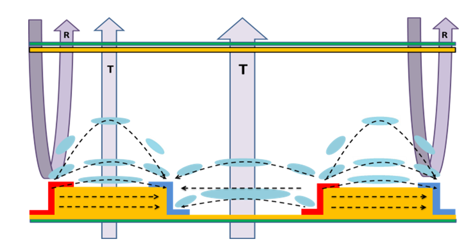
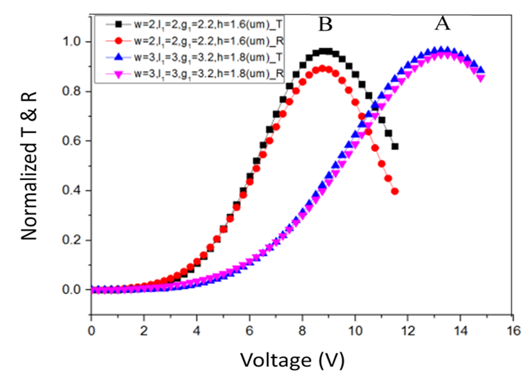
In recent years, our laboratory has been proposing new electrode designs for blue phase liquid crystal displays (LCDs) with high light efficiency and low operation voltage. One such design is shown in figure 1 below for a transflective LCD. We named this design “step-shaped electrode”. By using this design, it is possible to produce a blue-phase transflective LCD with very high light efficiency of > ~ 95% at low operation voltage of ~ 9 to 13V with well-matched T-V and R-V electro-optic curves as shown in figure 2. This design is based on the concept of forming fairly strong and uniform horizontal electric fields above the reflective (R) region which has a step-shaped reflective electrode and also above transmissive (T) region which is enhanced by the vertical wall-like electrode. These strong electric fields help minimize the dead-zones which normally exist above electrodes (as illustrated in figure 3) and hence enhance the transmission/reflection and lower the operation voltage.
|
|
|
Figure 1.
Structure of a blue-phase transflective LCD with step-shaped electrodes |
|
|
|
Figure 2. Normalized transmission (T) and reflection (R) of step-shaped electrode blue-phase transflective
LCD with
two
matched
designs
A and B |
|
|
|
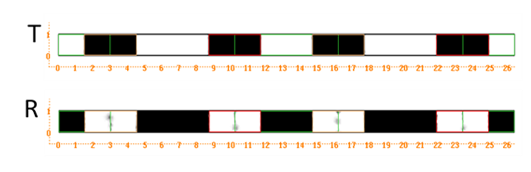
Figure
3. Top-view transmission (T) and reflection (R) profiles of a step-shaped electrode blue-phase transflective
LCD
showing
almost
no dead
zone
exist
above
electrodes |
|
 |
| |
|
|
|
 |
|
| |
|
|
|
—
数据提供:影像显示科技知识平台 (DTKP, Display Technology
Knowledge Platform) —
—
整理:林晃岩教授、吴思洁 —
快车道上的光
在超快时间尺度上对光子脉冲的成形,使光与原子和电子运动之间受控的交互作用成为可能。目前文献上已经建立了许多方法来进行具有皮秒(picosecond),甚至飞秒(femtosecond)分辨率的超快激光脉冲的相位和/或振幅工程。
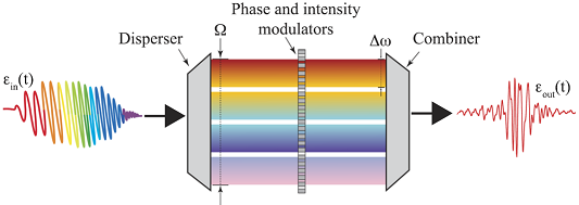
例如:傅立叶合成技术可用于对脉冲进行成形,就像利用频率梳的方法一样。任意波形也可以透过光的色散、适当调制部分光谱并将光重新组合成工程化波形。虽然这种方法在可能的波形方面非常灵活,但任意性取决于色散器的光谱分辨率和总光谱带宽,如图1。
|
|
|
图1、波形合成的概念 |
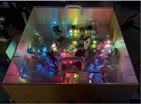
现在,在美国和德国工作的团队,Husain Alqattan、Dandan Hui、Vladimir Pervak 和 Mohammed Hassan已经克服了之前的挑战,并展示了跨越两个八度音阶的超连续谱的光场合成(APL Photon.
7, 041301; 2022)。这一发展将合成能力扩展到深紫外光谱区域。这些发现能够合成具有阿秒(attosecond)分辨率的光形,这对亚飞秒(sub-femtosecond)电子运动控制具有重要意义。
|
|
|
图2、阿秒光场合成器(Attosecond Light Field Synthesizer, ALFS)的展示图 |
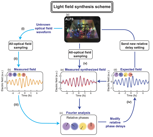
在解释这项工作的最初动机时,通讯作者Mohammed Hassan告诉Nature Photonics,他们的目标是在实际时间和空间中电子运动的成像和控制。而且,由于可以透过驱动器光场的依需求成形来实现电子运动的控制,因此他们有动力创建阿秒光场合成器(Attosecond Light Field Synthesizer, ALFS)的工具,如图2。第二个目标是希望使用阿秒(attosecond)光脉冲来释放超快自由电子,以产生阿秒电子脉冲,并启用先前提出的阿秒电子显微镜,该显微镜可用于实现时间和空间成像电子运动。
Hassan向Nature Photonics解释道:「最有挑战性的是找到一种简单且直接的方法来对ALFS的合成波形进行采样,确实,有一些成熟的方法,例如阿秒条纹,但它们的要求很高。我们能够利用遵循驱动场的介电系统的反射率调制来克服这一挑战,并将超快科学界引入全光场采样方法。这种直接且简单的光场采样方法使我们能够为阿秒光场合成依需求建立方案。」如图3。
|
|
|
图3、依需求光波成形架构 |
该团队计划透过展示阿秒光学开关和对超快激光脉冲进行拍赫兹(petahertz)数据编码的能力,将他们的工作提升到一个新的层次。
|
参考数据: |
David F. P. Pile, “Light in the fast lane, ”
Nature Photonics 16, pages 409
(2022)
https://doi.org/ 10.1038/s41566-022-01017-8
DOI: 10.1038/s41566-022-01017-8
|
|
参考文献: |
Husain Alqattan, Dandan Hui, Vladimir Pervak, and Mohammed Th. Hassan, “Attosecond light field synthesis,”
APL Photon. 7, 041301
(2022)
DOI: 10.1063/5.0082958
|
|
|
|
|
|
|
|
|
|
|
|
|
|
|
|
|
|
|
|
|
|
|
 |
|
 |
|