|
|
 |
| |
發行人:黃建璋所長 編輯委員:曾雪峰教授 主編:林筱文 發行日期:2022.06.30 |
| |
|
 |
|

本所吳育任教授指導碩士生張雨倢、沈雈莛同學榮獲「The 5th International Workshop on Ultraviolet Materials and Devices (IWUMD 2022) Best Poster Paper Award」,特此恭賀!
|
|
 |
|
 |
|
| |
|
|
|
Study of Current Collapse Behaviors of Dual-gate AlGaN/GaN HEMTs on Si
Professor
Jian-Jang Huang’s Laboratory
Graduate Institute of Photonics and
Optoelectronics, National Taiwan University
臺灣大學光電所 黃建璋教授
Surface traps on GaN-based HEMTs (high-electron-mobility transistors) usually
result in the increase of channel on-resistance. It becomes worsen when short
pulses are applied during high-frequency and high voltage switching. Here we
present a dual-gate transistor structure to suppress the dynamic on-resistance
increase. The auxiliary gate under a proper fixed voltage is able to induce
additional electrons to compensate the channel carrier loss during main gate
switching, leading to a lower dynamic on-resistance.
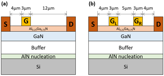
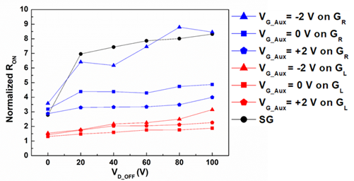
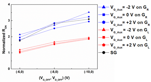
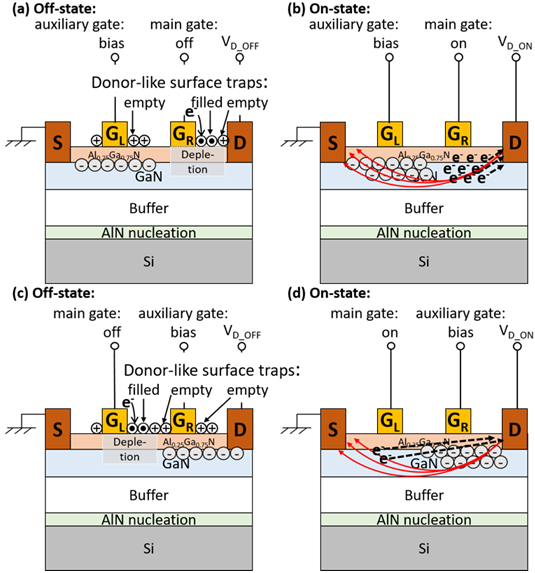
The dual-gate (DG) AlGaN/GaN HEMT is schematically shown in Fig. 1, along with a conventional device for comparisons. The DC electrical properties reveal that the drain current level of the DG-HEMT with GL-drive (main gate) and GR-float (auxiliary gate) is slightly higher than that of SG (single gate) -HEMT due to the additional carriers induced by the floating gate. The DG-HEMT with GR-drive and GL-float has the smallest current because of the largest gate-source resistance. When a bias voltage is applied on the auxiliary gate, the current level can be adjusted by the additional carriers. Since the auxiliary gate provides an extra source of supplying electrons to the channel that suffers from current collapse, we further studied current collapse phenomenon of the devices by a pulsed stress-measurement approach. The results suggest within the range of auxiliary gate bias, -2 ~ 2 V, a DG device with the main gate drive on GR and the auxiliary gate voltage of 0 V on GL has the lowest RON, while SG-HEMT is the worst in most of the stress conditions (see Fig. 2 for various drain and gate lag stresses). The improvement using the dual-gate structure is elucidated from the carrier distribution in the channel region as illustrated in Fig. 3. For the case main gate bias applied on GR and auxiliary bias on GL, the depleted carriers from the main gate can be quickly supplied by the carrier underneath the auxiliary electrode under a positive drain voltage with a slight negative impact of carriers recombined with traps on both sides of main gate. Finally, we conclude an auxiliary gate biased at 0 V near the source side results in the best suppress of current collapse.
|
|
|
Fig. 1. Cross-sectional epi-structure of (a) a SG-HEMT and (b) a DG-HEMT. |
|
 |
|
Fig. 2. (a) Comparison of the normalized RON at various drain stress voltages, VD_OFF, and auxiliary gate biases. |
|
|
|
Fig. 2. (b) Comparison of the normalized RON at various gate lag stress conditions. |
|
|
|
Fig. 3. Distribution of electrons in the channel under various biases on the main gate and auxiliary gate electrodes. GR-drive/GL-bias at (a) off-state and (b) on-state. GL-drive/GR-bias at (c) off-state and (d) on-state. Note there may be small amount of donor-like surface traps (not shown) on both sides of GL and GR, depending on the bias voltage of the auxiliary gate. |
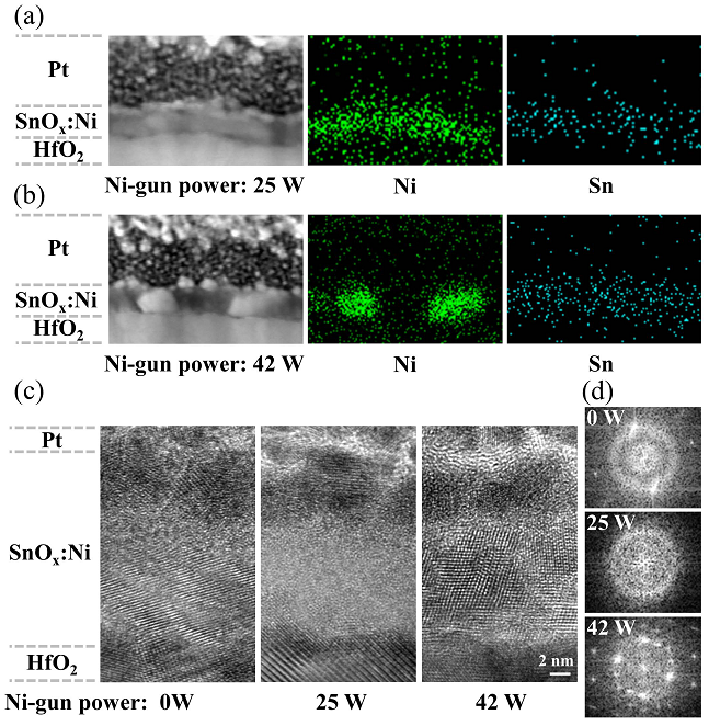
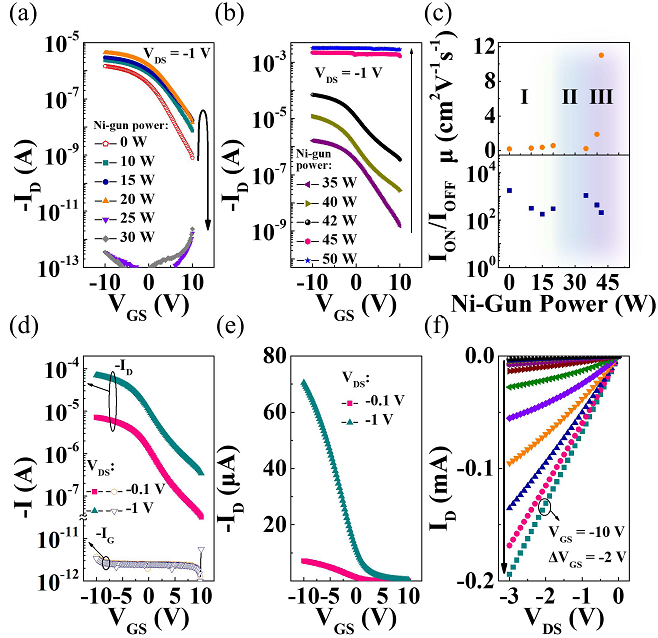
Mobility Enhancement in P-Type SnO Thin-Film Transistors via Ni Incorporation by Co-Sputtering
Professor I-Chun Cheng
Graduate Institute of Photonics and
Optoelectronics, National Taiwan University
臺灣大學光電所 陳奕君教授
Oxide semiconductors have been considered one of the most promising candidates for flexible electronics applications owing to their low process temperatures and good reliability. However, the low mobility of p-type oxide semiconductors limits the performance of flexible oxide-TFT-based CMOS technology. In this study, p-type SnOx:Ni thin films were deposited by reactive rf magnetron co-sputtering, a technique compatible with the current industrial semiconductor manufacturing technology, from Sn and Ni targets. As the Ni-gun power increased, the distribution of Ni in the SnOx:Ni thin film changed from a more uniform dispersion to nanoclusters, resulting in the crystalline phase transition of SnOx:Ni from
α-SnO (110)-dominant polycrystalline to amorphous and then to α-SnO (101)-dominant polycrystalline. A high-mobility inverted-staggered p-type SnOx:Ni TFT was then fabricated on a glass substrate with a maximum process temperature of 225°C, which is compatible with flexible polymeric substrates. The TFT fabricated at an optimal Ni-gun power of 42 W exhibited an impressive field-effect mobility of 11 cm2V−1s−1 and on current of 35.2 μA per channel width-to-length ratio; these values are comparable to those of a typical n-type oxide TFT. These results should contribute toward flexible oxide-TFT-based CMOS technology. [IEEE Electron Device Letters, vol. 43, No. 2, pp. 228-231, Feb 2022]
|
|
|
Fig. 1. Elemental EDS maps of SnOx:Ni thin films deposited at Ni-gun powers of (a) 25 and (b) 42 W. (c) High-resolution TEM images and (d) corresponding fast Fourier transformed diffractograms of SnOx:Ni channels deposited at Ni-gun powers of 0, 25, and 42 W. |
|
|
|
Fig. 2. (a)(b) Transfer characteristics of SnOx:Ni TFTs fabricated with various Ni-gun powers. The channel width and length are 40 μm and 20 μm, respectively. (c) Electrical parameters of SnOx:Ni TFTs under different Ni-gun powers. Transfer characteristics in (d) log scale and (e) linear scale and (f) output characteristics of SnOx:Ni TFT fabricated with a Ni-gun power of 42 W. |
|
|
| |
|
|
|
|
|
|
| |
|
|
|
—
資料提供:影像顯示科技知識平台 (DTKP, Display Technology
Knowledge Platform) —
—
整理:林晃巖教授、吳思潔 —
高效率的微型發光二極體
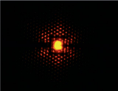
尺寸小於100×100 μm2的微米級發光二極體(μLED)有望成為擴增實境和虛擬實境等應用中之未來高解析度顯示器的關鍵技術。然而目前紅光μLED的外部量子效率(external quantum efficiency, EQE)僅為0.1%左右。因為存在許多問題,包括Shockley-Read-Hall非輻射復合、強量子限制史塔克效應(Stark effect)及較差的晶體品質。現在,來自美國加州大學聖塔芭芭拉分校的Panpan Li及其同事展示了5×5 μm2尺寸的InGaN μLED(如圖1),其發射波長為607 nm的琥珀色光,EQE最大值為2.6%(Appl. Phys. Lett. 120, 041102; 2022)。
透過大氣壓金屬有機化學氣相沉積(MOCVD),在極性c平面圖案化藍寶石基板上生長InGaN磊晶。藍寶石上刻有小圓錐(高度為1.7μm,直徑為2.6μm)。InGaN琥珀色μLED使用InGaN/GaN超晶格(superlattices)作為發光材料,並沉積Al/Ni/Au金屬作為電極,用以施加驅動電流。
μLED側壁區域發生的漏電流通常是由反應離子蝕刻(RIE)所造成的。為了抑制此問題,透過沉積30 nm厚的SiO2層來實現側壁鈍化。其鈍化的效果透過在施加-5 V的電壓下低至10-9 A的反向電流得到實驗證實。
InGaN琥珀色μLED在注入3 A cm-2的電流密度下在607 nm處具有一個峰值,光譜半高全寬為44 nm。3 A cm–2處的發射光譜對應於國際照明委員會1931色度圖中(x,y)點的(0.59, 0.36)處。隨著注入電流密度從0.5增加到70 A cm-2,電致發光的峰值波長呈現從617到570 nm的大量藍移。在20 A cm-2 下,輸出功率和光通量分別為0.27 μW和1.27×10⁻⁴ lm。
與許多其他LED一樣,μLED表現出效率下降的現象—當電流密度增加超過某個特定點時,EQE會下降。美國科學家通過製造5×5 μm2 和100×100 μm2 InGaN琥珀色μLED並比較它們的性能,研究了這種效率下降隨元件尺寸如何變化。5×5 μm2與100×100 μm2元件相比,EQE下降趨勢更大,這表明側壁毀損所造成的非輻射復合的影響。科學家們認為,可以透過降低缺陷密度來進一步提高InGaN琥珀色μLED的EQE。
|
|
 |
|
圖1、InGaN琥珀色光μLED與其發光照片 |
|
參考資料: |
Horiuchi, N. “Efficient microscale emitters”
Nature Photonics volume
16, pages264 (2022)
https://doi.org/10.1038/s41566-022-00984-2
DOI:10.1038/s41566-022-00984-2
|
|
參考文獻: |
Panpan Li, Hongjian Li, Yunxuan Yang, Haojun Zhang, Pavel Shapturenka, Matthew Wong, Cheyenne Lynsky, Mike Iza, Michael J. Gordon, James S. Speck, Shuji Nakamura, and Steven P. DenBaars, “Demonstration of ultra-small 5 × 5 μm2 607 nm InGaN amber micro-light-emitting diodes with an external quantum efficiency over 2%,” Appl. Phys. Lett. 120, 041102 (2022).
https://doi.org/10.1063/5.0078771
DOI:10.1063/5.0078771
|
|
|
|
|
|
|
|
|
|
|
|
|
|
|
|
|
|
|
|
|
|
|
 |
|
 |
|