|
|
 |
|
 |
| |
發行人:黃建璋所長 編輯委員:曾雪峰教授 主編:林筱文 發行日期:2022.02.28 |
| |
|
 |
|

本所蘇國棟教授指導碩士生劉思彤同學榮獲「2022年物理年會壁報論文優等獎」,特此恭賀!
壁報論文名稱:Heterodyne Sum-Frequency Surface Phonon Spectroscopy
|
|
 |
|
 |
|
| |
|
|
|
|
10月份「光電所專題演講」(整理:姚力琪) |
|
時間: |
110年10月1日(星期五)下午2時20分 |
|
講者: |
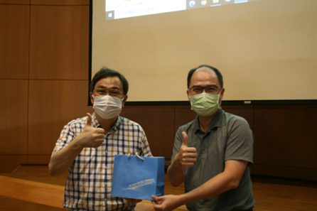
張鼎張講座教授(國立中山大學物理系) |
|
講題: |
低溫缺陷鈍化技術在半導體元件應用 |
|
 |
|
張鼎張教授(左)與本所所長黃建璋教授(右)合影 |
|
|
時間: |
110年10月15日(星期五)下午2時20分
〈※
線上演講〉 |
|
講者: |
陳階曉執行長(鈦隼生物科技股份有限公司) |
|
講題: |
Robots in OR, the Future is NOW |
|
|
|
|
時間: |
110年10月22日(星期五)下午2時20分 |
|
講者: |
陳啟東博士(中央研究院物理研究所) |
|
講題: |
Building a Superconducting Quantum Computer |
|
|
|
11月份「光電所專題演講」(整理:姚力琪) |
|
時間: |
110年11月5日(星期五)下午2時20分 |
|
講者: |
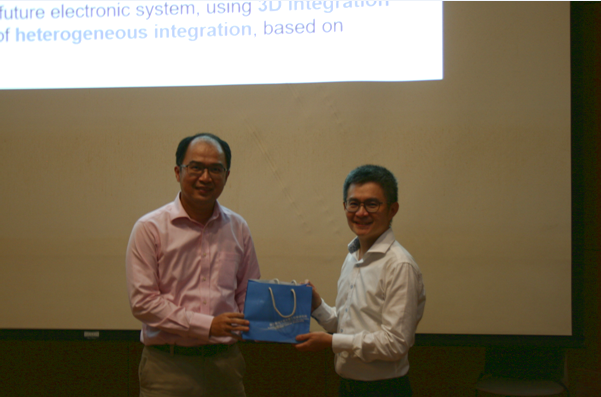
陳冠能講座教授(國立陽明交通大學電子研究所) |
|
講題: |
3D IC and Advanced Packaging |
|
 |
|
陳冠能教授(右)與本所所長黃建璋教授(左)合影 |
|
|
時間: |
110年11月12日(星期五)下午2時20分
〈※
線上演講〉 |
|
講者: |
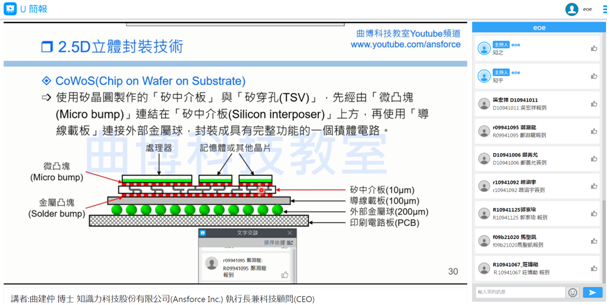
曲建仲博士(知識力科技股份有限公司 (Ansforce Inc.) 執行長兼科技顧問) |
|
講題: |
晶圓代工與先進封裝技術應用商機 |
|
|
|
時間: |
110年11月19日(星期五)下午2時20分
〈※
線上演講〉 |
|
講者: |
徐茂修博士(敦泰電子股份有限公司) |
|
講題: |
高速傳輸整合聲音、影像、資料、電力傳輸之方案IC設計 |
|
|
|
12月份「光電所專題演講」(整理:姚力琪) |
|
時間: |
110年12月10日(星期五)下午2時20分
〈※
線上演講〉 |
|
講者: |
吳文中教授(國立臺灣大學工程科學及海洋工程學系) |
|
講題: |
My IoT Journey. From research, startup to tech jobs. |
|
|
|
時間: |
110年12月17日(星期五)下午2時20分
〈※
線上演講〉 |
|
講者: |
蕭立人博士(國家中山科學研究院) |
|
講題: |
Beyond the Lab 課外研究 |
|
|
|
1月份「光電所專題演講」(整理:姚力琪) |
|
時間: |
111年1月14日(星期五)下午2時20分
〈※
線上演講〉 |
|
講者: |
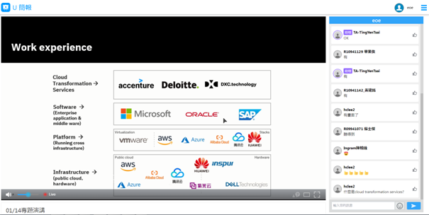
謝承哲先生(IBM Infrastructure specialist) |
|
講題: |
職涯轉換的權衡與經驗 |
|
|
|
|
|
|
|
|
|
|
|
|
| |
|
|
|
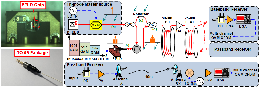
Coherent Tri-mode FPLD with SCM of 80 Gbit/s OFDM for 75-km Long-Reach MMWoF at 28 GHz
Professor Gong-Ru Lin’s Laboratory
Graduate Institute of Photonics and
Optoelectronics, National Taiwan University
臺灣大學光電所 林恭如教授
A novel FPLD with orthogonal polarized tri-mode under single-carrier modulation (SCM) for chromatic dispersion suppression is employed to demonstrate 28-GHz remote optical heterodyne in millimeter-wave-carrier-over-fiber (MMWoF) for 75-km long-reach wireline and wireless transmission at 80 and 30 Gbit/s under bit-loaded M-QAM OFDM with spectral usage efficiency up to 10 bit/s/Hz. The 28-GHz and 75-km long-reach MMWoF constructed by an orthogonal tri-mode LD with SCM is exhibited in Fig. 1. A single-polarization light source generated from a DFBLD was adjusted a 45o polarization between the light source and the Mach-Zehnder modulator (MZM). A 28-GHz LO sinusoidal wave was modulated onto the single-polarization light source by a MZM with null-point operation for the orthogonal tri-mode master source generation (point (a)). The orthogonal tri-mode master was divided into two paths by an optical coupler. One path of this master source injection-locked a Fabry-Perot LD (FPLD) only supporting the TE polarization. The side modes of the tri-mode source with the TM polarization would be suppressed in the FPLD cavity, which implements the SCM (point (b)). For another path, the central carrier of the tri-mode source was suppressed by a polarizer (node (c)). The injection-locked carrier and central-carrier suppressed side-modes source were orthogonal combined by another optical coupler to form an orthogonal tri-mode optical carrier with SCM (point (d)). The narrow-band 64- to 1024-QAM OFDM with the bandwidth from 166 to 100 MHz was generated by an 18-GSa/s AWG. The bit-loaded QAM-OFDM data was modulated on the injection-locked carrier with side-mode suppression by the FPLD as an optical amplifier and modulator.
|
|
|
Fig. 1. The microscopic image, package photo, and network scheme of a tri-mode FPLD with SCM of M-QAM OFDM for 75-km long-reach MMWoF. |
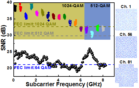
To maximize the transmission capacity and meet the 5G standard, the multi-channel bit-loaded M-QAM OFDM with 100-MHz/channel bandwidth is employed. The maximal channel number in 8-GHz bandwidth is obtained as 80, and the first channel is set from 70 MHz. After demodulation, the SNR spectra of each narrow-band bit-loaded M-QAM OFDM data and the wide-band 64-QAM OFDM data delivered by orthogonal tri-mode optical carrier after 75-km transmission are exhibited in Fig. 2. Figure
3 also shows the related constellation plots for the narrow-band bit-loaded M-QAM OFDM data. The maximal bandwidth and raw data rate of the delivered wide-band 64-QAM OFDM, which can pass the FEC limit, are obtained as 8 GHz and 48 Gbit/s, respectively. For the narrow-band case, the total raw data rate of the delivered multi-channel bit-loaded M-QAM OFDM data is evaluated as 10 (1024 QAM)
x6 GHz+9 (512 QAM) x2.2 GHz=80 Gbit/s.
|
|
|
Fig. 2. The SNR spectra of narrow-band M-QAM OFDM data and wide-band 64-QAM OFDM data delivered by orthogonal tri-mode optical carrier after 75-km transmission. |
|
 |
|
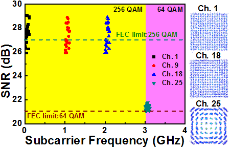
Fig. 3. The frequency spectra of the delivered multi-channel M-QAM OFDM by beat 28-GHz MMW carrier after 10-m free space transmission. |
The multi-channel bit-loaded M-QAM OFDM data with the same channel bandwidth is also employed at wireless transmission. After the same demodulation, the SNR spectra of each narrow-band M-QAM OFDM data with the related constellation plots are exhibited in Fig. 3. The SNR of the 1st channel is measured as 27.2 dB to pass the 256-QAM FEC limitation with a BER of 3.1x10⁻³ and an EVM of 4.4%. When increasing the channel to 25, the SNR is degraded to 22.5 dB, which can also pass the 64-QAM FEC limitation with a BER of 1.1x10⁻³ and an EVM of 7.5%. Therefore, the total raw data rate of the delivered multi-channel bit-loaded M-QAM OFDM data is evaluated as 8 (256 QAM)
x3 GHz+6 (64 QAM) x1 GHz=30 Gbit/s.
Minority Carrier Decay Length Extraction from Scanning Photocurrent Profiles in Two-Dimensional Carrier Transport Structures
Professor Ming-Hua Mao’s Laboratory
Graduate Institute of Photonics and
Optoelectronics, National Taiwan University
臺灣大學光電所 毛明華教授
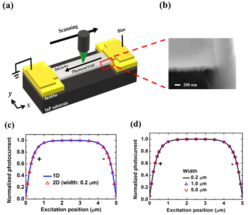
Carrier transport was studied both numerically and experimentally using scanning photocurrent microscopy (SPCM) in two-dimensional (2D) transport structures, where the structure size in the third dimension is much smaller than the diffusion length and electrodes cover the whole terminal on both sides. The scanning photocurrent simulation results surprisingly showed almost identical profiles from structures with different widths. The simulation results indicate that the integrated carrier distribution in the 2D transport structures with finite width can be well described by a simple-exponential-decay function with the carrier decay length as the fitting parameter, just like in the 1D transport structures. Furthermore, our simulation results demonstrate that the scanning photocurrent profiles in the ohmic- or Schottky-contact three-dimensional (3D) transport structures with electrodes covering the whole terminal on both sides will reduce to those described by the corresponding 1D fitting formulae. Finally, experimental SPCM on a p-type InGaAs
air-bridge two-terminal thin-film device was carried out. This study allows us
to extract the minority carrier decay length and to obtain the mobility-lifetime
product which can be used to evaluate the performance of 2D carrier transport
devices. This work has been published in
Scientific Reports:
Yu‑Chien Wei, Cheng‑Hao Chu, and Ming‑Hua
Mao*, “Minority Carrier Decay Length Extraction from Scanning Photocurrent
Profiles in Two-Dimensional Carrier Transport Structures,”
Scientific Reports,
11, 21863, (2021).
|
|
|
Fig. 1. (a) Schematic of the SPCM setup in an InGaAs air-bridge two-terminal thin-film device. (b) SEM images for one side of the measured InGaAs air-bridge two-terminal thin-film device. (c) Scanning photocurrent profile of the 0.2 μm wide case compared with that of the 1D transport structure. (d) Scanning photocurrent profiles with different widths. |
|
|
| |
|
|
|
|
|
|
| |
|
|
|
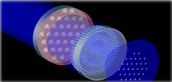
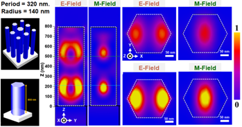
論文題目:可見光氮化鎵超穎透鏡之研究
姓名:陳孟忻
指導教授:林晃巖教授
| 摘要 |
|
超穎透鏡是超穎表面開發中最重要的應用之一。目前各式各樣的材料已被應用於製作超穎透鏡,使其在某些特定頻帶中達到高效率與低製造成本的需求。在這些材料中,考量材料的各項優點,尤其是在半導體製造的量產能力,寬能隙氮化鎵屬最具潛力的材料之一。在本論文中,氮化鎵被選為製造在可見光波段工作的高性能超穎透鏡的關鍵材料,而其超穎透鏡的設計原理乃基於幾何相位或傳播相位之概念。
幾何相位設計的超穎透鏡需要圓偏振平面波作為入射光,實驗結果在405、532與633奈米之可見光波長下,其繞射極限聚焦效率分別高達79%、84%和89%。另一方面,以傳播相位設計之超穎透鏡具偏振方向不敏感之特性,得以聚焦任意線性偏振方向之入射光。經實驗證明這些具偏振方向不敏感的超穎透鏡在405、532與633奈米之三個不同波長下,其繞射極限聚焦效率分別為93%、86%和92%。
在實際應用方面,本論文提出一個開創性的概念,即透過超穎透鏡檢測發光二極體的圖案化藍寶石基板。為了實施概念驗證,分別選擇不具有磊晶層以及具有磊晶層的市售圖案化藍寶石基板作為待檢測物,以執行超穎透鏡的檢測能力。透過適當選擇所需波長所設計的超穎透鏡,可以在圖中清楚地觀察到圖案化藍寶石基板中結構的頂點。
本研究為以寬能隙氮化鎵製作的超穎表面之應用展現了一道曙光。預計在不久的將來,超薄氮化鎵超穎透鏡將取代厚重的光學元件,成為未來光學的主流。
|
 |
|
圖一、透過超穎透鏡檢測圖案化藍寶石基板示意圖 |
|
 |
|
圖二、超穎透鏡排列方式以及單根柱對應之模擬電場磁場側視與俯視強度分布圖 |
|
|
|
|
|
|
|
| |
|
|
|
—
資料提供:影像顯示科技知識平台 (DTKP, Display Technology
Knowledge Platform) —
—
整理:林晃巖教授、吳思潔 —
受金屬有機框架保護的鈣鈦礦
高亮度發光體的發展是實現下一代高清顯示器的關鍵。負責視頻廣播技術標準的聯合國機構-國際電信單位(International Telecommunication Unit, ITU),提出1000至10000 cd m-2高亮度(BT.2020或Rec. 2020)用於超高清屏幕市場終端系統輸出。
鈣鈦礦發光二極體(Perovskite light-emitting diodes, PeLED)是未來顯示器的潛在候選者,因為它們與基於低成本的溶液製程具有兼容性,同時具有出色的色彩品質。 PeLED 提供最大的亮度水準達到104 cd m–2(參考文獻1, 2)的數量級,原則上滿足BT.2020的亮度表現,但沒有系統損耗的餘地。鈣鈦礦奈米晶體(Perovskite nanocrystals, PeNCs)是出色的發射器,因為它們具有高色彩純度,這源於窄的發射光譜,其半高全寬(FWHM)為20 nm。此外,通過控制成分,特別是鹵素含量,可以方便地調整PeNC發射的顏色。結果是,使用PeLED應該可以實現比傳統有機LED具有更寬色域的顯示器,傳統有機LED由於其振動耦合(vibronic coupling)而具有寬帶發射光譜。值得注意的是,鈣鈦礦奈米晶體LED也已實現,其操作效率超過20%(參考文獻2)。
然而,目前即使在100 cd m-2數量級的低亮度水準下運行時,PeLED的工作壽命通常也僅限於幾分鐘到幾小時,與BT.2020中的ITU最小值相差一個數量級。迄今為止,在低亮度級別,所量測到最佳工作時間達到數百小時(在500 cd m-2下大約為300小時)[3],同時更高的工作亮度下元件壽命呈現指數下降。主要問題常見於PeNCs在薄膜中本質上是不穩定的。PeNCs通常會降解為體相(bulk phase)。特別是在運行期間施加在器件上的電場的影響下,離子遷移占主導地位,這被視為主動器件條件下PeNC壽命短的最主要原因。因此,在主動LED中保持PeNC穩定使達到高亮度水準是實現BT.2020兼容性的主要挑戰。
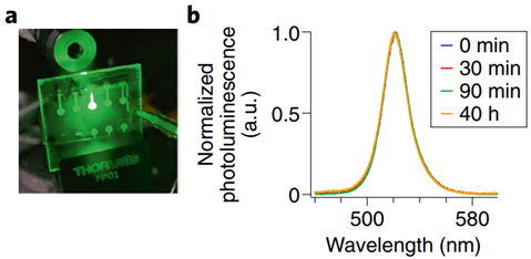
現在報導在Nature Photonics中,Tsai及其團隊使用金屬有機框架(metal–organic frameworks, MOF)來穩定發光薄膜中的PeNC[4]。結果是LED的電驅動活性層(圖1a)避免了離子遷移以及合併到體相的問題,同時提供了令人印象深刻的最大亮度水準超過105 cd m-2。
作者在介孔Pb-MOF矩陣結構中原位獲得了具有約8 nm和13 nm雙尺寸分佈的發射性甲基銨三溴化鉛 (MAPbBr3) 奈米晶體,該矩陣結構預先建構為基板上的三維(3D)網絡化薄膜。最終轉換的Pe-MOF結構在其產生的LED運行期間和之後持續顯示一個FWHM約為20 nm的出光發射(圖1b)。這種MOF穩定的MAPbBr3奈米晶體LED 達到120,000 cd m-2 的亮度水準,這是綠色光譜範圍內的一個顯著水準。當在5000 cd m–2 的初始亮度水準(在 BT.2020 範圍內)下運行時,T50壽命(電激發光強度水準值減半的運行時間)量測為8.3個運行小時,並且在初始亮度150 cd m-2運行時間有40小時。在設備運行之後,PeNC 被證明完全沒有離子遷移或任何降解(圖1b)。這一項成就是未來為BT.2020兼容壽命長且明亮顯示器生產MOF穩定的PeNC LED的一個重要里程碑。
|
|
|
圖1、MOF PeNC LED。 a. 運行中MOF穩定的PeNC LED。 b. 以電驅動LED數小時後PeNC的光激發光光譜。發現發射光譜在發射峰值和光譜寬度上都沒有變化。 |
在尋求穩定的PeNC的過程中,必須防止離子遷移以實現長期穩定性,因為它會導致元件性能不可恢復的衰退。為了穩定PeNC,各種不同的策略被報導,包括使用添加劑進行鈍化、摻雜、配體工程(ligand engineering)和調整奈米晶體的核殼結構。 MOFs以前也被用作PeNCs的宿主矩陣結構,以提高其穩定性[5-9]。然而,這些早期研究的重點並不是電驅動的發光薄膜。這裡的技術挑戰是沉積均勻的電激發光薄膜以製造優質LED,同時保持足夠的導電性以有效地注入電荷。關鍵的控制參數是前體(precursor)的濃度和薄膜厚度,以平衡薄膜中形成的發射中心的數量和將電荷均勻注入薄膜的能力。Tsai等人將Pe-MOF結構優化至210 nm的膜厚。
製作均勻的發光薄膜對於製造高性能LED非常重要。要建構均勻的發射層,首先需要構建具有良好均勻性和覆蓋範圍的MOF網絡。MOF通常在有機溶劑中的溶解性較差,這阻礙了在薄膜上形成均勻的3D MOF結構。為了解決這個問題,會加入酸來仔細調整pH值,將MOF溶解成透明溶液進行旋塗(旋轉塗佈,spin-coat)。然後旋塗Pb-MOF薄膜以構建3D介孔結構,將Pb與羧基(carboxylic)有機橋連接起來。得到的MOF薄膜清晰且具反光特性,說明薄膜粗糙度降低。接著通過旋塗引入含有前體的鹵化物鹽(halide salts),以將Pb-MOF轉化為Pe-MOF。使用這種連續的兩步沉積技術,可以為Pe-MOF轉換機制找到最佳操作窗口,以產生高效性且均勻的發射。
雖然PeNCs壽命短的主要原因被認為是在運行中的元件上施加的電場影響下觸發的離子遷移,但仍有其他機制會導致設備性能衰減,包括界面或電化學反應,以及外部因素(濕度和溫度)[10,11]。儘管Tsai等人發現,在主動元件運作致使老化後,MOF保護的PeNCs的光致發光出射峰值和FWHM沒有受到影響,LED仍然表現出衰退的性能,這說明存在額外的老化機制。作者認為該元件可能受到界面極化的影響。儘管明確地阻止了離子遷移,但界面可能會遭受界面極化,說明需要進一步的設備工程設計。
實現105 cd m-2以上的最大亮度是Tsai等人目前工作中記錄的一個重要的里程碑。這是非常出色的且展現出在高亮度的情況下進一步提高器件壽命的希望。當然要將中高亮度級別的設備壽命提高到10000個工作小時以上還有很長的路要走。然而必須注意的是,有機LED(OLED)在20年內達到了所需的使用壽命水平。PeLED研究界在這麼短的時間內達到了令人矚目的進展,對於我們在未來追求中高亮度BT.2020兼容顯示器的長期穩定性給予很多的希望。
|
參考資料: |
Vassili Fedotov, “Metal–organic frameworks protect perovskite,”
Nature Photonics volume
15, pages796–797 (2021)
https://doi.org/10.1038/s41566-021-00898-5
DOI:s41566-021-00898-5
|
|
參考文獻: |
[1] Yan, F. et al.
Nano Lett. 18, 3157–3164 (2018)
[2] Kim, Y.-H. et al.
Nat. Photon. 15, 148–155 (2021)
[3] Li, H. et al.
Adv. Mater. 33, 2008820 (2021)
[4] Tsai, H. et al. Nat. Photon. https://doi.org/10.1038/10.1038/s41566-021-00857-0 (2021)
[5] Zhang, C. et al. Nat. Commun.
8, 1138 (2017)
[6] Zhang, Q. et al. J. Solid State Chem. 272, 221–226 (2019)
[7] He, H. et al. Adv. Mater. 31, 1806897 (2019)
[8] Hou, J. et al. Angew. Chem. Int. Ed. 59, 19434–19449 (2020)
[9] Zhang, C. et al. Angew. Chem. Int. Ed. 60, 7488–7501 (2021)
[10] Yan, F. & Demir, H. V. Nanoscale 11,
11402–11412 (2019)
[11] Dey, A. et al. ACS Nano 15, 10775–10981 (2021)
|
|
|
|
|
|
|
|
|
|
|
|
|
|
|
|
|
|
|
|
|
|
|
 |
|
 |
|
|
|