|
|
 |
| |
发行人:黄建璋所长 编辑委员:曾雪峰教授 主编:林筱文 发行日期:2019.09.30 |
| |
|
 |
~
光电所参与欧盟
European Master of Science in Photonics (EMSP)
硕士双学位计划
系列报导 ~
【之八】
撰文:光电所硕士班
黄郁庭
相信大家从小就听过学校安排的无数演讲,而在我国中时我记得有位讲者和我们说:「今天我说的你全部都可以忘记,但请记住这句话,一定要出国念书看看。」这句话让我从当时起就想着,以后有机会的话,我也想去看看国外的世界,并体验当地的生活。
所以大家不妨出国前好好想一下,自己出国的动力是什么,以及要预先做好的准备。如果你出国是为了体验国外的风土民情,那么选择当交换学生相较之下课业压力轻松很多,有更多时间可以安排休闲娱乐。因为EMSP的学分我觉得要求很扎实,要在有限的时间内修课和写论文,并挪出时间去旅游其实不是容易的事情。但相对的,如果你想要拿取国外的硕士学位,用来帮助自己的就业,这就是很好的途径。
有一个能被承认的国外学历,对于将来无论在台湾或是国外的就业,都有一定程度的帮助。老实说我觉得在国外的论文题目内容并没有非常重要,比较要紧的是你在截然不同的环境下所学到的态度,而且我觉得这是当交换学生无法体会到的。在比利时的实验室里面,他们已经将研究生视为工作伙伴,所以会对你有比较高的标准与要求,犯错的宽容度也低很多。
除了在研究室外,和外国朋友相处也是某种文化刺激,像他们的教育制度和台湾相差甚大。我们从小就不断补习,接受填鸭式教育就为了进入好大学,许多人念大学却不知道自己想要什么,进而开始松懈;但比利时的教育是渐进式的,小学生下午两、三点就回家了,因此许多人会去参加俱乐部,像是踢足球、或学音乐,也有人骑马、玩童军,这点让我很羡慕。而他们直到大学课业压力才加重,因此反而同学都很认真,不太会逃课。
出国前我的人生规划很简单,找一间稳定的科技公司做到老,但现在的我在一间比利时外商上班,反而觉得不太习惯封闭的台商环境。说实话,人都有惰性且惯于安逸,往往在一个貌似还可以、得过且过的环境就容易陷下去,而我也是个很懒惰的人。不过出国后才发现世界很大,如果没有多接触到其它东西实在太可惜了!我觉得在国外求学这段岁月,给了我很大的勇气跳脱舒适圈,回首过去,依然不后悔自己的决定。
因为现在在比利时外商上班,顺便分享一下他们的文化,基本上办公室的工作强度蛮强的,但随时都可以跟同事或老板聊天,没有很明显的上下阶级,总之大家不是在埋首工作、开会,不然就是在聊天,基本上不会看到有人耍废偷逛网拍或是玩手机之类的行为,我个人是很赞同利用聊天来纾压这种行为,社交沟通手腕在公司非常重要,总而言之是非常不同的经验!【全文完】
|
 |
|
|
|
|
|
|
|
|
|
 |
|
| |
|
|
|
High Efficiency Laser Phosphor Lighting with Diffractive Optical Elements design for Beam Shaping
Professor Hoang-Yan Lin
Graduate Institute of Photonics and
Optoelectronics, National Taiwan University
台湾大学光电所 林晃岩教授
The ways for creating an efficient white light source are developed with challenges since several years ago. In solid-state lighting (SSL), laser diodes (LDs) offer a better efficiency at high power density applications compared to other lighting sources, such as, light emitting diode and organic light emitting devices. Therefore, the hot spot on phosphor plate which is produced by laser beam, critically influence the performance of laser phosphor lighting systems. Diffractive optical element (DOE) was introduced to homogenize the optical beam from LDs. Design of a DOE for beam shaping with uniform illumination has been widely employed for several applications, such as, laser cutting, laser drilling, and material ablation, etc.
In such uniform illumination processing, strong zero-order patterns frequently arise owing to the manufacturing error, which drastically reduces the uniformity of the diffraction pattern. Some methods for zero-order suppression have been reported, e.g., adjusting the amplitude and phase profiles by using a spatial light modulator (SLM) and using an off-axis system or additional elements. Estimation of the manufacturing error is indispensable for numerically calculating the phase profile of transmission functions of DOEs. By taking a simulated algorithm of laser beam shaping, the optical properties for the laser phosphor lighting system are improved with a beam shaping DOE.
The method we propose in this paper provides a high-power conversion efficiency for high power density laser lighting system. This approach might be beneficial for enhancing the lifetime and efficiency of the phosphor plate, which are hampered by the thermal issue due to hot spot from laser focusing, and improving the performance of laser phosphor lighting systems.
|
|
|
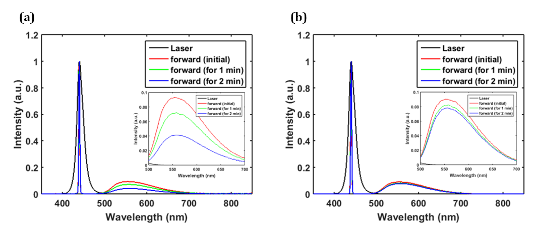
Fig. 1.Radiation spectra of laser phosphor lighting system with laser optical power of 2W (a) without DOE beam shaping (b) with DOE beam shaping. |
Ref. Min-Chian Wu, Yao Lee, Hoang Yan Lin, Chih-Hsuan Tsuei, Chih-Sheng Jao, Kuo-Hsiang Chien, High Efficiency Laser Phosphor Lighting with Diffractive Optical Elements design for Beam Shaping, SID 2019.
A New Analytic Formula for Minority Carrier Decay Length Extraction from Scanning Photocurrent Profiles in Ohmic-Contact Nanowire Devices
Professor Ming-Hua Mao’s
Laboratory
Graduate Institute of Photonics and
Optoelectronics, National Taiwan University
台湾大学光电所 毛明华教授
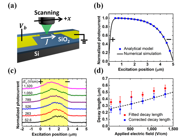
Spatially resolved current measurements such as scanning photocurrent microscopy (SPCM) as shown in Fig. 1(a) have been extensively applied to investigate carrier transport properties in semiconductor nanowires. In this work, we derive an analytic formula for scanning photocurrent profiles in widely used ohmic-contact nanowire devices where the common assumption of carrier diffusion dominance is invalid. Under uniform applied electric fields, weak optical excitation, and the influence of photo-carrier-induced electric field, the scanning photocurrent profile and the carrier spatial distribution strikingly do not share the same functional form. Instead, a surprising new analytic relation between the scanning photocurrent profile and the minority carrier decay length was established. Figure 1(b) shows the calculated scanning photocurrent profiles using analytical model and numerical simulation. The analytic formula is applied in SPCM experiments for an n-InAs nanowire, where electric-field-dependent decay length is found as shown in Fig. 1(c,d).This analytic formula provides a new fitting method for SPCM profiles to correctly determine the minority carrier decay length, which allows us to quantitatively evaluate the performance of nanowire-based devices. This work has been published: Chu, C.-H., Mao, M.-H., Yang, C.-W. and Lin, H.-H. ,Scientific Reports
9,
9426, (2019). doi:10.1038/s41598-019-46020-2
|
|
|
Fig. 1. (a) Schematic of a typical SPCM setup. (b) Calculated scanning photocurrent profiles using analytical model and numerical simulation. (c) Measured scanning photocurrent profiles with varied applied electric field. (d) The fitted and corrected hole decay lengths from the measured scanning photocurrent profiles as a function of the applied electric field. |
|
|
| |
|
|
|
|
|
|
| |
|
|
|
论文题目:以广义高斯常数使用于深紫外光学微影之成像与照明系统设计
姓名:萧立人 指导教授:林晃岩教授
| 摘要 |
|
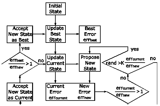
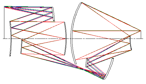
此研究的主要目的为开发及系统化极紫外光波段之光刻机之成像及照明系统的设计。光刻为一系列颇复杂的流程的组合。其中,最为关键的部分之一为曝光这一步骤。曝光机的成像质量,于其成品的制程密度与分辨率甚至于此制成的生产效率中间,存在直接的影响与关系。然而,曝光机之光学系统特性,及其参数之间,存在着许多复杂且繁琐之关系,导致于此光学系统不易分系,也不易设计。因此,此研究最为核心的目的,为研究及开发某一系统化之分析方法,以达到简化此光学系统之设计之目的。此研究核心之关键,为将广义高斯常数应用于光刻机之分析及设计上。通过广义高斯常数,众多复杂且繁琐之光学特性及光学系统之间之联系能以之表达及简化,而将所有关系结合并简化后,从中所导出之数学关系式可用于与商用光学设计软件之结合,以达到帮助分析及设计简化。图一为将之简化后所得之简易MonteCarlo优化算法。广义高斯常数之最初用途为变焦光学系统之分析及设计,其中通常有复数多件光学组件所组成之组合,及其为配合不同使用状况而改变位置及光学特性。而将之强大分析能力应用于极紫外光刻机之分析及设计为此研究之重要关键之一。图二为此研究之成果之一为某一 0.4 数值孔径之极紫外光刻机之反射式成像光学系统之分析与设计,以及其照明光学系统之分析与设计。
|
|
|
图一 |
|
|
|
图二 |
|
|
|
|
|
|
|
|
| |
|
|
|
— 资料提供:影像显示科技知识平台 (DTKP, Display Technology
Knowledge Platform) —
—
整理:林晃岩教授、吴昕妤 —
混沌的启发
混沌控制理论可以为同步加速器提供新的运行方式的机会,并提高稳定性和强度。这是来自里尔大学的法国科学家团队和巴黎附近的SOLEIL同步加速器系统机构(如图一)的发现。Clement Evain及其同事报告说,20世纪90年代由马里兰大学的Edward Ott,Celso Grebogi和James Yorke开发的混沌控制理论可用以稳定在本质上不稳定的兆赫兹同步辐射(Nat. Phys., https:// doi .org / 10.1038 / s41567-019-0488-6; 2019)。
|
|
|
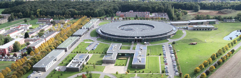
图一、SOLEIL同步加速器系统 |
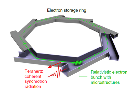
同步加速器是大规模的光源,利用在储存环(如图二)中循环的相对论电子束发出的辐射。它们的高亮度,短脉冲持续时间和可调谐性质(光子发射能量可以从兆赫兹频率到硬X射线),使它们成为生物学,材料科学和物理学研究中非常有用的电磁辐射源。
|
|
|
图二、同步加速器设施的的储存环与辐射示意图 |
多年来已经知道,电子电荷密度的不稳定微结构模式,可以在储存环内自发形成并且导致兆赫兹发射的瞬时突发,其比一般时强大了好几个数量级。然而,这些微结构所引起的不规则性和不稳定性使得它们不利于实际应用。
法国团队的创新之处在于他们已经证明,受混沌控制启发的反馈方案可用于稳定这些微结构及其兆赫兹发射,从而使系统能够在其它不稳定的解决方案中运行。该团队使用快速测辐射热计(1μs响应时间)来测量SOLEIL发射的同调兆赫兹辐射功率的波动。然后计算用于调制注入到SOLEIL的加速腔之一中的辐射频率波的振幅的合适控制信号,并用于修改电子束长度,并减轻爆破行为。结果是,在几毫秒内,兆赫兹功率得以稳定。发现辐射频率信号强度小于0.3%的修改足以将兆赫兹输出的波动减小40dB以上。
|
参考资料: |
[1] Oliver Graydon, “Inspired by chaos,”
Nature Photonics 13, 375 (2019)
https://www.nature.com/articles/s41566-019-0455-x
DOI: 10.1038/s41566-019-0455-x
[2] C. Evain, C. Szwaj, E. Roussel, J. Rodriguez, M. Le Parquier, M.-A. Tordeux, F. Ribeiro, M. Labat, N. Hubert, J.-B. Brubach, P. Roy & S. Bielawski, “Stable coherent terahertz synchrotron radiation from controlled relativistic electron bunches,”
Nature Physics 15, 635–639 (2019)
https://www.nature.com/articles/s41567-019-0488-6
DOI: 10.1038/s41567-019-0488-6
|
| |
|
|
|
|
|
|
|
|
|
|
|
|
|
|
|
|
 |
|
 |
|