|
|
 |
| |
發行人:林恭如所長 編輯委員:李翔傑教授 主編:林筱文 發行日期:2018.09.30 |
| |
|
 |
|
 本所曾雪峰教授獲選為「教育部107年度生命教育績優人員」,特此恭賀!
 本所林本堅特聘研究講座教授因持續擴展奈米級積體電路製造,榮獲2018年「未來科學大獎」之「數學與計算機科學」獎項,特此恭賀! 本所林本堅特聘研究講座教授因持續擴展奈米級積體電路製造,榮獲2018年「未來科學大獎」之「數學與計算機科學」獎項,特此恭賀!
未來科學大獎目前設置「生命科學」、「物質科學」和「數學與計算機科學」三大獎項,單項獎金100萬美元。要求其工作產生巨大國際影響,具有原創性、長期重要性或經過時間考驗,並主要在大中華地區完成。
相關報導網頁連結:
http://www.futureprize.org/
https://udn.com/news/story/7240/3356731
|
|
 |
|
 |
|
| |
|
|
|
|
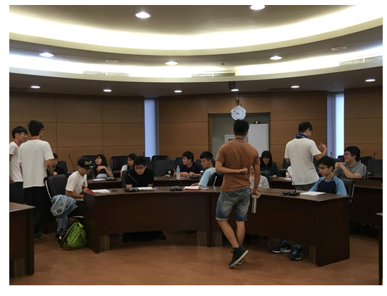
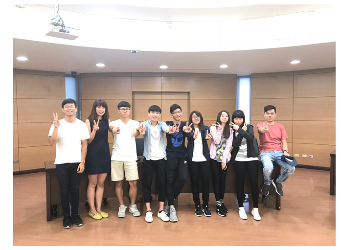
~ 2018 暑期大學生光電營 花絮報導 ~
(時間:107年8月16日至17日;地點:臺灣大學博理館
)
花絮整理:所學會會長郭勝文
每年暑假,光電所會邀請各大學的學弟妹參加光電營的活動,今年也不例外。學弟妹來自四面八方,有的家就在台北,也有人住屏東為了來參加光電營而北上,令我們驚喜萬分,謝謝你們願意花暑假放假的時間來報名參加我們的營隊。
活動一開始時,我們將學弟妹分組,約6至8人為一組,接著我們利用一些時間認識彼此,了解他們為什麼會想來參加這個營隊,大部分的回答皆是想來看看光電所都在做些什麼或是暑假不知道要做什麼,而特別讓我們感到驚喜的回答則是未來想來臺大光電所就讀。我們也介紹自己,包含平常的生活和實驗的部分。
|
 |
 |
|
圖一、隊員與隊輔互動 |
圖二、隊員與隊輔互動 |
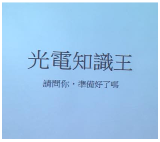
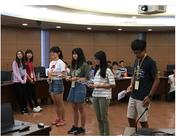
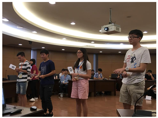
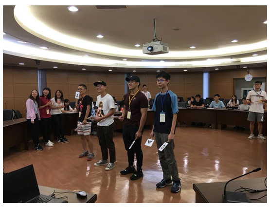
之後為了瞭解彼此與增進隊員感情,我們準備名為「光電知識王」的活動讓他們透過競賽來互動,並且累積積分,最後積分多的可以獲得光電所準備的精美禮物,利用這個活動可以讓我們更了解小隊員的個性,每位隊員都為了自己隊上的榮耀而努力著。
|
 |
 |
|
圖三、光電知識王投影封面 |
圖四、光電知識王實戰情形 |
|
 |
 |
|
圖五、光電知識王實戰情形 |
圖六、光電知識王實戰情形 |
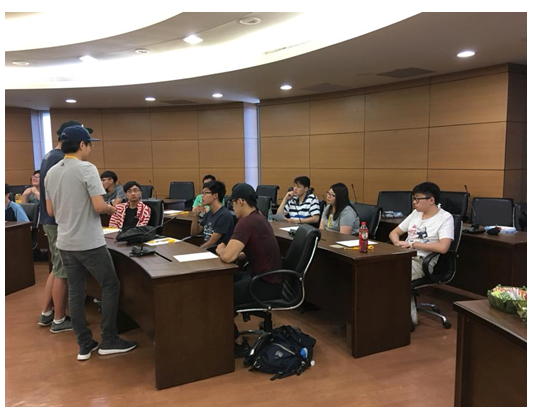
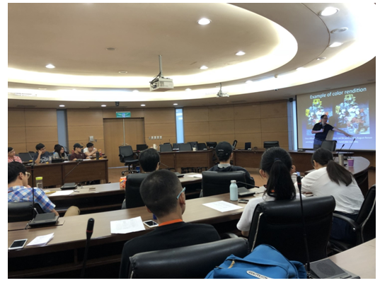
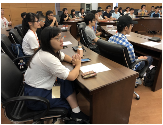
接著是課程的部分,我們請到所上教授或是博士班學長來替我們講授一些關於光電的知識,透過專業的報告介紹關於光電的知識與分享光電產業的發展,每位學弟妹都聽得很專注,從教授或是學長的分享中獲得專業知識,也許學弟妹不是立刻都能融會貫通,但或多或少從中得到一些前輩們的經驗,可以對未來預先規劃,收穫一定能讓學弟妹不虛此行。
|
 |
 |
|
圖七、課程講授(授課教師黃建璋教授) |
圖八、認真聽課的學弟妹 |
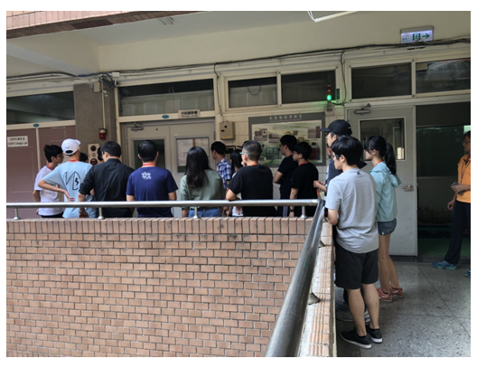
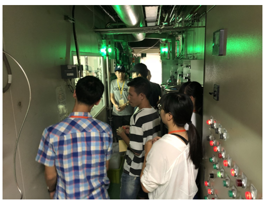
課程中我們還有參觀無塵室與E-Beam實驗室的安排,雖然無法讓大家動手操作,不過我們藉由介紹的方式和親眼目睹儀器,讓大家有深刻的印象及初步瞭解,當中非常謝謝無塵室的廠務翁菲萍小姐和管傑雄老師實驗室的幫助。
|
 |
 |
|
圖九、參觀無塵室 |
圖十、參觀E-Beam實驗室 |
最後是頒發證書的時刻,很感謝全程參與的學弟妹,讓光電所舉辦的活動變得值得,當拿到證書時每個人的臉上都充滿了笑容,相信你們對於這次的營隊都感到開心且滿足,不只是初步瞭解光電所、光電知識,最重要的是你們已經開始在規劃自己的未來了。雖然只有短短的兩天,經過短暫的相遇,我們期待著你們未來的大放異彩。這次活動非常感謝所辦與所上的教授同學,也很謝謝所學會的夥伴,謝謝大家。
|
|
|
圖十一、所學會的夥伴 |
|
|
|
|
|
|
|
|
|
|
| |
|
|
|
Investigation of Streptavidin-Ligand Biochemical Interactions by IGZO Thin Film Transistors Integrated with Microfluidic Channels
Professor Jian-Jang Huang's laboratory
Graduate Institute of Photonics and
Optoelectronics, National Taiwan University
臺灣大學光電所 黃建璋教授
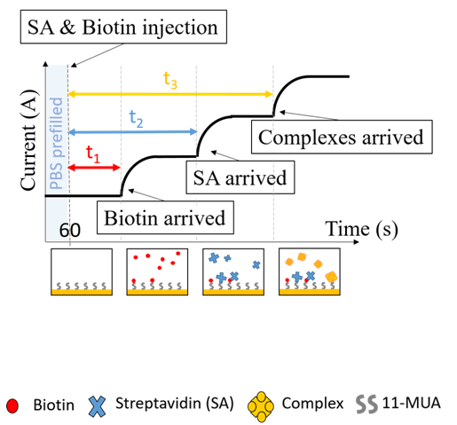
This is a joint research work between Prof. Y.-H. Lo from UCSD and Prof. J.-J. Huang from GIPO NTU. In this work, we demonstrate an IGZO TFT-based biosensor integrated with a microfluidic channel to monitor biochemical reactions between proteins and small molecules. The target biomaterials are applied to a Y-shaped microfluidic chamber while the reactant signal is readout by the TFT. Using Biotin-Streptavidin reaction as an example, the specific diffusion time of biotin, streptavidin, or streptavidin-biotin complex across the fluidic channel are benchmarked. By intentionally delaying the application of one specie to another, one can study properties of biochemical reactions, such as excess and exhaust conditions of the reactants, and the formation of the products while diffusing in the channel. The proposed TFT sensor provides an excellent platform in understanding the biochemical functions for the advance of biological science and drug discovery.
Ref: This work was published in “Sensors and Actuators B: Chemical. 262. 10.1016/j.snb.2018.01.177”
|

|
|
Figure 1. (a) The cross section of the IGZO-TFT (b) Schematic diagram of a reusable TFT biosensor. The TFT and microfluidic channel were fabricated separately and then connected together by a bond wire. The cross linkers were applied on the surface of ROI. |
|
|
|
Figure 2. Scenarios of drain current responses when the biotin and streptavidin are applied to the fluidic channel. Using the transient response of drain currents, our system is able to detect the complete and incomplete bioreactions. The control measurement was also conducted to verify the reaction between ligands and proteins. |
High-Performance Vertically-Stacked Complementary Inverter Composed of Oxide Thin-Film Transistors
Professor I-Chun Cheng
Graduate Institute of Photonics and
Optoelectronics, National Taiwan University
臺灣大學光電所 陳奕君教授
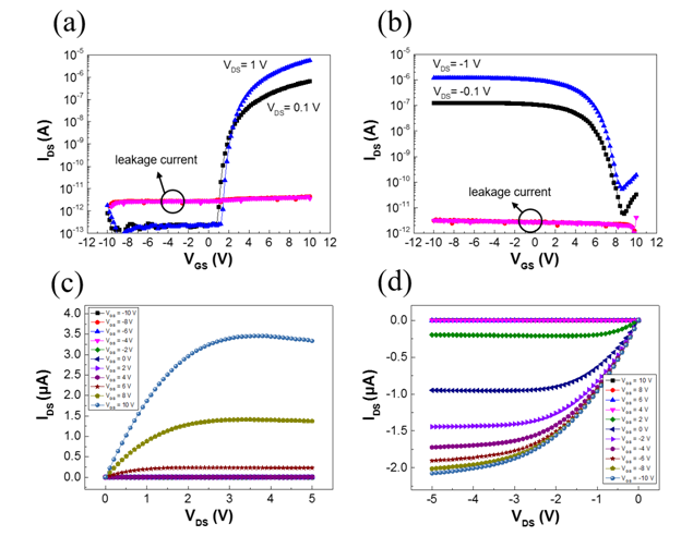
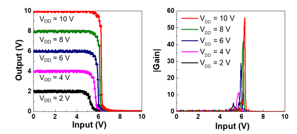
Complementary thin-film transistor (TFT) inverters are the fundamental building blocks for versatile thin-film logic circuits. They possess several desirable features, such as low static power consumption and high density circuit integration. Complementary inverters implemented in a vertically-stacked structure offer an additional advantage, small footprint, in comparison with their coplanar counterparts. Oxide semiconductors are promising candidate channel materials for TFT applications because they have relatively high carrier mobilities and can be processed at low temperatures. In this research, we report an on-glass high-performance vertically-stacked complementary inverter based on oxide TFTs. It is composed of a bottom-gate n-type ZnO TFT stacking on a top-gate p-type SnO TFT. Both active layers were deposited by a low-temperature rf-sputtering technique. Fig. 1 shows the transfer and output characteristics of both the ZnO and SnO TFTs. The ZnO TFT exhibits a threshold voltage of 5.1 V, field-effect mobility of 2.5 cm2/V-s, subthreshold swing of 1.8 V/decade, and on/off current ratio of 2.4х107. The corresponding values for the SnO TFT are 6.2 V, 0.35 cm2/V-s, 0.9 V/decade, and 2.2х104. Fig. 2 shows the static voltage transfer characteristics and gain curves of the vertically-stacked complementary oxide-TFT-based inverter with a geometric aspect ratio of 5 at supplied voltages ranging from 2 to 10 V. A high voltage gain of 56 V/V at a supply voltage of 10 V is achieved. The result demonstrates the feasibility of realizing oxide-TFT based complementary circuits with high-density integration.
|
|
|
Fig. 1 (a)(b) Transfer and (c)(d) output characteristics of the bottom-gate n-channel ZnO TFT and top-gate p-channel SnO TFT. The channel dimensions are W/L = 40 μm/ 20 μm. |
|
|
|
Fig. 2 (a) Static voltage transfer characteristics and (b) gain curves of the vertically-stacked complementary TFT inverter with a geometric aspect ratio of 5 at supply voltages ranging from 2 V to 10 V. |
|
|
| |
|
|
|
|
|
|
| |
|
|
|
論文題目:以水溶液摻雜法製備超低接觸電阻石墨烯場效電晶體
姓名:黃國祐 指導教授:吳志毅教授
| 摘要 |
|
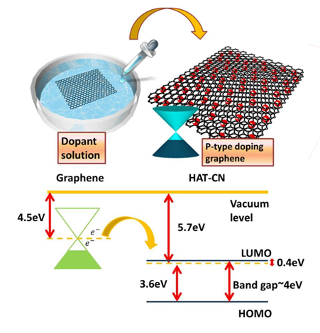
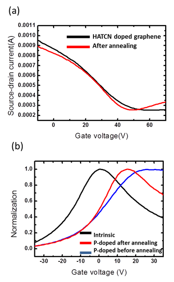
接觸電阻對於石墨烯(graphene)元件的效能具有關鍵性的影響,本研究使用了一種無須高分子輔助的轉印手法,以確保石墨烯樣品表面完全清潔,進而降低石墨烯與金屬電極間之接觸電阻以及提升元件效能,並且搭配使用真空退火(vacuum annealing)以及水溶液高分子摻雜改良石墨烯元件與金屬電極之接觸特性。進一步發現,使用HAT-CN聚合物摻雜過後之石墨烯,其功函數具有大幅度提升並形成P型石墨烯(機制如圖一所示)。其接觸電阻可大幅降低至36 Ω•µm,而在經過低溫熱退火後則可降低至24 Ω•µm。本實驗以改良後之超低接觸電阻石墨烯場效電晶體(Graphene Field-Effect transistors; GFETs)進行電性量測後,可發現元件之載子遷移率具有大幅度的提升,搭配ODTS自組裝層(Self-Assemble
Monolayer; SAM)所修飾過之基板後便可得到電洞遷移率約為14400 cm2
V−1 s−1之石墨烯電晶體。而經由水溶液P型摻雜修飾過之石墨烯雖然會因為庫倫散射之原因使其載子遷移率下降,但由於可大幅大改善石墨烯與金屬間之接觸電阻,因此載子遷移率亦可達到約5173
cm2 V−1 s−1
,(如圖二所示)仍舊是非常具有競爭力之效能。本研究設計了降低石墨烯與金屬電極間之接觸電阻之結構與方法,除了提升石墨烯應用於各式元件之價值外,更可進一步搭配其他二維材料,使得二維材料的研究與應用能夠更廣更全面,對於科學以及工業界的發展可以帶來更進一步的幫助。
 |
|
圖一、水溶液摻雜示意圖及HAT-CN摻雜機制 |
|
 |
|
圖二、(a) 摻雜HAT-CN後之石墨烯場效電晶體IV曲線 (b) 本質與摻雜後電晶體之電性曲線比較可發現狄拉克點(Dirac point)有明顯位移 |
|
|
|
|
|
|
|
|
| |
|
|
|
—
資料提供:影像顯示科技知識平台 (DTKP, Display Technology
Knowledge Platform) —
—
整理:林晃巖教授、孟慶棠 —
紙上電子
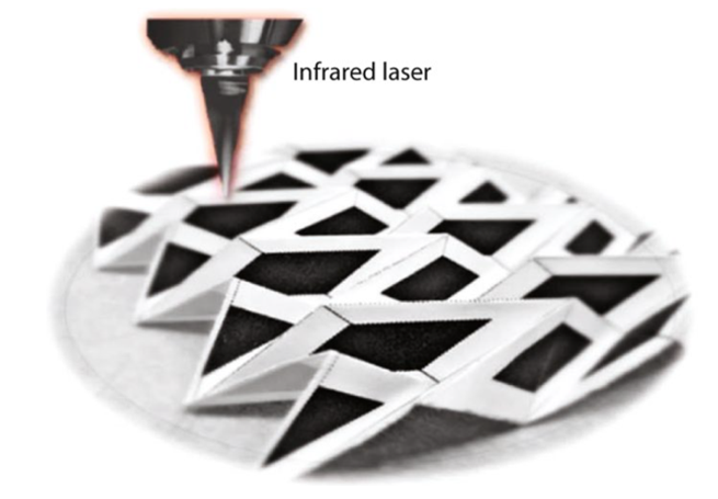
以雷射為基礎的製造方式可支援從大型汽車零件到微小生醫支架的各種元件的製造。現在,來自美國和中國的科學家的研究展示,雷射可以幫助實現3D可折疊式的紙上電子,如圖一所示。來自加州大學柏克萊分校、清華柏克萊深圳研究所和美國陸軍紅石兵工廠研究中心的Xining Zang和同事開發了一種直寫式雷射造型程序,其可在紙上產生導電性碳化鉬-石墨烯(MCG)區域(Adv.Mater.
https://doi.org/10.1002/adma.201800062; 2018)。
 |
|
圖一、在紙基板上(白色區域)利用雷射直接寫入MCG造型程序(黑色區域)之後,所製造摺紙結構的光學照片 |
雷射寫入可以在有環境光的條件下進行。首先將含有Mo5+離子的凝膠油墨噴灑於紙上,然後利用10.6-μm CO2雷射的光束以所需的造型掃描於紙上,用以產生可用作電極或電通道的黑色導電區域。寫入雷射的功率為2W;寫入速度為200mm s–1。樣品的拉曼與X光繞射結果顯示了雷射寫入後Mo3C2與石墨烯的存在。雷射照射區域的薄層電阻為每平方51.3Ω,此低於使用水溶性聚合物,其代替凝膠時所獲得的薄層電阻。有趣的是,較厚的紙可以吸收和保持更多的墨水,因此可以在雷射寫入後得到較低的薄層電阻。
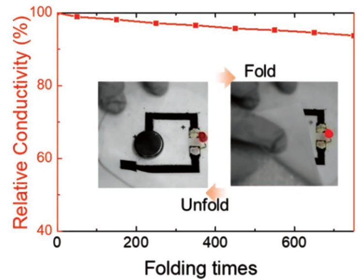
商業性複印紙具有良好的機械性強度和較低的薄層電阻。測試結果表示,紙上的MCG區域對於重複180°折疊性操作具有彈性。前50次折疊性操作通常導致電導率降低13%,但在隨後的750次循環中電導率維持小於5%的衰減,如圖二所示。此團隊預見導電紙無數潛在的應用,其包括電化學離子偵測器和氣體感測器、3D壓電發電機和超級電容器電極。
 |
|
圖二、記錄180°機械式折疊試驗的750次循環中,由MCG複合材料所製成的電性連接器的相對電導率。其中插圖為使用機械式折疊和接觸由MCG複合材料所製成的電極作為電性開關來開啟或關閉紅色發光二極體
。 |
|
參考資料: |
[1] Noriaki Horiuchi, “Paper electronics,”
Nature Photonics 12, 381 (2018)
https://www.nature.com/articles/s41566-018-0206-4
DOI: 10.1038/s41566-018-0206-4
[2] Xining Zang,* Caiwei Shen, Yao Chu, Buxuan Li, Minsong Wei, Junwen Zhong,
Mohan Sanghadasa, and Liwei Lin*, “Laser-Induced Molybdenum Carbide–Graphene Composites for 3D Foldable Paper Electronics,”
Adv. Mater., 30, 1800062 (2018)
https://onlinelibrary.wiley.com/doi/abs/10.1002/adma.201800062
DOI: 10.1002/adma.201800062
|
| |
|
|
|
|
|
|
|
|
|
|
|
|
|
|
|
|
 |
|
 |
|