|
|
 |
| |
发行人:林恭如所长 编辑委员:吴肇欣教授 主编:林筱文 发行日期:2017.10.30 |
| |
|
 |
|
 本所孙启光教授荣获教育部「第61届学术奖—工程及应用科学类科」,特此恭贺!
 本所曾雪峰教授荣获教育部「2017年度友善校园奖—大专校院杰出导师」,特此恭贺!
林清富教授指导本所硕士生同学荣获「中国电机工程学会2017年度青年论文奖第三名」,特此恭贺!得奖名单如下:
|
获奖同学
|
指导教授 |
论文题目 |
|
郭柏村硕士生 |
林清富教授 |
利用三明治蒸镀法制备平面异质接面型钙钛矿太阳能电池 |
|
|
 |
|
 |
|
| |
|
|
|
|
~ 2017学年度光电所所学会会长自我介绍 ~
光电所的师长、所办同仁以及同学们大家好,我是2017学年度所学会会长郭胜文,将会在接下来的一年为大家服务。首先要谢谢上一届会长蔡瑞祥学长的引荐,在交接会长的过程中帮助我许多,我很荣幸能有机会接下这个职位,也谢谢所办小姐的帮忙与提醒,希望在这一年能好好经营所学会这个大家庭,延续学长姐们所传达的精神。
也许新生对于所学会不太熟悉,所以在这边向大家做个简单的说明,让大家对于所学会有个基本的了解。所学会是学生的代表,代替学生争取应有的权益,且所学会也会负责办一些活动让所上的大家有机会互相认识,彼此交流情感,拓展自己的交友圈。
主要的活动有两个,第一个是上学期的期末餐会,提供美食与表演让大家快乐地享受,让各位在研究之旅中,享有一个与所上同侪互动的午后时光,增添在研究所的美好回忆。接着,我们会在下学期举办一场球类竞赛,竞赛的目的不在于输赢,输赢只是比赛最后的结果,过程中以球会友、交流球技才是主要的目的。
研究所短短两年的时间,大家的生活几乎都在实验室里做研究,或是坐在教室看着黑板,体会字里行间的奥秘,这些确实重要,但人际交流也就渐渐疏远了,也许生活圈就局限在实验室里了。所学会的目的就是帮助大家藉由活动拉近彼此之间的关系,认识新朋友,透过交流互动后才发现原来我们这么近,人生犹如白驹过隙般稍纵即逝,若不能在这趟研究之旅中留下美好回忆,岂不是太可惜了吗?我们所学会非常欢迎你的加入,继续让这个温馨的家庭扩大再扩大,让大家的研究所生涯不只是研究,而是在回忆里增添回忆,使得积分起来到无限大。
所学会还有许多不足的地方,希望透过大家的参与让所学会变得更加完整。我是隶属于吴志毅老师实验室的硕班新生,欢迎各位如果有其它想法可以寄信至光电所学会信箱,或是欢迎到我们实验室聊聊,在此谢谢所办小姐们的帮助,也谢谢指导教授对我们的支持。最后就是诚挚地再邀请大家,不论是新生或旧生,欢迎你的加入,让所学会更加完整。
|
|
|
|
|
|
|
|
|
|
| |
|
|
|
Multi-Band Infrared Thermal Emitter with Selectable Polarization
Professor Si-Chen Lee’s laboratory
Graduate Institute of Photonics and
Optoelectronics, National Taiwan University
台湾大学光电所 李嗣涔教授
This study demonstrated a multi-band infrared thermal emitter featuring a narrow bandwidth emission and polarization characteristics, which is quite suitable to be applied to the non-dispersive infrared (NDIR) detection system. NDIR system has been widely used in monitoring the hazardous and harmful substances in the human living environment. The target molecules can be detected by measuring the transmission optical energy at specific wavelengths due to their particular molecular bond vibration, which is inversely proportional to the molecular concentration in the NDIR system. Because the biomolecules usually exhibit multiple absorption peaks in the infrared regions, the multi-wavelength infrared light source plays an indispensable role in the NDIR system. The device is constructed by embedding the metallic grating strips within the resonant cavity of a metal/dielectric/metal (MDM) structure, as shown in Fig. 1(a) and 1(b). This arrangement makes it possible to generate waveguide resonances with mutually orthogonal polarization, thereby providing an additional degree of freedom to vary the resonant wavelengths and polarizations in the medium infrared region. The measured reflection spectra and the finite-difference time-domain simulation indicated that the electric fields of the waveguide modes with two orthogonal polarizations are distributed in different regions of the cavity, as shown in Fig. 1(c) and (d). Resonant wavelengths in different polarizations can be adjusted by altering the period, the metallic line width, or the position of the embedded gold strips. The ratio of the full width at half maximum (FWHM) to the peak wavelength was achieved to be smaller than 0.035. This work has been published in AIP
Advances 7, 085122 (2017).
|
|
|
FIG. 1. (a) A photograph of the multi-band infrared thermal emitter with polarized waveguide modes. (b) Schematic diagrams of polarized waveguide thermal emitter. (c) The experimental and FDTD simulated reflection spectra in x- and y-polarizations. (d) The experimental thermal radiation spectra of the device in x- and y-polarizations. |
High-resolution Analysis of Leaky Modes in Surface Plasmon Stripe Waveguides
Professor Hung-chun Chang
Graduate Institute of Photonics and
Optoelectronics, National Taiwan University
台湾大学光电所 张宏钧教授
The surface plasmon polariton (SPP) existing at an interface between metal and dielectric material is a basic phenomenon in the area of “plasmonics” and has been a well-known wave mode particularly in the visible and infrared wavelength ranges. With the rapid progress of the plasmonics research in recent years, various SPP waveguides have also been proposed and investigated. Here, we report our recent studies of the stripe plasmonic waveguides with a gold stripe having a silica substrate. Such simple structure was one of the earlier studied SPP waveguides. Weeber
et al.
reported
their experimental measurement results of waveguide mode
characteristics of such structure in 2003 [Phys. Rev. B
68, 115401 (2003)]. Zia
et al. in 2005 [Phys. Rev. B
71, 165431 (2005)] presented finite-difference numerical analysis of the same waveguides, obtained their leaky and bound modes, and concluded that calculated leaky mode characteristics could be consistent with the observed SPP-propagation ones by Weeber
et al. Zia
et al. calculated the real and imaginary parts of the complex effective refractive indices,
neff’s, of the leaky, quasi-transverse-magnetic (quasi-TM) SPP modes for different stripe widths, where
neff is defined as
the modal propagation constant divided by the free-space wavenumber. We have
recently conducted high-resolution finite-element numerical analysis of the same
stripe waveguide using an in-house developed full-vector finite-element
imaginary-distance beam propagation method (FV-FE-ID-BPM) and discovered some
subtle mode-field characteristics in the leaky modes so that the
neff versus the stripe width curves appear to be of non-monotonic variation [H. H. Liu and H. C. Chang, J. Lightwave
Technol.
34,
pp. 2752–2757 (2016)]
|
|
|
Figure 1 Mode-field profiles of the TM1 mode of the stripe waveguide when the stripe width is 3.7
μm: (a) Re[Ex], (b) Re[Hx], (c) Re[Ey], (d) Re[Hy], (e) Re[Ez], and (f) Re[Hz]. |
Fig. 1 shows the magnitude profiles of the real parts of the six field-component phasors of the lowest TM1 mode for the stripe width of 3.7 μm (the gold stripe thickness is 55 nm). In each panel, the horizontal thin black line shows the boundary of the substrate, and the outline of the boundary of the stripe cross-section appears to be the thicker portion of the thin black line. In the analysis we used 638,347 unknowns for the computational domain of 8 μm x 11.5 μm size, which covers the right or left half of the waveguide cross-section making use of the structure symmetry. Such high spatial resolution and large coverage of the substrate region reveals the details of the leaky fields in the substrate including the interference feature. It is interesting to notice that the two stripe edges provide two sources for the propagating leaky fields. Note that
Hx (Fig. 1(b)) and
Ey (Fig. 1(c)) are the major field components. For further discussions, please refer to [J. Lightwave
Technol.
34,
pp. 2752–2757 (2016)].
|
|
| |
|
|
|
|
|
|
| |
|
| |
|
|
|
— 资料提供:影像显示科技知识平台 (DTKP, Display Technology
Knowledge Platform) —
—
整理:林晃岩教授、王子圣 —
涡旋式分拣机 (Vortex Sorter)
涡旋光束(optical vortex beam)可用于粒子处理、量子光学、通信及其它应用。在通信中,可以透过具有不同轨道角动量(orbital angular momentum)的空间重迭模态来增加(数据)传输量。这些模态可以透过各种庞大的方法,包括:空间光调制器或由计算器数值控制(CNC)路由器或相关铣削方法制作成的厘米级绕射组件去分离或解复用(demultiplexed)。然而,这些组件对于集成化应用(如用于光纤尖端)来说相对较大。
现在,来自以色列的Shlomi Lightman及其同事采用直接激光印刷技术制造了用于复用(multiplexing)和解复用(demultiplexing)光轨角动量状态的微米级结构。第一个示范使用了两个绕射相位组件,而第二个示范则展示了组合所需组件的集成化组件(如图一所示)。
 |
|
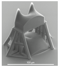
图一、扫描电子显微镜下组合模式分拣机的图。转换器和校正组件集成在玻璃基板上,需要相对大的柱体才能进行精确的对准。 |
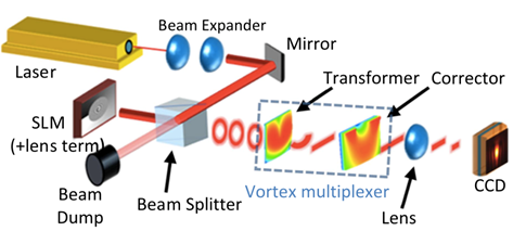
为了研究解复用性能,研究人员产生了不同的涡旋光束。他们对解复用能力进行了测试,但是基于对称性的考虑,当设备用作复用器时,预期的性能会相同。在CW(是指窄而明确的光谱辐射,亦即连续波)模式中使用具有690-1040 nm可调范围的Mai Tai钛蓝宝石振荡激光(Spectra-Physics, USA)。将仅具相位变化之反射式空间光调制器(PLUTO-NIR-011, HOLOEYE, USA) 编程为空间调制光束的相位,接着将光束聚焦到(解)复用器中的附加透镜项,如图二所示。一道焦距160 mm、数值孔径大小为0.01的高斯光束被聚焦到一个56 μm的光点大小(1∕e2),即,约比波长大50倍,因此实验装置完全是在近轴的近似之内。
 |
|
图二、用于测试涡旋复用器的光学设计示意图 |
研究团队使用商业3D直接激光写入系统印刷了波长在780 nm、而折射率为1.51的材料结构。印刷后,将该结构在显影剂中漂洗并用异丙醇进行清洗处理。间隔为60 μm之两个组件(转换器和校正器)的体积分别为60 × 60 × 32 μm3
和60 × 30 × 51.5 μm3。
在连续波模式中使用由钛蓝宝石激光照射的仅具相位之反射式空间光调制器产生涡旋光束,产生了从−3ħ到3ħ轨道角动量的光束。在展示中,光束会在每角度动量单位上被空间分离9.4 μm。在此系统中,拓墣电荷必须小于5,但这可以透过调整两个组件之间的尺寸来增加,作者声称系统可以处理10电荷的涡旋光束。研究团队调整了印刷过程去分析表面粗糙度对设备性能的影响。如预期的那样,平滑的表面会引起较少的旁瓣和串扰现象。
研究人员对690、790、890和990 nm的波长进行了重复的实验,并展示了主要局限性为光致抗蚀剂分散的300 nm的频宽。他们认为,透过设计的优化可以实现波长范围在300 nm 到2,000 nm之间的操作。 然而,超出该范围的话,聚合物将变得不透明而应当使用其它材料。
|
参考资料: |
1. David Pile, Vortex Sorter, Nature Photonics 11, 459 (2017)
DOI:10.1038/nphoton.2017.137
http://www.nature.com/nphoton/journal/v11/n8/full/nphoton.2017.137.html
|
|
2. Shlomi Lightman, Gilad Hurvitz, Raz Gvishi, and Ady Arie, Miniature wide-spectrum mode sorter for vortex beams produced by 3D laser printing, Optica 4, 605–610; 201
DOI:10.1364/OPTICA.4.000605
https://doi.org/10.1364/OPTICA.4.000605
|
|
|
|
|
|
|
|
|
|
|
|
|
|
|
|
 |
|
 |
|