|
|
 |
| |
發行人:林恭如所長 編輯委員:吳肇欣教授 主編:林筱文 發行日期:2014.07.20 |
| |
|
 |
Si and SiC quantum dots co-doped Si-rich SiC p-i-n
junction diode with enhanced blue-green light emission
Professor Gong-Ru Lin's
Laboratory
Graduate Institute of Photonics and
Optoelectronics, National Taiwan University
臺灣大學光電所 林恭如教授
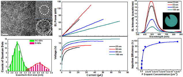
Si quantum dots (Si-QDs) and SiC quantum dots (SiC-QDs) co-doped Si-rich silicon carbide (SixC1-x) based p-i-n junction light-emitting diodes (LEDs) with blue-green light emission is demonstrated. By growing the SixC1-x with plasma-enhanced chemical vapor deposition (PECVD) at relatively low temperature, the turn-on voltage of Si-rich SixC1-x LEDs can be reduced to 6.1 V when thinning i-SixC1-x layer to 25 nm because of higher tunneling probability and lower series resistance. The electroluminescent (EL) power increases to 136 nW, however, which inversely attenuates due to the reduced SiC-QDs if the i-SixC1-x thickness further shrinks to 25 nm. The principle EL peak at 500 nm with narrower shape and blue-green emission pattern is attributed to the self-trapped excitons at surface states among SiC-QDs. The external quantum efficiency (EQE) of the Si-rich SixC1-x LEDs with i-SixC1-x thickness of 50 nm is up to
1.58×10⁻¹% with enhanced carrier tunneling probability. The carrier injection efficiency is enhanced to 46% by increasing the doping concentration to 1016
cm-3, leading to almost one order of magnitude improvement on the EQE of Si-rich SixC1-x LEDs.
|
 |
|
Figure Left: The TEM images (Upper) of the Si-rich SixC1-x films (Left) with co-doped SiC-QDs and Si-QDs in average sizes of 2.5 nm and 4.3 nm, respectively with the size distribution (Lower) of SiC-QDs and Si-QDs in the Si-rich SixC1-x film with the thickness of 50 nm. Middle: The I-V (Lower) and P-I (Upper) characteristics of the Si-rich SixC1-x p-i-n junction LEDs with different i-SiC thickness grown with the fluence ratio of 60%. Right: The EL spectra (Upper) of Si-rich SixC1-x p-i-n junction LEDs with the different i-SixC1-x thickness. Inset: the EL emission pattern. The carrier injection efficiency (Lower) of the Si-rich SixC1-x p-i-n junction LED as a function of n-type dopant concentration under fixed B2H6 doping concentration. |
Reference: Hung-Yu Tai, Chih-Hsien Cheng, and Gong-Ru Lin, “Blue-Green Light Emission from Si and SiC quantum dots co-doped Si-rich SiC p-i-n Junction Diode,”
IEEE J. Sel. Top. Quantum Electron., Vol. 20, Issue 4, 8200507, Jul.-Aug. 2014.
ITO-free
low-index transparent electrodes for enhancing
light out-coupling of organic light-emitting devices
Professor Chung-Chih Wu
Graduate Institute of Photonics and
Optoelectronics, National Taiwan University
臺灣大學光電所 吳忠幟教授
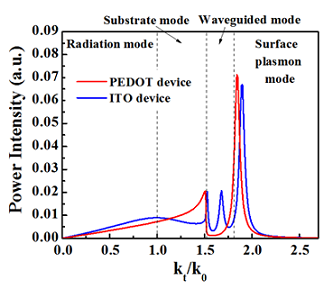
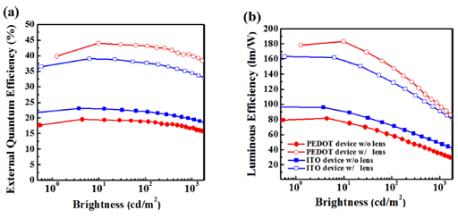
The transparent conductor indium tin oxide (ITO) has been widely used in organic light-emitting devices (OLEDs) and other organic/inorganic optoelectronics as the transparent electrode. ITO, however, is rather expensive and thus not cost-effective due to scarcity of the indium element on earth. ITO is also brittle and usually requires high-temperature processing, limiting its compatibility with flexible plastic substrates and thus its use for flexible devices. Accordingly, in recent years, alternative (ITO-free) transparent conductors/electrodes for replacement of ITO are being intensively pursued. Through our studies, we have developed high-conductivity conducting polymers having excellent mechanical flexibility, good transmittance, solution processing capability, and low cost. Most importantly, they possess high conductivity of up to ~1000 S/cm, similar to that conventional ITO and sufficient to replace ITO as alternative transparent electrodes in various optoelectronic devices. Intriguingly, such high-conductivity conducting polymers also possess an optical refractive index significantly lower than those of ITO and typical organic layers in OLEDs and well matching those of typical OLED substrates. Optical simulation reveals that by replacing ITO with such a low-index transparent electrode, the guided modes trapped within the organic/ITO layers in conventional OLEDs can be substantially suppressed, leading to more light coupled into the substrate than the conventional ITO device (Fig. 1). By applying light out-coupling structures onto outer surfaces of substrates to effectively extract radiation into substrates, OLEDs using such low-index transparent electrodes achieve much enhanced optical out-coupling and electroluminescence efficiencies (EQE up to 45%, luminous efficiency up to185 lm/W) in comparison with conventional OLEDs using ITO (Fig. 2).
|
 |
|
Fig. 1. Calculated mode distributions (fraction of radiation coupled into different modes) of OLED internally generated radiation. |
|
 |
|
Fig. 2. External quantum efficiencies and luminous efficiencies of various devices. |
|
 |
| |
|
|
|
 |
|
| |
|
|
|
論文題目:高強度全光纖奈秒掺鐿光纖雷射主從式放大器系統
姓名:張俊霖 指導教授:黃升龍教授
| 摘要 |
|
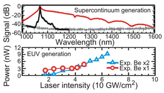
掺鐿光纖雷射與放大器 (ytterbium-doped fiber laser and amplifier) 可在一免校準光路且可靠又堅固的全光纖架構下,結合多模態且連續輸出的半導體幫浦雷射,高效率且穩定地產生熱光效應與光束品質佳的高功率雷射光束。本論文使用具高調制性的單模態半導體奈秒雷射作為波長1064 nm的種子源,並建立一套全光纖主從式掺鐿光纖雷射放大器系統(master-oscillator power amplifier),在數奈秒的時寬下,其輸出能量可達毫焦耳級,整體系統的能量增益與光轉換效率為>63 dB 與>56%。藉由結合雷射放大與非線性波長轉換以避免顯著的驅動能量耗盡,以及預放大器系統的最佳化設計,可成功地在線性偏振輸出的功率放大器中產生峰值功率突破百千瓦的奈秒寬頻連續頻譜 (broadband continuum spectrum),其波長範圍為980 nm到1600 nm且光轉換效率達65%以上。另一方面,在應用端可產生穩定的雷射光聚焦點,強度可達60 GW/cm2,用來形成熱且濃稠的錫電漿源 (hot and dense tin plasma),且初步成功地偵側到極紫外光 (extreme ultraviolet emission) 的訊號。
 |
|
圖一、高強度全光纖奈秒掺鐿光纖雷射主從式放大器系統與其應用端。 |
 |
|
圖二、高功率奈秒超寬頻連續頻譜(上)與錫電漿源激發極紫外光源的初步結果。 |
|
論文題目:氮化鎵元件傳播特性探討
姓名:李季剛 指導教授:吳育任教授
| 摘要 |
|
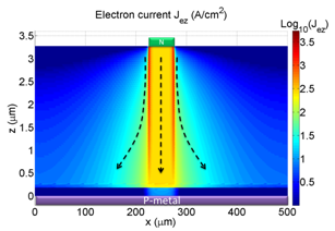
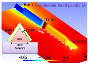
本篇論文利用有限元素法(finite element method)解帕松(Poisson)和漂移-擴散(drift-diffusion)方程式來探討氮化鎵(GaN)元件傳播特性,主要內容為分析氮化銦鎵(InGaN)發光二極體(light-emitting diode)的電流擴佈(current spreading)以及氮化鎵奈米線(nanowire)場效電晶體的短通道效應(short-channel effect)。對傳統水平式發光二極體來說,電流擁擠(current crowding)效應非常的嚴重,我們同時採用模擬結果和電路模型來分析電流擴佈,結果顯示,均勻的透明導電極沒有辦法真的讓電流擴佈非常的均勻。垂直型發光二極體會是一個有效改善電流擴佈的結構,但傳統上的電極設計還沒有最佳化如圖一。所以我們測試不同的電極配置,找出電流擴佈的最佳化來抑制量子井(quantum well)裏平均載子濃度和減少在高電流注入下時的效率衰退。而核殼型(core-shell)奈米線發光二極體比傳統的平面發光二極體有更大的主動區,以及在非極性量子井裡較強的複合,所以藉由增加奈米線的高度得到更大的深縱比,可以增加非極性主動區的體積以減少效率衰退效應(efficiency droop)。另外,圖二為氮化鎵奈米線的示意圖。我們成功模擬50奈米閘極長度氮化鎵奈米線電晶體的實驗結果。而後,我們更進一步討論20奈米的短通道效應。在有更好的環繞閘極(surrounding gate)設計和凹陷閘極(recessed gate)的方法,我們成功抑制20奈米閘極長度的短通道效應。
 |
 |
|
圖一、傳統垂直型發光二極體電子流分佈圖。 |
圖二、奈米線電晶體電位分佈以及結構示意圖。 |
|
|
|
|
|
|
|
|
| |
|
|
|
—
資料提供:影像顯示科技知識平台 (DTKP, Display Technology
Knowledge Platform) —
—
整理:林晃巖教授、張劭宇 —
甲蟲殼般的微透鏡陣列
微透鏡陣列有許多方面的應用,例如可以應用於晶片上光學實驗室(optical lab-on-a-chip devices)、儲存裝置、光伏元件,目前製作這種微透鏡陣列的方法只能應用在平坦的基板上,而且因為製程有許多步驟,因此相當耗時。如今,法國CNRS的Chloé Bayon、Gonzague Agez和Michel Mitov等學者(Lab Chip 14, 2063–2071; 2014),開發了一種只需要一道製作程序就可以製作出膽固醇液晶微透鏡陣列之製程,並且可以將其製作於曲面或可撓曲的基板上;重要的是,此微透鏡陣列的聚焦與光束整形之功能可以隨波長調變。
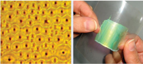
不像傳統透鏡是藉由透鏡形狀來產生聚焦功能,這種最新的微透鏡是依靠膽固醇液晶本身的螺旋結構而產生光束整形的能力,它們是由一群多邊形的膽固醇液晶所組成,每個多邊形扮演著一維光子晶體(布拉格光柵)的角色,並且其週期是由膽固醇液晶之螺距所決定,這種微透鏡陣列就如同天然物種,例如:甲蟲的殼一般。
此陣列是在混入一些膽固醇液晶寡聚物後,經由退火以及快速冷卻而成的;在退火的過程中,多邊形的陣列就會開始成形,如圖1所示,退火之後再快速冷卻形成最終的微透鏡陣列結構。
|
 |
|
圖1、甲蟲殼般的微透鏡陣列 |
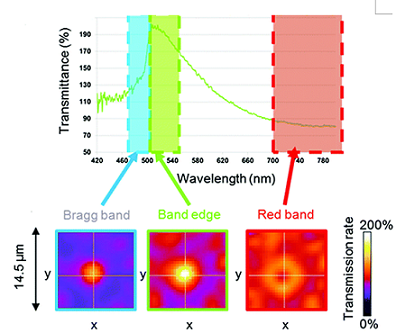
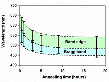
研究人員藉由共軛焦顯微鏡與頻譜儀來分析微透鏡陣列的光學特性,他們將此液晶結構分為三個操作頻譜區域:布拉格區、邊界區以及紅光區,如圖2所示,在布拉格區與邊界區中,焦平面位於此微透鏡陣列之外,此時微透鏡陣列的功能猶如凸透鏡一樣;在紅光區中,焦平面會與陣列平面互相重疊,並且會產生甜甜圈形狀般的光強度分布;布拉格以及邊界區隨著退火時間越長其頻譜特性會藍移,如圖3所示。
|
 |
|
圖2、三種操作頻譜區間以及對應之穿透率示意圖 |
|
 |
|
圖3、布拉格以及邊界區隨著退火時間越長其頻譜特性會產生藍移現象 |
整個團隊的領導人Michel Mitov在Nature Photonics中指出:這種透鏡陣列是一個可以整合在晶片上光學實驗室的多功能微型元件;而且還提供了多種光處理功能、無縫式的整合和機械穩定性等好處。在未來,這個團隊打算在液晶結構中再額外加入一些染料,以研發微型雷射陣列。
|
參考資料: |
1. Simon Pleasants, Micro-optics: Beetle-like microlens array,
Nature Photonics 8, 505, (2014). doi: 10.1038/nphoton.2014.148, Published online: 27 June 2014.
http://www.nature.com/nphoton/journal/v8/n7/full/nphoton.2014.148.html
2. Chloé Bayon, Gonzague Agez, and Michel Mitov,
Wavelength-tunable light shaping with cholesteric liquid crystal microlenses, Lab Chip,
14, 2063-2071, 2014. DOI: 10.1039/C4LC00152D, Published online: 2 May 2014.
http://pubs.rsc.org/en/content/articlehtml/2014/lc/c4lc00152d
|
|
|
|
|
|
|
|
|
|
|
|
|
|
|
|
|
|
 |
|
 |
|