|
|
 |
| |
發行人:林清富所長 編輯委員:陳奕君教授 主編:林筱文 發行日期:2010.12.15 |
| |
|
 |
|
 本所孫啟光教授榮獲中華民國光電學會「九十九年光學工程獎章」,特此恭賀!
本所吳忠幟教授執行有機光電顯示器跨學門科技人才培育計畫,榮獲
「教育部98年度大學跨學門人才培育銜接計畫~優良計畫優等獎」,特此恭賀!
本所12月份演講公告:
|
日期 |
講者簡介 |
講題 |
地點 |
時間 |
|
光電論壇 |
|
12/21 (Tue) |
Prof. Ming C. Wu
Department of
Electrical Engineering and
Computer Sciences & Berkeley
Sensor and Actuator Center,
University of California,
Berkeley |
Semiconductor
Nanolasers |
博理館
101演講廳
|
10:00~12:00 |
|
|
 |
|
 |
|
| |
|
|
|
|
|
|
|
|
11月份「光電論壇」演講花絮(花絮整理:姚力琪) |
|
時間: |
99年11月4日(星期四)上午10點 |
|
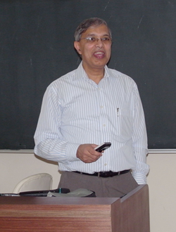
講者: |
古培正教授(Department of
Electrical Engineering and Computer
Science, University of Michigan) |
|
講題: |
Scaling of Semiconductor
Lasers and Solar Cells Using Plasmonics |
|
|
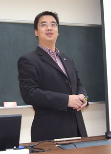
古培正教授於11月4日(星期四)蒞臨本所訪問,並於電機二館105演講廳發表演說,講題為「Scaling
of Semiconductor Lasers and Solar Cells
Using Plasmonics」。 |
| |
|
|
時間: |
99年11月12日(星期五)下午3點30分 |
|
講者: |
陳坤基教授(State Laboratory of
Solid State Microstructures and
Department of Physics, Nanjing
University) |
|
講題: |
Silicon Based Photonic
Quantum Dots and Photonic Molecules |
|
|
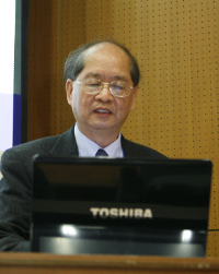
陳坤基教授於11月12日(星期五)蒞臨本所訪問,並於博理館101演講廳發表演說,講題為「Silicon
Based Photonic Quantum Dots and Photonic
Molecules」。陳教授的主要研究領域包括奈米半導體材料、奈米量子電子學和奈米光電子學,本所教師及學生皆熱烈參與演講活動,陳教授演講內容精彩,演講時面面俱到,與本所師生互動佳。 |
| |
本場演講者陳坤基教授
|
|
時間: |
99年11月30日(星期二)上午10點30分 |
|
講者: |
Prof. Ajoy Kar(Physics
Department, Heriot Watt University) |
|
講題: |
Laser Written Active and
Passive Waveguide Devices |
|
|
Prof. Ajoy Kar於11月30日(星期二)蒞臨本所訪問,並於電機二館105演講廳發表演說,講題為「Laser
Written Active and Passive Waveguide
Devices」,本所教師及學生皆熱烈參與演講活動,獲益良多。 |
| |
本場演講者Prof. Ajoy Kar
|
|
時間: |
99年12月1日(星期三)上午10點30分 |
|
講者: |
Prof. Min Qiu(KTH Royal
Institute of Technology) |
|
講題: |
Plasmonic Metamaterial
Absorber at Optical Regime |
|
|
Prof. Min Qiu於12月1日(星期三)蒞臨本所訪問,並於電機二館105演講廳發表演說,講題為「Plasmonic
Metamaterial Absorber at Optical
Regime」。Prof. Min Qiu演講內容豐富精彩,與現場同學互動性佳,本所師生皆獲益良多。 |
| |
本場演講者Prof. Min Qiu
|
|
時間: |
99年12月2日(星期四)上午11點 |
|
講者: |
林清隆教授(Bell Labs and Bellcore (USA, retired);
Formerly Professor of Photonics and
Director, Center for Advanced Research
in Photonics, Chinese University of Hong
Kong) |
|
講題: |
光纖通訊與寬頻全球網路---向2009諾貝爾物理桂冠高錕教授致敬 |
|
|
2010
年是低損耗光纖誕生四十周年紀念。專為高速長程通信系統而開發的光纖,以其幾乎無限的通信容量完全改變世界。現今透過廣泛部署的全球光纖網路啟用,已在世界各地形成寬頻資訊基礎設施,展現功能強大與無遠弗屆的高速電信能力。2009年10月,香港中文大學前校長高錕博士
(Prof. Dr. Charles
K.
Kao),光纖通訊開拓史中的先驅者,以其催生低損耗光纖這個無與倫比的貢獻,與發明CCD
數位電子成像設備的貝爾實驗室波義耳博士(Dr. W.
Boyle)與史密斯博士(Dr. G.
Smith),共同榮獲2009諾貝爾物理學獎桂冠。本講座內容包括在光子學與光纖通信研發的早期故事,以及光纖與全球寬頻互聯網對現代人類資訊社會的重要影響。謹以這個研討會特別演講為頌詞,盛讚高錕教授諾貝爾物理獎榮耀。 |
 |
 |
| 本場演講者林清隆教授 |
2009諾貝爾物理桂冠高錕教授來訪電機資訊學院 |
|
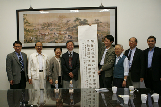
高錕教授夫婦(左三及左四)接受電機資訊學院李琳山院長(右三)致贈紀念品,並於院長室合影留念
|
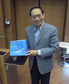
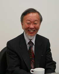
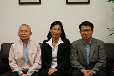
本所特聘講座教授孟懷縈博士來訪—(99年11月16日) |
|
本所特聘講座教授孟懷縈博士,於11月16日回到臺大電機系發表演說,講題為「Engineer,
Educator, and
Entrepreneur」(工程師、教育家和企業家),並分別和教師、學生對談。 |
|
|
|
本所特聘講座教授孟懷縈博士(中),與電機資訊學院李琳山院長(左)、本所林清富所長(右)於院長室合影 |
|
|
|
|
|
|
| |
|
|
|
|
~
與南京大學(Nanjing University)博士生交流活動 2010 系列報導 ~
【2010
兩岸光電科技博士生論壇】
(The 3rd
Cross-Strait Ph.D. Student Forum on Photonic
Science and Technology, 2010)
(時間:99年10月25日至10月26日;地點:臺灣大學)
【之三】
花絮整理:光電所博士班學生蘇亮宇
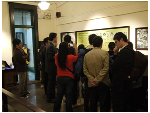
在第三屆南京大學與臺灣大學博士生交流活動中,對岸來的四位老師與十五位博士生進行了為期五天的參訪活動,在這一系列的活動中,前兩天為正式的交流研討會,而在研討會結束之後,我們也規劃了一系列的參訪行程,包括校內的臺大物理文物廳、光電所製程實驗室、故宮博物院、中正紀念堂、台北101等處,以及台灣積體電路、圓展科技等臺灣知名企業。
第三天的參訪活動從臺大物理文物廳開始,展館內主要展示亞洲最早期Cockcroft-Walton型直線加速器及其相關科學文物,由於參訪團的成員主要皆為物理背景,因此對於這些文物表現出高度興趣,特別是帶團的王振林副院長,更不時與導覽員展開熱烈討論。結束了文物廳的行程後,一行人漫步前往電機二館,我們也為參訪團員導覽了椰林大道、總圖等臺大知名地標,在電機二館內我們參訪了光電所製程實驗室、吳志毅老師實驗室、林恭如老師實驗室,在光電所製程實驗室的參訪中,參訪團員對於光電所有如此完善之公用設備感到讚賞,在吳志毅老師與林恭如老師實驗室參訪中,也對於臺大光電在前端研究之潛力感到敬佩。緊接著下午的行程我們前往故宮博物院、中正紀念堂、台北101等處,與他們分享臺灣與中文的文化之美。
除了臺大的校園、光電所實驗室以及一些文化景點之外,我們也規劃了臺灣知名企業的參訪行程,因此我們驅車前往新竹,參觀的第一站為全球積體電路製造的龍頭台積電,導覽的魏烈恒經理極為禮遇我們,一直強調將所有團員當作貴賓看待,並且也詳細地為我們介紹台積電,參訪團員對於台積電驚人的製造能力也感到極為讚嘆,在Q&A時間也不停的展開熱烈的討論,在導覽結束後魏經理也展現地主之誼,邀請我們一同到台積電員工餐廳用餐,體會一些台積電不同的面向。接著我們驅車前往中和圓展科技,圓展科技由張永哲總經理、丁元迪副總經理等重量級人物接待我們,並且全程參與了整個參訪活動,顯示了他們對此活動的高度重視,此外圓展也精心規畫了產品展示的活動,除了派出各研發小組的人解說之外,也以實際操作的方式展示給我們看,因此我們也在充滿收穫之下結束了參訪的活動。
一系列的交流活動就在周末於飯店前的送行之後結束,臺大代表與參訪團員依依不捨地道別,期待明年臺大代表到南京的參訪,也能對雙方的研究迸發出更多的刺激。
【之四】
花絮整理:光電所博士班學生洪士哲
第三屆臺灣大學與南京大學博士生交流活動由臺灣大學規劃舉行,由南京大學物理學院祝世寧院長率領4位老師與15位學生來訪。整個活動的安排包括了論文發表研討會、實驗室參訪、校園巡禮及企業參訪。交流研討會於10月25日及10月26日正式舉行,會議內容相當豐富深入,議程包括nonlinear
photonic devices, solid-state lighting and
display, integrated optics devices, laser
optics and optical devices, nano-photonics,
and optoelectronic
materials等主題,每位代表團學生成員有二十五分鐘的演講時間,演講內容包括本身實驗室簡介與個人研究成果報告,會議期間除吸引多位非雙方代表團成員的學生前來共襄盛舉外,多位光電所的老師亦親臨會場給予與會者寶貴的建議與鼓勵,為此次交流活動增色不少。在兩天精采的學術交流中,我們充分感受到南京大學等大陸學校在研究工作上的投入與傑出成就,每位代表南京大學出席此次交流活動的學生代表都有相當高水準的研究成果,很高興可以和如此優秀的朋友互相學習激盪。
在學術交流之外,我們也安排了文化參訪及企業參訪的行程,讓遠道而來的老師及學生可以體會臺灣在地的風俗民情及文化。我們安排參觀了國立故宮博物院、中正紀念堂、台北101等著名景點,同時也到了野柳、九份及士林夜市等地區性觀光地點。在與南京大學的學生們聊天時得知,其實他們多數同學是第一次出國,而且由於經費問題,他們幾乎很少有機會到歐美國家開會參訪,絕大部分參加的會議都是在國內,所以他們也非常珍惜這次的交流活動。這也讓我感受到應該更加珍惜我們所擁有的資源及機會。離開臺灣時,他們帶走了十多箱的鳳梨酥、茶葉及其他臺灣名產,也算是為臺灣經濟做出了些許的貢獻。
此外,我們安排南京大學代表團參訪相關實驗室、研究中心及公司。除了參觀所上多位老師的實驗室外,還參觀了物理系舊館。南京大學物理系代表團的老師學生都對臺大物理系的歷史非常有興趣。同時,我們亦安排參觀臺灣優秀的企業,包含到新竹參觀台積電與台北的圓展科技的行程,感謝所有提供參觀協助的單位,讓南京大學物理系代表團可以有如此豐富的參訪行程。
藉由參與此次活動,除了認識來自南京大學的朋友之外,也很高興可以與其他同為光電所代表團學生成員的博士生更為熟悉,謝謝大家為整個交流活動的付出,大家辛苦了。最後,感謝光電所為我們開啟了和南京大學物理學院進行交流的機會,也感謝老師林清富所長的推薦,使我得以在從事本身的研究工作之外,代表光電所和南京大學物理學院優秀的研究生進行學術交流。這是相當珍貴的經驗與學習機會。最後,也感謝所辦林筱文小姐為此活動所付出的心力,才能讓活動如此成功。希望如此有意義的交流活動可以一直持續下去,讓更多光電所的學生可以親自體驗與學習。
 |
 |
|
大陸老師及學生們參觀物理舊館 |
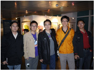
臺灣學生及大陸學生於台北101合照 |
|
|
|
|
|
|
|
|
| |
|
|
|
|
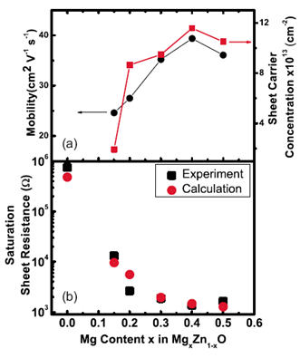
Two Dimensional Electron Gases in Polycrystalline MgZnO/ZnO
Heterostructures Grown by RF-Sputtering
Process
Professor I-Chun Cheng's group
Graduate Institute of Photonics and
Optoelectronics, National Taiwan
University
臺灣大學光電所 陳奕君教授
We study the formation of
two-dimensional electron gas (2DEG) in
rf-sputtered defective polycrystalline
MgZnO/ZnO heterostructure via the
screening of grain boundary potential by
polarization-induced charges. The sheet
resistance reduces rapidly and then
saturates as the MgZnO thickness
increases. Both the mobility and the
sheet carrier concentration in
saturation increase as the Mg content is
raised and reach maxima of 39.4 cm2V-1s-1
and 1.15x1014cm-2
at x=0.4, confirmed by low temperature
Hall measurement. Monte Carlo method by
including grain boundary scattering
effect as well as 2D
finite-element-method Poisson and
drift-diffusion solver is applied to
analyze the polycrystalline
heterostructure. The experimental and
simulated saturation sheet resistance
show good agreement. Both carrier
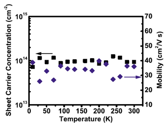
concentration and mobility are
temperature independent, indicating the
formation of 2DEG with roughness
scattering at the MgZnO/ZnO interface.
Our result suggests that polycrystalline
MgZnO/ZnO material system can be a
potential candidate for the application
of low-cost large-area high electron
mobility transistor (HEMT) devices.
|
 |
|
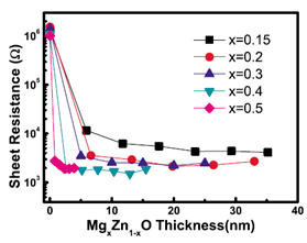
Figure 1. Sheet resistance of
polycrystalline MgxZn1-xO/ZnO
heterostructure versus thickness of MgxZn1-xO
cap layer for x=0.15, 0.2, 0.3, 0.4, and
0.5. The lines are guides to the eyes. |
|
 |
|
Figure 2. (a) Hall
mobility and sheet carrier concentration
of MgxZn1-xO/ZnO
heterostructure in saturation as
functions of Mg content x. (b)
Comparison of experimental and
calculated saturation sheet resistances
as functions of Mg content x. The lines
are guides to the eye. |
|
 |
|
Figure 3. Hall mobility
and carrier concentration of Mg0.3Zn0.7O/ZnO
heterostructure with Mg0.3Zn0.7O
capping layer thickness of ~30 nm as
functions of temperature. |
Study of Carrier Dynamics and Radiative Efficiency in InGaN/GaN LEDs
with Monte Carlo Method
Professor Yuh-Renn Wu
Graduate Institute of Photonics and
Optoelectronics, National Taiwan
University
臺灣大學光電所 吳育任教授
In a LED, carriers are
injected from the contacts and diffuse
laterally in the quantum wells (QWs). In
this paper, we apply the Monte Carlo
(MC) method to study the carrier
dynamics in the InGaN QW. The radiative
recombination rate is calculated by a
self-consistent Poisson,
drift-diffusion, and Schrodinger solver.
We set different dislocation densities
and trap cross sections of threading
dislocation, and study the influences to
the device efficiency by MC method. The
effects of alloy scattering, charged
dislocation scattering, interface
roughness scattering, and e-e scattering
are included in our MC model. The
locations of dislocations are arranged
randomly and are depending on
dislocation densities. The electron will
diffuse randomly by scattering in the QW
before recombination. If the electron
incidents into the location of the
threading dislocation, it is captured by
the threading dislocation and recombines
non-radiatively. The diffusion ranges
and the captured chances are influenced
by many scattering mechanisms and will
be discussed in this paper.
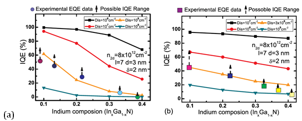
Our simulation result shows a strong
dependence on the indium composition
because of the longer radiative lifetime
in the longer wavelength due to QCSE.
The carrier diffusion length with higher
In composition increases because of a
longer radiative lifetime. However, the
diffusion length in a higher In
composition QW will decrease if the
interface roughness scattering is very
strong. The larger diffusion length
leads to a higher capture rate. To
estimate the internal quantum efficiency
(IQE), we need to define the carrier
capturing cross section diameter, δ. The
published TEM results show the threading
dislocation has a carrier trapping
diameter around a few nanometer. Within
these ranges, we start to estimate the
expected IQE. We find that with a larger
interface roughness, the IQE can be
improved by a few percent. If the δ
changes from 2nm to 4nm, the radiative
efficiency will decrease 20% to 30%. If
the dislocation density drops to 106
cm-2, the IQE can be improved
significantly. Since most LEDs are the
lateral LED, there would be a lateral
electric field in QW with a larger
applied bias. Our results show the
efficiency will drop 30% to 70%
depending on the In composition when
applying a small lateral electric field.
The carrier is easier to be captured if
it is drifting with a certain direction
rather than diffusing in a random
direction. This indicates that non-radiative
coefficient, A, is not a constant and
should be strongly dependent on the
bias, δ, and dislocation density. Our
estimated IQE is compared with published
experimental results and shows a good
agreement in the trend. Our results show
that for the longer wavelength source,
we should try to decrease the radiative
lifetime by reducing the QCSE with a
nonpolar/semipolar structure. The other
way is to reduce the dislocation density
to be lower than 106 cm-2.
However, both should be achieved to make
the IQE reaching 100%.
|
 |
|
Fig. 1 (a) Estimated maximum
efficiency versus indium
composition for different
dislocation density values when
n2d is 8x10¹²
cm-2. Also shown is a
comparison with experimental
results. (b) Estimated e±ciency
versus indium composition with
different dislocation densities
for the nonpolar plane cases. |
|
|
|
|
|
|
|
|
| |
|
|
|
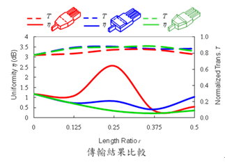
論文題目:多模干涉分光器之改良設計
姓名:魏佐芸 指導教授:王維新教授
| 摘要 |
|
本文探討截角式、加高式、結合式等三種特殊多模干涉一對多分光器(Multimode interference power splitters)。所謂截角式是考慮多模波導寬度有變化,加高式是考慮多模波導高度有變化,而結合式則是同時考慮截角與加高兩種變化。模擬結果顯示前兩種變化加在多模波導的入射區時都可以提升多模干涉分光器的傳輸率(normalized transmission power)及減小不均勻度(uniformity),而且元件的干涉長度也可以縮短;第三種結合式則有兩者加成之效果。
|
 |
 |
|
圖一:漸變加高式多模干涉分光器 |
圖二 |
|
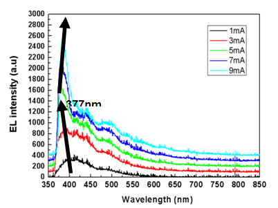
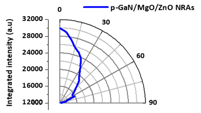
論文題目:高效能可見光及紫外光發光二極體及其奈米結構之研究
姓名:柯閔詠 指導教授:黃建璋教授
| 摘要 |
|
我們利用射頻濺鍍(RF-sputtering)成長具有載子侷限結構之氧化鋅(ZnO)異質pn接面發光二極體,具有二氧化矽電流阻擋層(SiO2 current blocking layer)之元件,其發光頻譜峰值為394nm並大幅降低缺陷發光。而具有載子三明治侷限結構之元件,能使載子能夠更有效注入及侷限於氧化鋅發光層,達到377nm近紫外波長放光。
我們亦製作一具高光指向性之紫外光氧化鋅奈米柱(ZnO nanorods)/氮化鎵 (GaN)發光二極體。並在其界面加入一氧化鎂電子阻擋層,透過此結構之設計,達到390nm近紫外放光,此元件顯示出高度之光指向性且其發散角為30度,顯示具奈米柱結構之氧化鋅發光元件具有成為高指向性UV發光源之潛力。
|
 |
|
Fig. 1 EL spectra of the GZO/ZnO/GaN
LED with SiO2
barriers. |
|
|
 |
|
Fig. 2 Radiation patterns of p-GaN/MgO/ZnO
naoarod arrays exhibits
waveguiding effect. |
|
|
|
|
|
|
|
|
|
| |
|
|
|
—
資料提供:影像顯示科技知識平台 (DTKP, Display Technology
Knowledge Platform) —
—
整理:林晃巖教授、陳韋仲 —
「用水就能製作半導體」,美國倫斯勒理工學院成功在石墨烯中形成能帶隙
美國紐約倫斯勒理工學院(Rensselaer Polytechnic
Institute)宣佈,該校研究人員成功地使用水在石墨烯中形成能帶隙。論文已刊登在學術雜誌《small》上。
石墨烯本身並沒有能帶隙,只具有與金屬一樣的導電特性。在此研究中證明了使用簡單的方法即可使石墨烯產生能帶隙。倫斯勒理工學院教授Nikhil
Koratkar表示,此研究嘗試的關鍵是「破壞石墨烯的對稱性」。石墨烯沒有能帶隙主要是由於石墨烯薄膜具有高度對稱性,只要能破壞該對稱性,就能在其中形成能帶隙。Koratkar教授的研究團隊首先在二氧化矽底板上製作出石墨烯薄膜,然後將薄膜和底板一起放入保持一定濕度的容器中。藉此石墨烯吸收空氣中的水分後,進而形成能帶隙,此研究使用的方法是控制濕度使石墨烯薄膜表面吸收水分子,而與二氧化矽底板相接的那一面則無吸收,從而破壞了薄膜的對稱性。而且可透過調節濕度,在0~0.2
eV的範圍內可精確地設定能帶隙值。這種變化是可逆的,只要放入真空中,就可使已形成的能帶隙值回歸於0。
在透過破壞對稱性形成能帶隙的方法上,將石墨烯加工成細帶狀、以及利用兩層或三層石墨烯等方法也都被開發出來。Koratkar表示,「此次的方法具有低成本、無毒性以及帶隙調節非常簡單」的優點。此研究有助於使用石墨烯製作電晶體、二極體、奈米電子及奈米光子等應用。
|
 |
|
圖一、
在二氧化矽底板上製作出的石墨烯薄膜、分析其導電性 |
|
中文新聞來源: |
http://big5.nikkeibp.com.cn/news/semi/53807-20101028.html |
|
英文新聞來源: |
http://news.rpi.edu/update.do?artcenterkey=2783&setappvar=page%281%29 |
|
論文來源: |
“Tunable Band
gap in Graphene by the Controlled Adsorbtion of
Water Molecules,”
published by the journal Small.
http://dx.doi.org/10.1002/smll.201001384
|
|
|
|
|
|
|
|
|
|
|
|
|
 |
|
 |
|