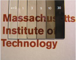
|
The
Correlation of Turn on Voltage and Band
Alignment in Organic Light Emitting Diodes
Professor Chih-I Wu
Graduate
Institute of Photonics and
Optoelectronics, National Taiwan
University
臺灣大學光電所
吳志毅教授
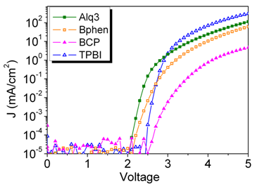
Turn on
voltage in the current density-voltage
characteristics is one of the important
factors to evaluate the performance of
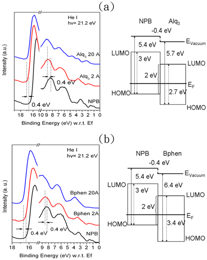
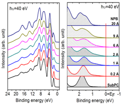
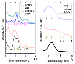
organic light emitting diodes (OLEDs). We report investigation
of the origins of turn-on voltage,
defined at where log J (current density)
has a sharp rise and starts to increase
dramatically. In OLEDs with NPB as the
hole transport layer (HTL) and Alq3
as the electron transport layer (ETL),
we find that the turn on voltage is
always at 2V, regardless the cathode
structures being used, such as Ca, Al,
LiF/Al and Cs2CO3/Al.
The turn on voltage is also independent
on the thickness of organic layers
(thickness varies from 30nm to 120 nm).
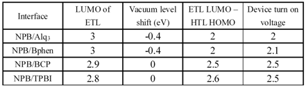
Beside NPB and Alq3,
we also study the J-V characteristics on
various OLEDs with T3/Alq3,
NPB/T3,
and NPB/Bphen as HTL/ETL, respectively.
In all the devices mentioned above, the
turn on voltage just equals to the
difference between the LUMO of ETL and
the HOMO of HTL, taking into
consideration of vacuum level shift at
organic interfaces measured from the
ultraviolet photoemission spectroscopy
(UPS). Combined with J-V characteristics
of OLEDs and UPS measurement, we
conclude that the turn on voltage of
organic light emitting devices is
determined by the difference between
LUMO of ETL and HOMO of HTL and is
independent of the cathode and thickness
of organic layers. We also found that
the charge transfers at the interface of
ETL/HTL play an important role to the
turn on voltage of OLEDs.
Emitting
Layer Thickness Dependence of Color
Stability in Phosphorescent Organic
Light-Emitting Devices
Professor
Jiun-Haw Lee
Graduate Institute of Photonics and
Optoelectronics, National Taiwan
University
臺灣大學光電所 李君浩教授
We
investigated the strong influence of the
thickness of iridium(III)bis[(4,6-difluorophenyl)
-pyridinato-N,C2’]picolinate
(FIrpic) doped N,N’-dicarbazolyl-3,
5-benzene (mCP) blue emitting layer (B-EML)
on color stability. The large voltage
drop across the B-EML resulted in a
higher sensitivity of the carrier
transport and injection properties to
the applied external voltage. According
to carrier mobility measurements by the
time-of-flight method, the electron
mobility of the mCP exhibited a strong
dependence on the electric field.
Therefore, at a higher driving voltage,
the more rapidly increasing electron
mobility of the mCP and the decreasing
energy barrier height on the electron
transport path would extend the
recombination zone from the B-EML to the
tris(phenylpyridine)iridium (Ir(ppy)3)
doped mCP green emitting layer (G-EML)
in devices with thinner B-EMLs. Coupled
with the fluctuations of the
recombination zone, stronger
triplet-triplet exciton annihilation
occurring in the thinner B-EMLs led to
an even more evident deterioration of
the color stability. After circumventing
these two negative factors, a green-blue
organic light-emitting device (OLED)
with ultra-high color stability was
demonstrated, with the CIE coordinates
slightly shifted from (0.256, 0.465) to
(0.259, 0.467) with increased luminance
from 48.7 to 12700 cd/m2.
Further adding a red phosphorescent
dopant into this green-blue EML
backbone, we successfully fabricated a
white OLED with high color stability,
which exhibited a nearly invariant CIE
coordinate throughout the practical
luminance range from 1050 ((0.310,
0.441)) to 9120 cd/m2
((0.318, 0.446)) and maximum
efficiencies of 26.4 cd/A and 19.8 lm/W
[published in Org. Electron. 11,
1500, 2010].
Effects
of Gate Bias and Thermal Stress on ZnO
Thin Film Transistors
Professor
Jian-Jang Huang
Graduate Institute of Photonics and
Optoelectronics, National Taiwan
University
臺灣大學光電所 黃建璋教授
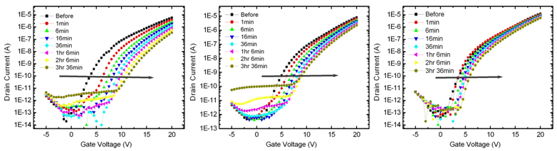
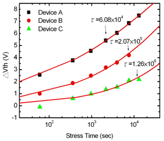
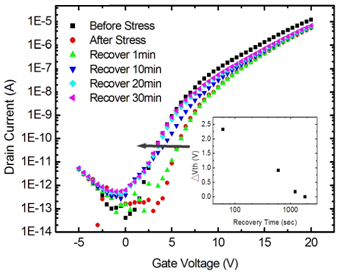
The
effects of gate bias and thermal stress
on the threshold voltage shift were
examined for ZnO TFTs fabricated on the
glass substrate. We compared three
samples with various post ZnO growth
annealing durations. The results show
that the threshold voltage shift (ΔVth)
is only 2.2V after a 1.3×10⁴s
stress at the gate bias 20V for device
C. And the threshold voltage shift can
be correlated to the stress time
following the charge trapping mechanism.
The characteristic trapping time
τ of
device C was calculated to be 1.26×10⁶
s. Further comparisons of the trap
states and off currents reveal that
device C has a better ZnO crystalinity
and a better ZnO/SiNx
interface quality. Finally, the
characteristic trapping time was
extracted at different temperatures for
device C. We obtain an average effective
energy barrier Eτ of 0.57eV.
The results presented in this work
suggested that excellent
τ and Eτ
can be obtained from ZnO TFTs on the
glass substrate following our
fabrication steps.
|
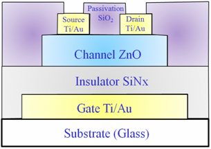 |
Fig. 1: Layer
structure of the ZnO TFT on the
glass substrate.
Fig. 2:
Transfer curves at different stress
time for device A(a), B(b) and C(c).
The bias gate voltage is 20V.
Fig. 3: Time
dependent ΔVth of device A, B and C
under a gate bias 20V.
Fig. 4: Time
evolution of transfer curve during
the recovery phase of device C. The
inset shows the ΔVth versus
relaxation time. |
|
Fig. 2(a) |
Fig. 2(b) |
Fig. 2(c) |
|