|
Analysis of the Optical
Phase Conjugation Phenomenon via PSTD
virtual optical experiments
Professor Snow H.
Tseng
Graduate Institute of Photonics and
Optoelectronics, National Taiwan
University
台湾大学光电所 曾雪峰教授
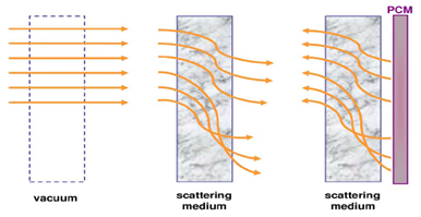
Experimental research of the optical
phase conjugation (OPC) phenomenon
exhibits interesting phenomena that are
yet to be understood. The OPC refocused
light cross-sectional width is observed
to be approximately the same regardless
of the thickness of the scattering
medium. We employ the pseudospectral
time-domain (PSTD) technique to
accurately simulate the OPC refocusing
phenomenon of light propagating through
a macroscopic scattering medium.
Simulation results show that the optical
thickness of the scattering medium is
not directly related to the OPC
refocused light width.
|
 |
|
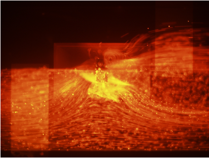
Fig. 1. After
OPC, multiply scattered light propagates
in reversed directions—similar to a time
reversal process. |
|
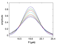
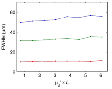
Fig. 2.
(left): Amplitude of the OPC
refocused light pulse for various
thicknesses of the scattering
medium. Top to bottom: 40, 80, 120,
160, 200, 240, 280, and 320
μm,
respectively. (right):
Cross-sectional width of the OPC
refocused light of three different
incident cross-sectional widths
plotted vs. transport mean free path
(μs′×L). |
Light Emission
Polarization Properties of Strained (11-22) Semipolar InGaN Quantum Well
Professor Yuh-Renn Wu
Graduate Institute of Photonics and
Optoelectronics, National Taiwan
University
台湾大学光电所 吴育任教授
We
studied the optical characteristics of a
(11-22) semipolar InGaN/GaN quantum well
with different indium compositions,
quantum well widths, and injection
carrier densities. The self-consistent
Poisson and 6×6 k·p Schrödinger solver
including the effects of quantum
confinement and polarization charges has
been applied to study the band
structures in semipolar InGaN quantum
well light emitting diodes. The
influence of the indium composition,
well width, and injection carrier
density to the (11-22) semipolar quantum
well are studied in this work. The
optical polarization properties are
strongly influenced by the hole
effective mass and the strain effects
especially the shear strain induced in
the semipolar plane. Our studies show
the interesting polarization switching
behavior when the indium composition is
larger than 40%. For the surface
emitting LED, the polarization ratio of
ρyx
′
can be larger than 0.4
when the indium composition is smaller
than 40%. This shows a great opportunity
of using semipolar InGaN quantum well
LED instead of c-plane case.
 |
 |
|
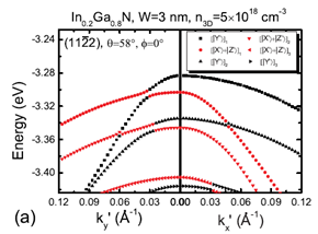
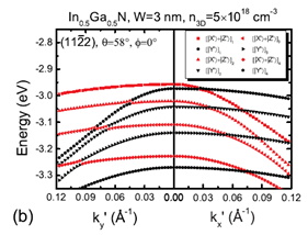
Figure 1 (a)
and (b) are the calculated valence band
dispersion relations of the (11-22)
semipolar InxGa1−xN/GaN quantum well for
x=0.2 and x=0.5, respectively. |
|
 |
|
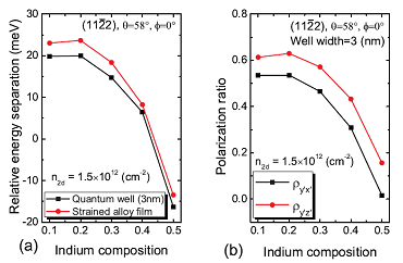
Figure 2 (a)
The relative energy separation of (11-
22) InGaN/GaN quantum well structure and
the strained InGaN alloy film as a
function of indium composition. (b) The
polarization ratios of the InGaN/GaN
(11-22) quantum well as a function of
indium composition. |
ZnO/Al2O3
core–shell nanorod arrays: growth,
structural characterization, and
luminescent properties
Professor J. H. He
Graduate Institute of Photonics and
Optoelectronics, National Taiwan
University
台湾大学光电所 何志浩教授
We
demonstrated an aqueous chemical method
to fabricate well-aligned ZnO/Al2O3
nanocrystal (NC) core–shell nanorod
arrays (NRAs). Structural
characterization showed that the shell
layers are composed of α-Al2O3
nanocrystals. Photoluminescence
measurements showed the enhancement of
near-band-edge (NBE) emission of ZnO
NRAs due to the presence of Al2O3
NC shells. The Al2O3
NC shell layer resulting in the
flat-band effect near the ZnO surface
leads to a stronger overlap of the
wavefunctions of electrons and holes in
the ZnO core, further enhancing the NBE
emission. This approach should be very
useful in designing many other
core-shell NRAs for creating varieties
of high-efficiency optoelectronic
devices.
|
 |
|
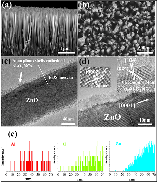
Figure 1. (a) A
cross-sectional SEM image, (b) a
top-view SEM image, (c) a TEM image, and
(d) an HRTEM image of ZnO/Al2O3
core–shell NRAs (sample C). The left and
right insets in (d) are the HRTEM images
of the ZnO core and Al2O3 shell,
respectively. (e) The linescan of EDS
analysis for ZnO/Al2O3
core–shell NRs in (c). |
|
 |
|
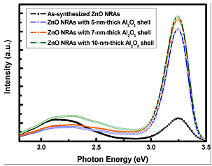
Figure 2. PL
spectra of the ZnO and ZnO/Al2O3
NC core–shell NRAs at room temperature. |
|