 |
||||||||
|
|
||||||||
|
�����ˣ����������� �༭ίԱ������ܽ��� ���ࣺ������ �������ڣ�2008.09.03 |
||||||||
|
�� |
||||||||
|
��
ʱ�䣺2008��8��11������10��30��~11��45��
���ߣ�Prof.
Ray T. Chen (Nanophotonics and Optical Interconnects Lab., Department of
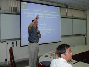
Electrical and Computer Engineering, The University of Texas, Austin) Prof. Ray T. Chen��2008��8��11��(����һ)ݰ�ٱ������ʣ����ڵ������142�����ҷ�����˵������Ϊ��Silicon- and Polymer-based Nanophotonic Devices for Optical Communications����������ʦ��ѧ�������Ҳ����ݽ��������������
ʱ�䣺2008��8��25������3��
���ߣ���������ڣ�Joint
Research Center of Photonics of the Royal Institute of Technology
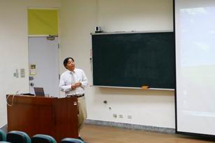
(Sweden) and Zhejiang University (China)�� �����������2008��8��25��(����һ)ݰ�ٱ������ʣ����ڵ������105�ݽ���������˵������Ϊ��Improving the performances and functionalities of photonics devices with subwavelength-structures and nanoparticles����������ʦ��ѧ�����Ҳ����ݽ����
�� |
||||||||
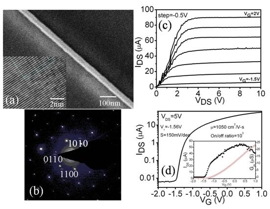
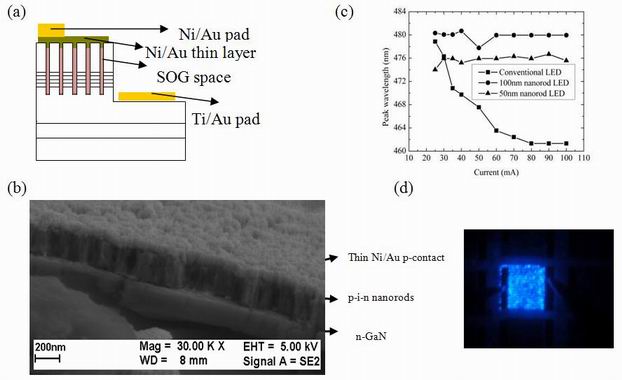
�� Ferroelectric nitride-oxide nanowire MOSFET and phase change memory Professor Lung-Han Peng's group Graduate Institute of Photonics and Optoelectronics, National Taiwan University (e-mail) peng@cc.ee.ntu.edu.tw ̨���ѧ�������¡嫽��� A. Nitride-oxide nanowire MOSFET
We demonstrated a selective growth of high crystallinity
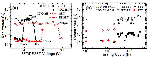
�� B. Nitride-oxide phase change memory We report a new type of phase-change materials based upon the compound of In-Ga-O. It is found to exhibit two-order of magnitude resistivity change between the high-resistive amorphous phase and the low-resistive cubic phase at a phase-change temperature ~250��C. When the In-Ga-O is incorporated into a nonvolatile phase change memory (PCM) device with a double-heater (DH) structure, it exhibits an on/off resistance ratio of 1000 and cycling over 300 times which are superior to those observed on a single-heater (SH) PCM device. These results, together with a low bias point of 70mA at 6.5 volt and 1.5mA at 3.5 volt, respectively, for set/ reset operation of the DH-PCM device to the crystalline/amorphous state, suggest that In-Ga-O is a promising material candidate for low power application of PCM devices. ��
|
||||||||
|
�� ������Ŀ�������ڹ�ѧ����Ƶ����Ӱ������ �����������M ָ�����ڣ����������
�� �� |
||||||||
|
�� �� �����ṩ��Ӱ����ʾ���Ƽ���ɫ�˲��������ģ�Ӱ����ʾ�Ƽ�֪ʶƽ̨ �� �� �������ֻ��ҽ��ڡ��¹��� �� ��
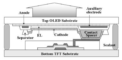
���Ϻ�LG��ʾ�����OLED��忪�����˳�Ϊ��DOD����Dual-plate OLED Display�����������ṹ������SID 2008��ͷ����3.2�з�����������һ�ṹ��15���л�EL�������Ʒ��Ҳ��SID 2008չʾ�᳡��չ������ͼһ���� ��
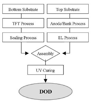
�� ������DOD�ṹ���л�EL��������鲣���װ幹�ɡ���һ�鲣���װ����γɱ�Ĥ�����(TFT)����һ�鲣���װ����γ��л�EL�������������TFT������������л�EL���������������ڲ��Ӵ��Ľṹ����ͼ�������ýṹʱ������������ͼ����ʾ���Ϻ�LG��ʾ����Ϊ�������ܹ��ֱ��ؼ����ʾ����������ԭ����һ�鲣���װ����γ�TFT������л�EL������л�EL�����ȣ��ܹ���ֹ��Ʒ�����½��� ��
�� ��15���л�EL���Ļ���Ϊ1024��768���ء����ش�СΪ96��m��297��m���ֱ���Ϊ85.5ppi�����ؿ�����Ϊ52�������ô��л�EL����ĵװ�һ���ȡ��Ķ�������ṹ�� ��
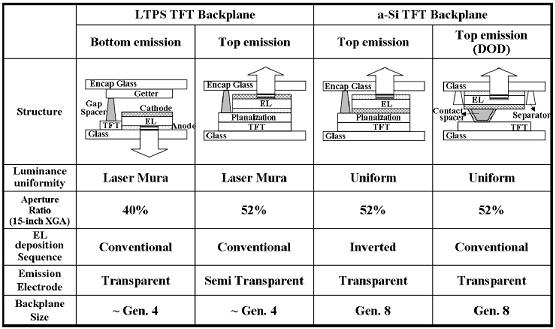
�� ����һ�����ܽ�����������ŵ㡣���¶ྦྷ�象Ĥ�����(LTPS TFT)���·�����ʽ����Ϊ�·��⣬���Կ�����̫С����Ϊ���¶ྦྷ�象Ĥ����ܹ�ϵ�����������Ȳ�����ֻ���õ����Ĵ����塣���¶ྦྷ�象Ĥ����ܵ��Ϸ�����ʽ���������缫Ϊ����������������ģ��������Ч�ʡ��Ǿ��象Ĥ�����(a-Si TFT)���Ϸ�����ʽ���ɴ����ڰ˴����壬��һ·�����������ʲ��ߡ��Ǿ��象Ĥ����ܵ�DOD��ʽ�������������OLED�����TFT�ֿ�������������������ʡ� ��
�� �� �������ų����� http://big5.nikkeibp.co.jp/china/news/news/flat200805230125.html �� �� �� |
||||||||
|
�� �� ������ƿ�������ϳ�ˬ��Ȼ�ó��� �� �д�һ˵ ����������������е��ɻ������������ ����Ҫ�����ţ� �ܶ���ϰ�߳Ա��������һƿ������������һЩ��װ�����ϣ��ųƿ��ԡ�ȥ�ͽ��塹������ȥ�Ǻ�ˬû�д���������û�������������Ķ�����ᷢ��ʲô�£��� �춯����������ɣ���������ţ��(�������ּ���±ζ��)�����������ʳ���θҪ���������ͱȽϳ����ˡ������ٵ���һƿ��ˮ����û�п����������������ţ�Ͱ�������������������Dz�װ��������̽��������𣿶���ij�θ����һ��������������ͣ���ȥʲô�͡���ʲô���֣����ֻ�Ƕ��ĵĻ������ˣ��ص��ǡ���ó���������Щ����������θ����ٶ��ܽ�ɰ�Һ״��Ȼ���ȹ�̬ʳ����һ����������������dz����𤡢�Ͳ���ˮ��ˮ�����ʾͻ����ȱ��������ա����ǣ�������û�а취��ȫ�����ų���Щ��������ʣ������ë��մ����֬���ͺ�����Ҫϴţ�����Ĺ���һ������ôϴ�����Ǿ��������塣���Ҿö���֮���ֶ��ĵĶ����ͻḽ���ڳ������ϡ����ܲ����������ﵹɫ���Ѱɣ��������������µĶѻ����ʱ䣬��Щ����������Ϣ�⣬���п��ܵ��Dz���ɳ����� ���ԸϿ�ĵ�����Ҫ���Ļ�ϰ�ߣ�����Ҫ���Ϲ�����������Ǻȵ��������¿�ˮ�ͺ�����Ȼ��ƽ��û�¶�����̡����̿����ó�������þ���������������ij���������ɨ�����ó������ɾ��� ��
KingNet
Ӫ��������ѯӪ��ʦ�ش��� ������������(����)�����ݣ�������Ϊ�䡸���ߡ��������࣬��̫���ڡ�Σ���������� ������������������ȷ�а����彡�������������Ǻ��µĶ����������ƽ��Ϊ37.5�棬���Թ��ȵ�ʳ�ñ������Ʒ���ͺ���������������ܼ��ˡ����磺��θ���������ط��ڼ��٣�������ɳ�θ�������չ��ܱ�����Է������ؼ��ᣬ�ֿ���Ҳ���ű�������Ҳ����Ϊʲô����������ϱ���ڸ����ԭ��
���ڣ��������Ὣ���͡�ţ�ͱ�ɹ����������������˵�������̫�����ˣ���˵������Ӱ�����£���ȴֻ����ʱ�Եģ��Ͼ������Ǻ��¶�������������������켰���������������������²ʹ�����������ܾ���ָ������Ĺ��ܣ�������θ����Ľ��ػ��ܡ�֬����أ�֬���ֽ���أ���������Ҫ�ֽ�֬���Ľ��أ��������İ�æ�����Ĥ��֯����˳������������������֮��֬���ڱ���������ǰ�����Ѿ���֬����ء����������ˣ���������������˵�ģ���������û�а취��ȫ�����ų���Щ��������ʣ������ë��մ����֬���ͺ�����Ҫϴţ�����Ĺ���һ������ôϴ�����Ǿ��������塣������ʵ����̫С�����������Ĺ��죬��Ҳ��̫���ڡ���ĥ������������١�һ�������ڱ��㷴���ء���ĥ���������ҵ��ڡ�֮�£������磺ϲ������ʳ�サ��ʳ�ã�һ������ͻȻ�������ɣ���ô���п����ò����л��ɳˣ����������κμ����������ʲ��ò�С�Ľ������õ���ʳϰ�ߣ�������ѵ�����֮���� �����ɡ�KingNet ��������ҽԺ���ṩ �� |
||||||||
|
��Ȩ���� ����̨���ѧ�����ϢѧԺ��繤��ѧ�о��� http://gipo.ntu.edu.tw/ ��ӭת�� ����ע������ http://gipo.ntu.edu.tw/monthly.htm |
||||||||