 |
|||||||||||||||||||||||
| |
|||||||||||||||||||||||
|
发行人:黄升龙所长 编辑委员:蔡睿哲教授 主编:林筱文 发行日期:2008.08.01 |
|||||||||||||||||||||||
|
|
|||||||||||||||||||||||
|
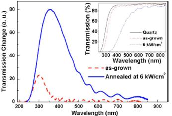
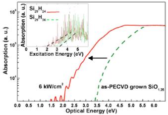
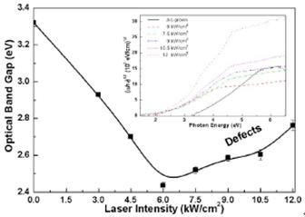
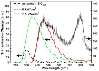
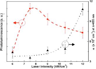
Optical Characterization of CO2-Laser-ablated Si rich SiOx Professor Gong-Ru Lin Graduate Institute of Photonics and Optoelectronics, National Taiwan University 台湾大学光电所林恭如教授 Anomalous absorption and the corresponding change in the optical band gap of a CO2-laser-ablated Si-rich (SiOx) film are studied. The optical band gap energy of as-grown nonstoichiometric SiOx is slightly reduced by increasing Si–Si bonds as compared to quartz. After rapid thermal annealing using a CO2 laser, the dehydrogenation of SiOx film further increases the Si–Si bonding states and redshifts the optical band gap by 1 eV (see Figure 1a and 1b). Laser ablation is initiated at a laser intensity of >7.5 kW/cm2 (see Figure 2), leaving numerous luminescent centers that are related to neutral oxygen vacancy defects, increasing the absorption coefficient and related optical band gap energy, and reducing the refractive index in partially annealed SiOx (see Figure 3a and 3b).
In summary, the anomalous absorption spectra and corresponding changes in optical band gap energy, band edge absorption, and structurally damaged related luminescent centers of the CO2-laser-ablated PECVD-grown SiO1.25 film were characterized using UV-VIS-NIR transmission/ reflection and PL spectroscopies. After PECVD deposition, a slight redshift in the transmission and the lower optical band gap energy of as-grown SiO1.25 in comparison with those of quartz substrate are due to the increase in the Si–Si bonding state in SiO1.25 near the valence and conduction band edges. Since the as-grown SiO1.25 film contains a high concentration of hydrogen, dehydrogenation not only reduces the thickness of the PECVD-grown SiO1.25 film but also enhances the number of Si–Si bonding states under CO2 laser RTA below the ablation threshold (6 kW/cm2), hence contributing to a redshift of the optical band gap from 3.32 to 2.43 eV. As the CO2 laser RTA intensity increases to >6 kW/cm2, the optical band gap energy of the PECVD-grown SiO1.25 increases oppositely from 2.43 to 2.76 eV due to the ablation-induced damage to the surface and the generated NOV defects. The absorption coefficient of the SiO1.25 film at a wavelength of 455 nm is increased by a factor of 3 as the CO2 laser intensity is increased from 7.5 to 12 kW/cm2. During ablation, the incompletely annealed SiO1.25 with numerous oxygendependent defects also suffers from a slight decrease in the refractive indices from 1.87 to 1.79 when Plaser increases from 7.5 to 12 kW/cm2.
|
|||||||||||||||||||||||
|
论文题目:使用新颖材料与组件结构之高效率磷光有机发光组件 姓名:蔡明翰 指导教授:吴忠帜
|
|||||||||||||||||||||||
|
— 数据提供:影像显示光电科技特色人才培育中心.影像显示科技知识平台 — — 整理:林晃岩教授、陈冠宇 —
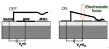
南韩科学与技术学院(KAIST)在SID 2008国际研讨会中,进行编号3-4论文之口头报告,主旨是使用MEMS开关代替驱动有机EL的TFT。此举之用意是在打破以往使用的硅TFT在大屏幕制作时与可靠性方面存在的限制。目前对有机EL的驱动通常是使用硅薄膜晶体管(TFT)。然而目前作为主流的低温多晶硅TFT,对于再结晶制程中所使用的激光退火装置,在大画面组件制程方面仍然存在问题。此外,非晶硅和微晶硅的TFT,则存在着其阈值电压会随时间而变化的问题。
为了解决上述这些问题,KAIST在此次研讨会中提出了使用MEMS开关技术来驱动有机EL。MEMS在显示的应用方面,目前多以其作为光的切换开关,例如:德州仪器的DLP、Qualcomm的iMoD、Silicon Light Machine的GLV;而KAIST所提出的MEMS开关,则是采用脉冲宽度调变(PWM,pulse width modulation)的数字电路来驱动有机EL工作。
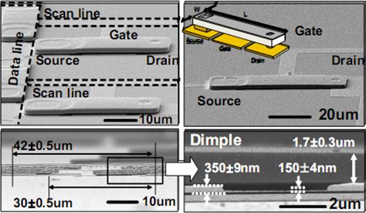
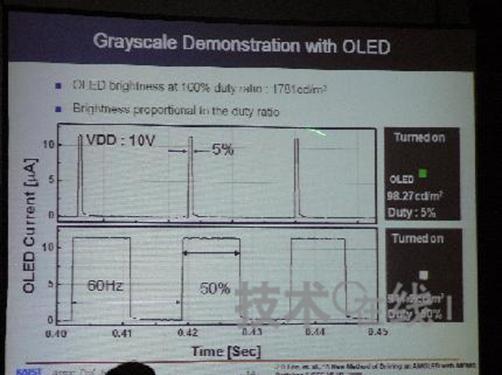
如图一与图二所示,KAIST试制了50 μm×10 μm的MEMS开关,电流可达15 mA;在hot switching模式底下(57 μA、100 Hz)可达1.3×10⁵个操作周期,相当于22分钟左右。如图三与图四所示,将该开关与有机EL组件连接并进行驱动,证实了数字灰阶显示的可能性,此次发表所获得的结果是:在电压VDD为10 V、脉冲频率为60 Hz的条件下,最大辉度为1781 cd/m2,duty cycle为50%时的辉度为914 cd/m2,duty cycle为5%的辉度为98.27 cd/m2。
中文新闻: http://big5.nikkeibp.co.jp/china/news/news/semi200805260112.html
|
|||||||||||||||||||||||
|
不睡枕头,小心落枕?
有此一说 不睡枕头容易落枕也容易造成颈部或脊椎的伤害?
KingNet
家庭医学科医师回答: 所谓的落枕,其实是颈部的筋膜炎,也就是因为颈部的肌肉不当使用或使用过度引起肌肉发炎以致于转动时造成疼痛。往往是因为枕头的柔软度、高度等因素,造成颈部姿势不自然,经过一个晚上的不当施力,而造成筋膜炎。
本文由【KingNet 国家网络医院】提供
|
|||||||||||||||||||||||
|
版权所有 国立台湾大学电机信息学院光电工程学研究所 http://gipo.ntu.edu.tw/ 欢迎转载 但请注明出处 http://gipo.ntu.edu.tw/monthly.htm |
|||||||||||||||||||||||