 |
||||||||||||||||||
|
|
||||||||||||||||||
|
�����ˣ����������� �༭ίԱ������ܽ��� ���ࣺ������ �������ڣ�2008.07.07 |
||||||||||||||||||
|
��
ʱ�䣺2008��6��13������4��30��~6��30�� ���ߣ�Dr.
Jean-Pierre Monchalin
(Group
Leader, Optical Diagnostics of Materials, Modelling and Diagnostics,
Industrial Materials Institute, National Research Council of Canada,
Canada) Dr. Jean-Pierre Monchalin ��2008��6��13�գ���������ݰ�ٱ������ʣ����ڲ�����101�ݽ���������˵������Ϊ��Optical Coherence Tomography and Ultrasound Modulated Optical Imaging at the Industrial Materials Institute of the National Research Council of Canada����������ʦ��ѧ�������Ҳ����ݽ��������������
�� |
||||||||||||||||||
|
�� �����Ͼ���ѧ��Nanjing University�� ��ʿ������� 2008 ��
��2008 ��һ��̨���ѧ—�Ͼ���ѧ��ѧ�ṹ�뼤�⼼����ʿ����̳�� ��ʱ�䣺2008��5��19����5��20�գ��ص㣺̨���ѧ�� �����������������ʿ��ѧ��¬��ة��������ѧ�����ӳ��� �������ܲμ���κ��Ͼ���ѧ����ϵ�Ľ�������������µ����ͼ������ۣ������Ͼ���ѧ����ʦ��ͬѧ������������ʮ��������̨�壬���ֻ����ڵ���ʮ����չ������εĽ�����ֳ����� ��ѧ�����ֻᡢʵ���Ҳιۺ��Ļ�֮�á��г����£� ��
�� �ڻ������������ֹ��縱������������С���Э��������λ��Ա��Ŭ���£���εĽ���������ϴ��̨���ͬѧ�Ƕ��ԣ�����һ������֪�Լ����ԡ�Ԣ���������ڿ�ѧ�������ó̡���β����ͬѧ�У���ɭ��(�ӳ�)���Լ��á�֣�нܡ��ֲ�͢�������ܡ�����ׯ�����������������ҡ�����������ͻȻ���£����μӽ�������������Ը�л���ڳﱸ�ڼ�Ϊ�������ֵľ������������ơ����Ҫ��л������Σ�������ݲ����������ϸ�ѧ���� �� û�Թ����⣬Ҳ��������·��ֻ��������·�������ԶҲ����֪�������ζ�������źܶ�ͬѧ���ڲμ�ѧ�����ֻ�����ϰ��Ϊ�������ˣ����ǣ��ﱸ���ֻ�Դ������ͬѧ����ȴ�Dz����й��ľ��顣��ε����ֻ���Ȼֻ�Ǹ���ʮ���˵�С�����ֻᣬ���ʻ��鶯�������˵Ĺ�ģ�����Ტ�ۣ������ɳﱸ��ε����ֻ��������������г̣������˽Ҫʹ��������Բ��˳������Ҫע��������DZ���һ��ʼԤ�����Ķ�ܶ࣬�����ﱸ���̶��Ҷ���ȷʵ���������ࡣ���⣬�������Dz���ͬѧ������������ذ�̨��������̨�����ɫ�渵�������ƽ��ֻ���������ѧУ���ص��Ҹе�ʮ�ֵغ��ա���͢������һ���ĵ���λ�ü�̨���ҵ���൱��Ϥ����ׯ���������̨�������ľ��㼰��ʳ����ָ�ƣ��нܸ���λ�ܳ��ĵ��Σ���·������Ϊ�ϴ��ͬѧ����̨������֣����Ҳ��ò�������Ȼ����ʵ����ε�ʵ���Ҳιۺ��Ļ�֮�ã�������ط����Ҳ���ȥ�����Ǻܾ�ûȥ�ģ����Ҫ��л�����г̵�ͬѧ������������ʶ��˵��г̡�������εĽ������Ҳ���Ҷ�����������һ��ε���ᡣ �� �ʹ�½��ѧ�������������еĻ���Ī�����������⡣���Ŵ��Ҳ���ܺ��棬��������Ļ��⣬���������Ӧ�ԡ������ϣ�����������ϴ��ͬѧ��̨�ηû�������ȥ��ȥ��½�������廪��ѧ�μ����ֻᣬ��½��ͬѧ��������̫�������ἰ����Ļ��⣻��Ȼ������Ҳ��������ȥ�ᡣ���ž�����������еġ��������顢����˫Ӯ���ɡ������ǽ������ⷽ�棬��������ر�С�ģ�����һ����С�ľͲ�ǹ�����Ū�ò�����ɢ���дΣ��Һ�ijλ�ϴ��ͬѧ������ʱ����������������������һ�γ����𣿡����ı���ͻȻ�Ե��е��㵣��ƺ���֪����λش���Ҳ�����������ʴ����ˣ�δ�����ػ��������̸��ʡ��������һ���뿪��½�𣿡�����Ц�Ÿ����ң���������һ���뿪��½������֮�⣬�ʹ�½��ͬѧ�ദ����������������ʲô�ر�֮�����ͺ�������ƽ����ͬѧ�ദ��������ұȽϺ���Ļ��⣬����Ŀǰ�����IJ��죬��½�DZߵ�ѧ����˶ʿ�����ꡢ��ʿ�����꣬���������˶ʿ����꣬��ʿ����˿������컯��������Ķ��������ڡ����⣬����˵����˶ʿ���ҵȥҵ�磬��һ��Ĺ�������н��Լ����ǧ��������ң�Ȼ������ʿ��ҵ����ѧУ����ʦ(�൱�����ǵ���������)��нˮ��������ǧ����ҡ��������ұȽϾ��ȵģ���̨�弸�������ҵ�˶ʿ��н�Ȳ�ʿ�ߵĹ����� �� ��ͺ����͢�����ϴ��ͬѧ�������ں����ǽ�����ͬʱ�������Լ�Ҳ�ڽ������ڲμ���εĽ����֮ǰ�������кܶ�ͬѧ��ʵ�DZ�������ʶ���Dz���ģ�������εĽ������Ҳ������һ��Ļ��ᡣ������������������ѧ�Ľ����������Ƶ����Ȼ���������ڵĽ����ȴ�Ե�����ѷ����ڼ����������ѧ������ͬʱ���Ƿ�Ҳ���Ծٰ�һЩ���ڵĽ��������������Ӫ�����ڸ����ʵ����ա� ��
�� �� |
||||||||||||||||||
|
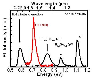
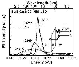
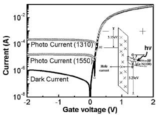
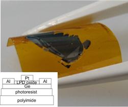
�� SiGe Based Optoelectronics T. -H. Cheng and C. W. Liu Graduate Institute of Photonics and Optoelectronics, National Taiwan University (e-mail) chee@cc.ee.ntu.edu.tw ̨���ѧ���������Ϊ���� It is a long sought goal to integrate ultra-large scale integrated (ULSI) circuits with the electro-optics to possibly overcome the speed limitation of electrical interconnects and to add extra functionalities on Si chip. LEDs and detectors are essential devices to achieve this goal. The most common material systems used for the light-emitting technology are III-V-based systems. However, due to the compatibility with Si electronics, the Si-based light emitters are the holy grails for the full integration of electrical and optical devices. Besides the 1.1��m infrared emission from Si band edge, the addition of Ge into Si can tune the optical characteristic to longer wavelength infrared emission from ~1.1��m to ~2.2��m wavelength (Fig. 1). The wavelengths of ~1.3��m, ~1.5��m, and ~2.2��m infrared have been achieved by Si0.8Ge0.2 Quantum well, Si0.45Ge0.55 quantum dot, Si/Si0.2Ge0.8 type-II heterojunction MIS LED, respectively. Moreover, due to the high carrier mobility, strong photon absorption, and possible integration with Si, the Ge based optoelectronic device also attracts great interest for scientific research and practical applications, recently. We develop successfully a Ge MIS tunneling diodes to serve both as a light emitter (~1.8��m) and a photodetector at a suitable bias. �� Figure 2 shows the EL spectra from an Al/SiO2/Ge MIS tunneling diode under continuous-wave operation at room temperature. The simulated line shapes from the electron-hole-plasma recombination model have a good agreement with the experimental data. The extracted band gaps using the electron hole plasma model are 40 meV lower than the Ge band gap obtained from Varshni��s equation from 65 to 345 K. This energy reduction is due to the longitudinal acoustic (LA) and longitudinal optic (LO) phonon replica in the radiative recombination, the band gap renormalization, and a significant amount of heat locally at the high injection current density. The inset of Fig. 2 depicts the schematic band diagram of the MIS tunneling diode for EL operation. At the positive gate voltage, an accumulation layer of majority electrons is formed at the Ge/SiO2 interface. The tunneling holes from the Al electrode recombine with electrons accumulated at the Ge/SiO2 interface and result in the radiative EL. Interface roughness, phonons, and the spread in k-space due to localized electrons can provide the extra momentum during the electron-hole-radiative recombination to emit the photons. �� When the MIS tunneling diode is biased at the inversion region, it can serve as a photodetector. The typical dark and photo currents of a bulk Ge (100) MIS photodetector under different wavelength exposures are shown in Fig. 3. The Ge MIS photodetector has a responsivity of 0.180 and 0.053 A/W at the wavelengths of 1310 and 1550 nm, respectively. The main reasons for the smaller responsivity in the MIS structure are the interface states at the insulator/semiconductor interface and the larger light reflectance of Al electrode. The inset of Fig. 3 shows the band diagram of the Ge MIS photodetector at inversion bias. The inversion bias can cause the deep depletion region to collect the photo-generated carriers. The minority carriers are generated in the deep depletion region, tunnel from the active absorption layer to the Al gate electrode via the trap-assisted tunneling of the LPD oxide, and form the photocurrent. �� Data communication between the Ge MIS LED and the Ge MIS photodetector is also demonstrated up to 15 Mbit/sec. The speed limitation is mainly due to the function generator in our system and can be enhanced with the high-speed modulator or detector. Other photodetectors such as GOG (Ge-on-Glass), GOI (Ge-on-Insulator), and GOP (Ge-on-Polyimide) are also developed to reach the goal of low cost, high speed, and extra functionality by wafer bonding and smart-cut technique. Figure 4 shows the photograph of flexible GOP structure. The thickness of the transferred Ge layer is about 1.6 ��m, and the surface roughness of the GOP structure is ~ 11 nm after the smart-cut process. Al with a ring area was evaporated on Ge. Since the Al ohmic contact has a large area (>0.1 cm2) and the barrier height between Al and Ge is small (0.1 eV), the effect of contact resistance is small. The low-temperature (50��) liquid phase deposited (LPD) oxide and Pt gate were used as the gate stack inside the Al ring. �� As time goes by, the solar cell plays a more and more important role to solve the energy crisis problem. In order to enhance the efficiency of solar cell, the simulation of optimized grid space, nano-texture structure, and external strain are added on the solar cell. The optical methods such as photoluminescence (PL) and electroluminescence (EL) are used to analysis the characteristics of solar cell. Minority carrier lifetime and diffusion length can be measured by temporal response of the electroluminescence and laser beam induced current (LBIC) to analysis the solar cell characteristics. �� ��
|
||||||||||||||||||
|
�� ������Ŀ����Һ������̬���Ǿ�̬�л��뵼��֮双�������Ӵ��������о� ������������ ָ�����ڣ�������
�� �� |
||||||||||||||||||
|
�� — �����ṩ��Ӱ����ʾ���Ƽ���ɫ�˲��������ģ�Ӱ����ʾ�Ƽ�֪ʶƽ̨ — — �������ֻ��ҽ��ڡ��¹��� — ��
2008 SID���ֻό��֮һ����������뵼��IGZO��In-Ga-Zn-O�����������ձ�ֻ�м��ܺͶ�����ҵ��ѧС���1������������ȫ������̨���ѧ���Ϻ�����ҵ���о������������Ϻ����̷���֮Ŀ����ȷΪ����ʵ�ִ���Ļ�л�EL���ӱ���Ĵ����TFT�װ������Ϻ�����SDI������ʵ��82��4K��2K TFTҺ������240Hz���������Ϻ����ǵ��ӣ�������IGZO�������ձ����������ϸҰ���ۿ��������ļ��������ۿ�����Ϊ�ƶ��ü�������ʾ���ϵ�Ӧ�ö������ؽ����о��Ϳ�����ȴ�����ձ������龰����Ȼ���˸е��� �����еĵ��¶�ᾧ�裨p-Si��TFT�ȹ�뵼����ȣ�������뵼��TFT���������ռ�����ɱ�Ҳ�dz������������л�EL����ڳɱ����������Ͻ�Һ�����������ˣ�����������뵼��TFT�����л�EL����Ϊ���ͳɱ���һ����Ҫ�ֶΡ����⣬������뵼��TFT�ĵ����ƶ��ȱȷǾ��裨a-Si��TFT��20���������ʾ����Ҳ�ϸߣ�������ʵ��ͼ��ĸ߷ֱ��ʣ���Ϊ�ߵ����ƶ��ȿ������������ʣ����Ϻ�����SDI�������˲���������뵼��IGZO����TFT�� 12.1���л�EL��壬��Ŀǰʹ����������뵼��TFT�Ƴ̼���������У��ò�Ʒ�ijߴ缰�ֱ��ʾ�Ϊ��� ��SID 2008���ֻ��ϸù�˾�����˼���ϸ�ڣ��ݽ���ţ�3.1�����˴ο������л�EL���Ļ���Ϊ1280��768���أ�WXGA�����ֱ���Ϊ123 ppi��ͼ1��������Ϊ300 cd/m2���Աȶ�Ϊ20000��1�����õײ�����ṹ�����TFT�װ�ȡ�á��л�EL���ϲ��õ��ǵͷ��Ӳ��ϣ�����ɫ������ϣ���ɫ����ɫ����ӫ����ϡ�TFT�Ĺ�������Ϊ7Ƭ�����ش�СΪ69 ��m��207 ��m�����ص�·��2��TFT��1�����������ɡ�բ��(gate)��Դ��(source)��©��(drain)�ĵ缫���ϲ���Mo��բ����ԵĤ����SiOx/SiNx����ʹ�������еĹ�����켼����IGZO TFT��Ǩ����Ϊ17.2 cm2/Vs�����رȴ���108������ֵб�ʣ�subthreshold gate swing��Ϊ0.28V/decade������SDIָ��������IGZO��TFT���������ڿ�������������ߴ粣���װ壬ʹ�ô˴ε�TFT������������������֧�ֵ�8���װ塣
�� �� ���ֶ��������������ţ� http://big5.nikkeibp.co.jp/china/news/news/flat200805230124.html �� �� �� |
||||||||||||||||||
|
�� ����������ഺ�����ã�
�д�һ˵�� ���ҽʦ�������⣬������������ڱ�˵ˢ����������ó����������������������������ͣ�ú�������֮�����Ƶ���ȫ���᳤�����ĵط�����ֻ�������������� ������Ҫ����ж��Լ��Ƿ�Ϊ���Է��ʣ�лл�� ��
KingNet
Ƥ����ҽʦ�ش���
����������ó���������������أ�����ģ� �� �����ɡ�KingNet ��������ҽԺ���ṩ �� |
||||||||||||||||||
|
��Ȩ���� ����̨���ѧ�����ϢѧԺ��繤��ѧ�о��� http://gipo.ntu.edu.tw/ ��ӭת�� ����ע������ http://gipo.ntu.edu.tw/monthly.htm |
||||||||||||||||||