發行人:楊志忠所長 編輯委員:蔡睿哲教授 主編:林筱文 發行日期:2006.12.01
![]() 「北北區影像顯示科技人才培育電子報」2006年第八期出刊囉∼
「北北區影像顯示科技人才培育電子報」2006年第八期出刊囉∼
「北北區影像顯示科技人才培育電子報」2006年第八期熱騰騰出爐囉!想知道影像顯示光電科技人才培育中心的最新消息與活動訊息嗎?歡迎踴躍點覽∼
![]() 本所12月演講公告:
本所12月演講公告:
| 日期 | 講者簡介 | 講題 | 地點 | 時間 |
|
12/06 |
John E. Bowers ECE Department University of California Santa Barbara |
Silicon Evanescent Photonic Integrated Circuits |
博理館 201 會議室 |
14:00-16:00 |
|
12/22 |
Prof. Chi H. Lee (李齊湘) University of Maryland, College Park, U.S.A. |
Polymer Photonics |
博理館 101 演講廳 |
16:30-18:30 |
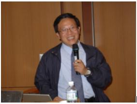
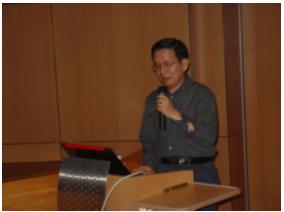
![]() 11月光電論壇演講花絮
11月光電論壇演講花絮
![]()
|
時間:11月3日下午4點30分
講者:張慶瑞主任(國立臺灣大學物理系系主任) 張慶瑞主任於95年11月3日蒞臨本所「光電論壇」演講;張主任專長為凝態物理理論及自旋相關電子在奈米結構的傳輸與應用。 |
|
|
|
時間:11月10日下午4點30分
講者:李鎮樟(DivX大使) "a personal perspective by an Angel" 李鎮樟為國際知名未來家與天使投資家。 李鎮樟曾在美國、臺灣、新加坡、香港等地的重要機構從事高科技開發、管理、策略規劃及投資等工作,曾幫助許多各國青年創業家建立世界級企業。今年開始以北京為基地,希望可以幫助更多國內外青年創業家,成功創立數位時代的標竿企業。 |
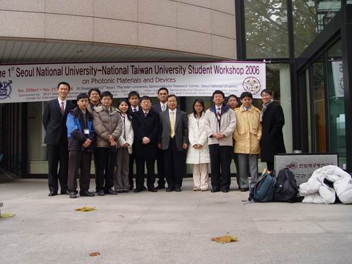
∼與韓國首爾大學博士生交流活動計畫∼
![]()
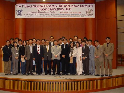
【第一屆臺灣大學—首爾大學光電子材料與元件研究生交流學術研討會】
(時間:95年11月19日至24日;地點:韓國首爾國立大學)
花絮整理:光電所博士班學生林皓武
第一屆台灣大學-首爾大學光電子材料與元件研究生交流學術研討會甫於2006年11月19日至11月24日於韓國首爾大學舉行。此次交流活動皆為雙方第一次舉辦此類的研討會,該研討會以雙方研究生為主,我們必須自己設計協商會議舉行方式,同時雙方各派代表主持會議,會議發表人也都是以研究生為主。
在這幾天的活動當中,參加此活動的韓國教授、學生們都非常熱情好客的招待我們。在交通、餐點以及會議規劃的安排上,都可以體會到他們細心週到的考量。在會議之外的參訪行程當中,他們也都相當大方的與我們交換各種心得,話題從彼此研究的主題開始,到語言、風俗、歷史、政治、宗教、經濟、食物、交通等各方面。在這些交流當中,我們了解到雖然彼此生長的環境不同,但其實彼此都有著類似的理想,價值觀也相去不遠。
此次會議的內容,大約可以分成六部分:(一)氮化物的成長、量測、分析,(二)奈米結構的成長、量測、分析,(三)發光元件,(四)有機發光二極體,(五)波導與非線性光學,(六)砷化銦鎵半導體。在三十分鐘的口頭報告中,內容包含介紹自己實驗室與個人研究題目。由於對雙方的研究生而言,大多數人是第一次發表如此長的英文口頭報告,除了發表自己學術研究上的成果外,還兼需簡介自己所屬實驗室的研究方向與貢獻,大家都以緊張、謹慎的態度準備並完成此次的演講。會議結束後緊接著是韓國大型實驗室的參訪,包括首爾大學內的 ISRC (Inter-university Semiconductor Research Center) 與位於首爾郊區的 KANC (Korea Advanced Nano Fab Center)。此次參訪讓我們體驗到韓國的研究環境以及研究精神。
雖然為了準備本次交流活動,大家的心情都是兢兢業業、緊張且興奮,但是結果卻是非常豐碩。在四天學術思考、文化風俗、語言溝通的衝擊下,大家都以滿載而歸的心情回國,但也踏出了我們研究生國際觀的第一步。
而這次能夠如此順利完成整個交流活動,需要感謝同行的三位教授:楊志忠所長、黃升龍副所長以及李允立教授,都十分辛苦的陪同、指導我們完成這次的交流活動,除此之外,陳正言隊長以及光電所辦公室的林筱文小姐在事前的準備上更是投入了許多的心力。而此次學校在經費上的贊助更是促成此行最重要的原因。雖然這次只是第一屆的交流活動,但我認為這次的活動對在台灣攻讀學位的研究生是相當有意義的,對我們的腦力、交流溝通的激盪更勝於參加一般國際研討會。希望這樣的活動能夠繼續的舉辦下去。我相信以後能有同學或學弟妹能夠繼續參加這樣的活動,一定也會有與我們有相同的感覺,在這樣的活動中,滿載而歸。
|
|
|
我方代表團與會教授、研究生與韓國主辦教授 Prof. Euijoon Yoon 合影 |
|
|
|
參與發表的雙方師長與學生於會議廳合影 |
|
|
劉致為教授 (C. W. Liu) Prof. Liu was born in Taipei, Taiwan, 1963. He received both the B.S. and M.S. degree in electrical engineering from National Taiwan University in 1985 and 1987, respectively. He received the Ph.D. degree in electrical engineering from Princeton University in 1994. |
|
|
He was with the department of Electrical Engineering, National Chung-Hsing University in 1994-95. He has joined the Department of Electrical Engineering, National Taiwan University as an associate Professor since 1996. In 2001, he became a full Professor. Prof. Liu also led a SiGe project in ERSO/ITRI through a special arrangement between NTU and ITRI as a research director with the rank of senior full researcher from 2001 to 2005. The research in Prof. Chee Wee Liu’s group is based on the SiGe:C and strained Si/high-K/metat gate, including (1) CMOS and Bipolar circuit design using (strained) Si CMOS and Si/SiGe:C HBTs; (2) device modeling and simulation on Strained Si/Ge FET, HBT, and optoelectronics devices; (3) CMOS optoelectronics with detector, emitter and waveguide; (4) material technologies such as SOI, GeOI, SSDOI, smart-cut, buckling quantum wells, nano-mechanics, and strained-SiGe:C; and (5) the rapid thermal processors for RTA, RTO, RTCVD, and wafer bonding. The strained Si/high-K/metal gate is intentionally to bypass the red brick wall on the ITRS roadmap, but the novel applications such as optoelectronics application are also focused. To lower the cost of strained Si technology, special local strain (process strain) technologies are being developed with calibrated process simulation.
The superior transport property of Ge can reach high performance target in the future CMOS technology. However, the cost and unstable Germanium oxide make it difficult to replace Si as industry mainstream. Recently, the structure of ultra thin Ge epitaxially directly grown on Si with compressive strain was proposed. The advantages of high mobility, low cost and compatibility with CMOS process are promising in the future technology.
The LED and photodetectors, and waveguides using available CMOS technology have been our focus since 1996. Now the LED efficiency, circuit integration, and speed are being improved with nanotechnolgy -enhancements such as Ge/SiC/SiGe quantumd dots, surface plasmom, high-K dielectrics, nanoroughness. Extremely small, highly efficient, and VLSI integratable devices are main purpose of this study. The high-K material research is focused on these novel applications as well as gate stacks.
New SOI, GeOI, SSDOI material using smart cut, wafer bonding, and nano-mechanics are developed for future device applications. New properties of buckled material and nano-strained material are found and will be incorporated to future device design.
Beside the well-equipped functions such as RTA, RTO, RTCVD, a new wafer bonding technique is developed, and other novel RTP functions will be installed. The uniformity and throughput is the current research focus.
Strained-Si technology has been used extensively as the mainstream Si industry. The method to enhance drive current and mobility of TFTs by external mechanical strain is proposed.
Integrated detector and TIA
The machine has the standard MESC interface, and it can be combined with cluster tool. Now it has functions of rapid thermal oxidation, rapid thermal annealing, chemical vapor deposition, and very high vacuum cleaning, and they can be performed in the same machine.
The Si CMOS has market size of ~200B USD in 2004. Without killer applications, it will be difficult to further increase its market size. The display has ~40B USD market size. Si can increase its market size by replacing the current technologies used in the display. The low cost and mature Si technologies can hopefully make LED display to outperform the TFTLCD in the display market. The indirect bandgap of Si and Ge makes the light emission from Si or Ge to be very inefficient (efficiency far less than a percent), and the bandgap of Si and Ge also limits the emission wavelength to infrared region (1.1 to 2 mm). We have tried very hard in the past decade to pump out the visible light from bulk Si by creating the hot electron/hot hole radiative recombination with the photon energy in the visible light range. Note that the switching speed of bulk Si MOS LED was around the order of m second, according to our previous results. This speed is sufficient for display applications. The quantum confinement of Si(Ge) nanocrystallite can have theoretical life time of ns. The III-V LED (light emitting diode) display is limited by cost and size and only has niche applications of the display market. The direct bandgap engineering and nanocrystallite Ge(Si) can potentially tune the emission wavelength into visible wavelength, and can increase the light emission efficiency to ~10%. The m sec speed of MOSLED is sufficient for display applications. Due to the emission location from the nanocrystllite embedded in the oxide of the MOS LED. The Si wafer is not necessary and a metal-anode/oxide with embedded nanocrystallite /metal-cathode (MIM LED) is proposed to inject carriers from Schottky barriers. This MIM LED can be potentially fabricated on glass substrate with the size comparable with TFTLCD. This technology will enable Si to share the display markets with TFTLCD technology.
v
劉教授對於同學們在學習方面有下列的建議: 1. 風簷展書讀,古道照顏色。 2. Team work is the most important.
|
||
固態發光及透明電子實驗室---黃建璋教授
黃建璋教授研究領域:
高效能發光二極體、奈米結構發光元件及材料、
有機及無機薄膜電機體製作及分析、可屈繞式透明電晶體及電路
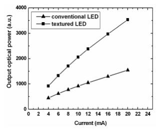
一、高效能發光二極體
我們以特殊之表面粗化方式,製作一高效能發光二極體,其發光效率比一般結構高180%。
|
|
二、矽材料發光:SiO2紅光加GaN藍光元件
我們發展出一種近白光的發光元件,將多孔隙的SiO2與藍綠光發光二極體結合,經過高溫退火後,矽的奈米晶體,將在多孔隙的SiO2膜中形成,利用電激發光(EL)量測,發現在低電壓時,仍是只有藍光出現,但當電壓增加,紅光波長強度逐漸增加,此乃是因為矽奈米晶體發光,將紅/藍/綠三種波長結合,形成近白光元件。
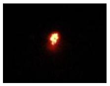 |
| 在高電壓時產生紅光 |
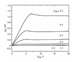
三、超高電流之ZnO TFT
新一代TFT半導體材料的候選者是以ZnO為主的氧化物,因為它具有透明度高,傳導率高的優勢。本研究是在改良ZnO-TFT的製程方式,達到最高效率的ZnO-TFT。我們以低溫製程的方式,全程不超過150度,做出高效能的TFT,目前的成果可以在VG=5V時,IDS=1mA,為目前世界最高紀錄。
 |
 |
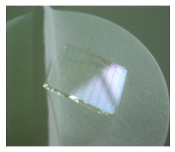
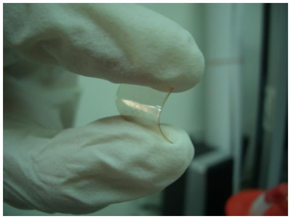
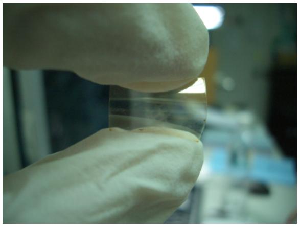
四、可撓式ZnO-based 透明TFT
軟性電子元件具有輕薄、可撓、耐衝擊 之特性,適用於行動電話、PDA或Notebook等可攜式產品。本研究是在塑膠基板上製作以氧化鋅為通道層之可撓式透明薄膜電晶體(Transparent Thin Film Transistors, TTFT),由於氧化鋅具有易於在低溫下利用濺渡法沉積於各種基板上的優點,因此可將TTFT製程溫度降低以符合塑膠基板本身的溫度限制。
|
|
|
|
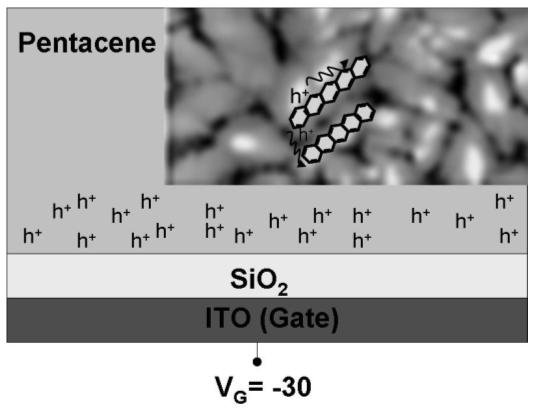
五、有機電晶體交流訊號分析及模型建立
我們與工研院合作,對pentacene有機電晶體做交流訊號分析及模型建立,目前對於C-V profile 已發展出一套定性的模型,此模型與一般crystalline 電晶體在C-V 上有特性上的差別。
 |
魚肝油+紅酒=消小腹?
![]()
有此一說:
日前在電視節目上報導,在睡前空腹吃兩顆魚肝油(要有 OMEGA 3 的成份),配上50∼100㏄紅酒,可以消除小腹。依據電視上醫生的說法是:可以促進新陳代謝率,加速脂肪的分解。
請問:(1) 是否此法可行?
(2) 成人一天魚肝油的攝取量要多少才適當呢?男女有差別嗎?
(3) 魚肝油中含的脂溶性維生素A、D、K,攝取過量是否會造成身體負擔?無法自行由體內排出?
醫師回答:
(1)睡前吃魚油加兩杯紅酒能消小腹,當然是道聽塗說。含有 OMEGA 3 魚油的魚肝油屬於健康食品,曾經有些
研究顯示可以升高好的膽固醇。但說能消小腹就太誇張了,因為如何確定吃下去的魚油只作用在小腹?至於紅
酒更是沒道理,曾經有些研究顯示紅酒可以預防心臟血管疾病。但是酒的熱量也很高。以這種方法減重保證不
行。
(2)至於魚肝油一天的攝取量,本人的建議是,沒事不用吃魚肝油。有事吃魚肝油也不能治病所以不用吃。
(3)食用過量確實會造成脂溶性維生素A、D、E、K囤積的可能。
本文由【KingNet 國家網路醫院】提供
版權所有 國立台灣大學電機資訊學院光電工程學研究所 http://eoe.ntu.edu.tw/
歡迎轉載 但請註明出處 http://eoe.ntu.edu.tw/monthly.htm